 | –≠–ª–µ–∫—Ç—Ä–æ–Ω–Ω—ã–π –∫–æ–º–ø–æ–Ω–µ–Ω—Ç: ADC1403X | –°–∫–∞—á–∞—Ç—å:  PDF PDF  ZIP ZIP |

ADC1403X
0.18
µ
µ
m 10-BIT 80MSPS ADC
1
GENERAL DESCRIPTION
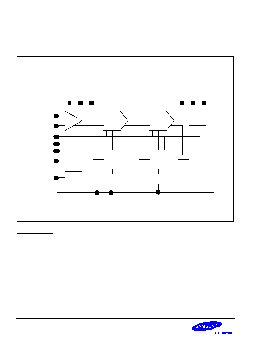
The adc1403x is a CMOS 10-bit low-voltage and high-speed A/D converter (ADC) for video and other applications. It
has a four-step pipelined architecture, which consists of sample & hold amplifier, multiplying D/A converters (DACs),
and subranging flash ADCs.
The maximum conversion rate of adc1403x is 80MSPS and supply voltage is 3.3V single.
FEATURES
-- Process : CMOS
-- Resolution : 10Bit
-- Maximum Conversion Rate : 80MSPS
-- Power Supply : 3.3V Single
-- Power Consumption : 363mW
-- Differential Linearity Error :
±
1.0 LSB (Typ)
-- Integral Linearity Error :
±
2.0 LSB (Typ)
-- Internal Sample-and-Hold
-- Internal Reference Generation
-- Operational Temperature Range : -40~85
∞
C
TYPICAL APPLICATIONS
-- Network Applications
≠ Ethernet, Wireless LAN
-- HDTV, High Resolution Digital TV
-- Portable equipments for low-power applications
0.18
µ
µ
m 10-BIT 80MSPS ADC
ADC1403X
2
FUNCTIONAL BLOCK DIAGRAM
MDAC1
SHA
Flash1
AINT
MDAC2
CML
Flash2
Flash3
MAINBS
CKGEN
DCLOGIC
AINC
REFTOP
REFBOT
REFMID
PD
CKIN
MINV
LINV
DO<9:0>
AVDD33A
AVSS33A
AVDD33D
AVSS33D
AVBB33D
AVBB33A
Ver 1.0 (Feb. 2002)
This datasheet is a preliminary version. No responsibility is assumed by SEC for its use nor for any infringements of
patents or other rights of third parties that may result from its use. The content of this datasheet is subject to change
without any notice.

ADC1403X
0.18
µ
µ
m 10-BIT 80MSPS ADC
3
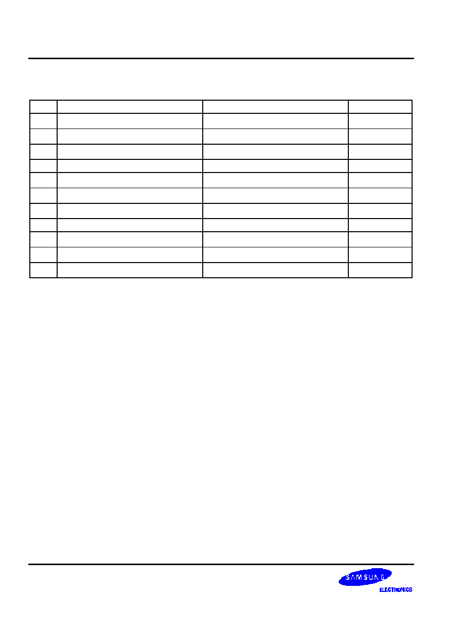
CORE PIN DESCRIPTION
Name
I/O Type
I/O Pad
Pin Description
AINT
AI
phiar50_abb
Analog Input (+1.9V ~ +1.4V)
AINC
AI
phiar50_abb
Analog Input (+1.4V ~ +1.9V)
REFMID
DI
phoa_abb
Ref Midpoint (Use Ext. BypassCap)
DO[9:0]
DO
phot16_abb
Digital Output
CKIN
DI
phicc_abb
External System Clock
REFTOP
AB
phia_abb
Reference Top Bias (+1.9V)
(Bypass Capacitor Required)
REFBOT
AB
phia_abb
Reference Bottom Bias (+1.4V)
(Bypass Capacitor Required)
MINV
DI
phicc_abb
Connect AVDD33D = Invert MSB
(Normally Connect AVSS33D)
LINV
DI
phicc_abb
Connect AVDD33D = Invert all LSBs
(Normally Connect AVSS33D)
AVDD33A
AP
vdd3t_abb
Analog Power (+3.3V)
AVSS33A
AG
vss3t_abb
Analog Ground (0.0V)
AVBB33A
AG
vbb3_abb
Analog Substrate Bias (0.0V)
AVDD33D
DP
vdd3t_abb
Digital Power (+3.3V)
AVSS33D
DG
vss3t_abb
Digital Ground (0.0V)
AVBB33D
DG
vbb3_abb
Digital Substrate Bias (0.0V)
I/O Type Abbr.
-- AI: Analog Input
-- DI: Digital Input
-- AO: Analog Output
-- DO: Digital Output
-- AB: Analog Bi-direction
-- DB: Digital Bi-direction
-- AP: Analog Power
-- AG: Analog Ground
-- DP: Digital Power
-- DG: Digital Ground

0.18
µ
µ
m 10-BIT 80MSPS ADC
ADC1403X
4
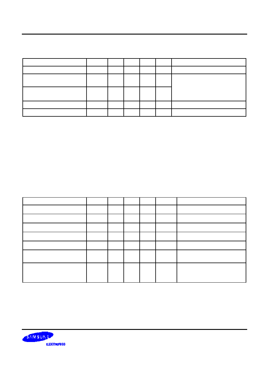
ABSOLUTE MAXIMUM RATINGS
Characteristic
Symbol
Value
Unit
Supply Voltage
AVDD33A
AVDD33D
-0.3 to 4.5
V
Analog Input Voltage
AIP/AINC
-0.3 to AVDD33A + 0.3
V
Digital Input Voltage
CK
-0.3 to AVDD33D + 0.3
V
Digital Output Voltage
V
OH
, V
OL
-0.3 to AVDD33D + 0.3
V
Storage Temperature Range
T
stg
-55 to 125
∞
C
NOTES:
1. Absolute maximum rating specifies the values beyond which the device may be damaged permanently. Exposure to
ABSOLUTE MAXIMUM RATING conditions for extended periods may affect reliability. Each condition value is applied
with the other values kept within the following operating conditions and function operation under any of these conditions
is not implied.
2.
A
ll
voltages
are
measured
with
respect
to
A
VSS33A/AVSS33D
unless
otherwise
specified.
3.
100pF
capacitor
is
discharged
through
a
1.5k
resistor
(Human
body
model).
RECOMMENDED OPERATING CONDITIONS
Characteristics
Symbol
Min
Typ
Max
Unit
Supply Voltage
AVDD33A - AVSS33A
AVDD33D - AVSS33D
3.0
3.3
3.6
V
Supply Voltage Difference
AVDD33A - AVDD33D
-0.1
0.0
0.1
V
Reference Input Voltage
REFTOP
REFBOT
≠
≠
1.9
1.4
≠
≠
V
Analog Input Voltage
AINT
AINC
1.4
≠
1.9
V
Clock High Time
Clock Low Time
T
pwh
T
pwl
≠
12.5
≠
ns
Digital Input 'L' Voltage
Digital Input 'H' Voltage
V
IL
V
IH
≠
3.0
≠
≠
0.3
≠
V
Operating Temperature
T
opr
-40
≠
85
∞
C
NOTES:
1. It
is
strongly
recommended
that
all
the
supply
pins
(AVDD33A,
A
VDD33D)
be
powered
from
the
same
source
to
avoid
power latch-up.
2. Reference Input Voltage REFTOP and REFBOT are generated internally and not adjustable.
ADC1403X
0.18
µ
µ
m 10-BIT 80MSPS ADC
5
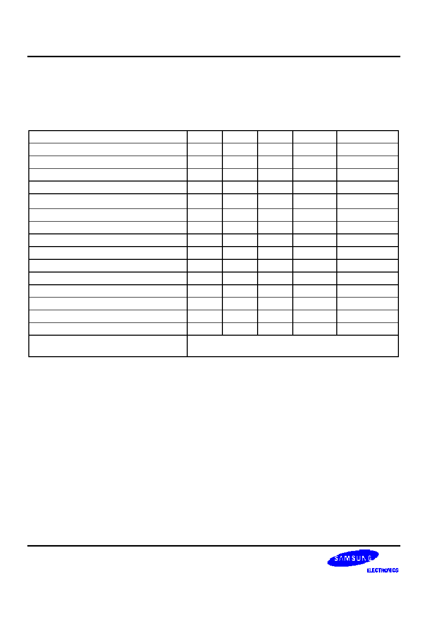
DC ELECTRICAL CHARACTERISTICS
Characteristics
Symbol
Min
Typ
Max
Unit
Test Conditions
Resolution
≠
≠
10
≠
Bits
≠
Differential Linearity Error
DLE
≠
±
0.5
±
1.0
LSB
AINT: 1.4V~ 1.9V(Ramp Input)
AINC: 1.9V~ 1.4V(Ramp Input)
Integral Linearity Error
ILE
≠
±
1.0
±
2.0
LSB
F
s
:
1MHz
20MHz
Bottom Offset Voltage Error
EOB
≠
≠
±
10
LSB
EOB = AI(0, 1) - 0
Top Offset Voltage Error
EOT
≠
≠
±
10
LSB
EOT = REFTOP - AI(1022, 1023)
NOTES:
1. Converter
Specifications
(unless
otherwise
specified)
AVDD33A=3.3V
AVDD33D=3.3V
AVSS33A=GND
AVSS33D=GND
SUBST=GND
REFTOP=1.9V
REFBOT=1.4V
MINV, LINV=Low
T
a
= 25
∞
C
2. AI(D1, D2) denotes the net voltage difference of AINT and AINC when the corresponding Digital Output code changes
from D1 to D2.
AC ELECTRICAL CHARACTERISTICS
Characteristics
Symbol
Min
Typ
Max
Unit
Test Conditions
Conversion Rate
F
s
≠
80
≠
MSPS
≠
Dynamic Supply Current
I
s
≠
110
120
mA
I
s
= I(AVDD33A) + I(AVDD33D)
Analog Input Range
V
in
≠
1.0
≠
V
PP
1.4V ~ 1.9V Differential Input
Analog Input Capacitance
C
in
≠
10
≠
pF
≠
Analog Input Bandwidth
F
in
≠
40
≠
MHz
≠
Digital Output Data Delay
T
d
≠
10
≠
ns
See
"DELAY TIMING DIAGRAM"
Signal to
Noise Distortion Ratio (SNDR)
SNDR1
SNDR2
SNDR3
≠
54
52
50
≠
dB
AIN : 1,20,40MHz respectively
(Sine Input)
F
s
: 80MHz
0.18
µ
µ
m 10-BIT 80MSPS ADC
ADC1403X
6
INPUT-OUTPUT MAPPING TABLE
Index
AINT (V)
AINC (V)
Digital Output
0
1.4V ~ 1.4V+1
◊
LSB
S
1.9V ~ 1.9V-1
◊
LSB
S
0000000000
1
1.4V+1
◊
LSB
S
~ 1.4V+2
◊
LSB
S
1.9V-1
◊
LSB
S
~ 1.9V-2
◊
LSB
S
0000000001
2
1.4V+2
◊
LSB
S
~ 1.4V+3
◊
LSB
S
1.9V-2
◊
LSB
S
~ 1.9V-3
◊
LSB
S
0000000010
∑
∑
∑
∑
∑
∑
∑
∑
∑
∑
∑
∑
511
1.4V+511
◊
LSB
S
~ 1.4V+512
◊
LSB
S
1.9V-511
◊
LSB
S
~ 1.9V-512
◊
LSB
S
0111111111
512
1.4V+512
◊
LSB
S
~ 1.4V+513
◊
LSB
S
1.9V+512
◊
LSB
S
~ 1.9V-513
◊
LSB
S
1000000000
513
1.4V+513
◊
LSB
S
~ 1.4V+514
◊
LSB
S
1.9V-513
◊
LSB
S
~ 1.9V-514
◊
LSB
S
1000000001
∑
∑
∑
∑
∑
∑
∑
∑
∑
∑
∑
∑
1021
1.4V+1021
◊
LSB
S
~ 1.4V+1022
◊
LSB
S
1.9V-1021
◊
LSB
S
~ 1.9V-1022
◊
LSB
S
1111111101
1022
1.4V+1022
◊
LSB
S
~ 1.4V+1023
◊
LSB
S
1.9V-1022
◊
LSB
S
~ 1.9V-1023
◊
LSB
S
1111111110
1023
1.4V+1023
◊
LSB
S
~ 1.9V
1.9V-1023
◊
LSB
S
~ 1.4V
1111111111
NOTES:
1. For Differential Input
.AINT = REFBOT ~ REFTOP
.AINC = REFTOP ~ REFBOT
.1
◊
LSB
D
= (REFTOP - REFBOT)/1024
and for Single Input
.AINT = (REFTOP + REFBOT)/2 - (REFTOP - REFBOT) ~ (REFTOP + REFBOT)/2 + (REFTOP - REFBOT)
.AINC = (REFTOP + REFBOT)/2
.1
◊
LSB
S
= 2
◊
(REFTOP - REFBOT)/1024
2. Using Differential Input Mode : AINT = 1.4 ~ 1.9, AINC = 1.9 ~ 1.4
1
◊
LSB
D
= (REFTOP - REFBOT)/1024 = 0.976562mV

ADC1403X
0.18
µ
µ
m 10-BIT 80MSPS ADC
7
TIMING DIAGRAM
DO[9:0]
DOUT1
DOUT2
Data Latency = 3.5 Clock
CKIN
D1
D2
AIN (= AINT-AINC)
0.18
µ
µ
m 10-BIT 80MSPS ADC
ADC1403X
8
FEEDBACK REQUEST
It should be quite helpful to our ADC core development if you specify your system requirements on ADC in the
following characteristic checking table and fill out the additional questions.
We appreciate your interest in our products. Thank you very much.
Characteristic
Min
Typ
Max
Unit
Remarks
Analog Power Supply Voltage
V
Digital Power Supply Voltage
V
Bit Resolution
Bit
Reference Input Voltage
V
Analog Input Voltage
V
PP
Operating Temperature
∞
C
Integral Non-linearity Error
LSB
Differential Non-linearity Error
LSB
Bottom Offset Voltage Error
mV
Top Offset Voltage Error
mV
Maximum Conversion Rate
MSPS
Dynamic Supply Current
mA
Power Dissipation
mW
Signal-to-noise Ratio
dB
Pipeline Delay
CLK
Digital Output Format
(Provide detailed description & timing diagram)
1. Between single input-output and differential input-output configurations, which one is suitable for your system
and why?
2. Please comment on the internal/external pin configurations you want our ADC to have, if you have any reason to
prefer some type of configuration.
3. Freely list those functions you want to be implemented in our ADC, if you have any.

ADC1403X
0.18
µ
µ
m 10-BIT 80MSPS ADC
9
HISTORY CARD
Version
Date
Modified Items
Comments
ver 1.0
02.02.05
Initial Release (preliminary version)
≠