 | –≠–ª–µ–∫—Ç—Ä–æ–Ω–Ω—ã–π –∫–æ–º–ø–æ–Ω–µ–Ω—Ç: al0402h | –°–∫–∞—á–∞—Ç—å:  PDF PDF  ZIP ZIP |

AL0402H
16-BIT 44.1KHZ SIGMA-DELTA STEREO DAC
1
GENERAL DESCRIPTION
This product is
Digital-To-Analog Converter for digital audio System (CDP). The product contains serial-to-
Parallel Converter and Compensation Filter , Digital Volume Attenuator by the MICOM Interface, De-Emphasis
Filter, FIR filter, Sinc Filter, digital sigma-delta modulator, analog postfilter, AIF (Anti-Image-Filter). The normal
input and output channels provide 95dB SNR (Signal to Noise Ratio) over in band (20kHz).
The product employs 1-bit 4th-order sigma-delta architecture with 16-bit resolution, over sampling of 64X. And
analog postfilter with low clock sensitivity and linear phase, filters the shaping-noise and outputs analog voltage
with high resolution. An on-chip reference voltage is included to allow single supply operations.
FEATURES
∑
16-bit
Digital-To-Analog Converter
∑
On-Chip Analog Postfilter
∑
Filtered Line-Level Outputs, Linear Phase
∑
On-Chip Voltage Reference
∑
95dB SNR
∑
Sampling Rate 44.1kHz
∑
Input Rate 1Fs or 2Fs by Normal Mode/Double Selection
∑
Zero Input Detection Mute
∑
On-Chip Compensation Filter
∑
Input Volume Attenuator by the MICOM Interface
∑
On-Chip De-Emphasis Filter
∑
On-Chip 4 times oversampling Digital Filter
∑
Single 5V Power Supply
∑
Low Clock Jitter Sensitivity

1-6BIT 44.1KHZ SIGMA-DELTA STEREO DAC
AL0402H
2
BLOCK DIAGRAM
SDATA
LRCK
BCK
MCK
AOUTL
VREF
IREF
AOUTR
S/P
Converter
&
Attenuator
Compensation
Filter
&
De-emphsis
&
FIR Filter
Sinc Filter
&
Sigma-Delta
Modulator
Analog
Postfilter
Anti-
Imaging
Filter
MICOM Interface
Timing Generation
Voltage
Reference
MLD
MCLK
MDATA
RSTB
DN
DEEM
PDL
MUTEL
TSEL
BIST_ON
IFS64
IADSL
IADSR
SERRORB
SDONE
DSLB
DSRB
Ver 1.1 (December 1998)
This datasheet is a preliminary version. No responsibility is assumed by SEC for its use nor for any infringements
of patents or other rights of third parties that may result from its use. The content of this datasheet is subject to
change without any notice.

AL0402H
16-BIT 44.1KHZ SIGMA-DELTA STEREO DAC
3
CORE PIN DESCRIPTION
Symbol
I/O Type
I/O Pad
Description
IADSL
DI
picc_bb
1-bit Input for Analog Postfilter of L-CH
(When TSEL = H, used)
IADSR
DI
picc_bb
1-bit Input for Analog Postfilter of R-CH
(When TSEL = H, used)
MDATA
DI
picc_bb
Micom Interface Command Data Input
SDATA
DI
picc_bb
Serial Digital Input
BCK
DI
picc_bb
Bit Clock Input
IFS64
DI
picc_bb
64X Sampling Clock Input for Analog Postfilter
(When TSEL = H, used)
LRCK
DI
picc_bb
Sample Rate Clock Input
MCK
DI
picc_bb
Master Clock Input
MCLK
DI
picc_bb
Micom Interface Clock Input
MLD
DI
picc_bb
Micom Interface Command load Input (When low, load)
BIST_ON
DI
picc_bb
Memory Bist Test Mode. "H" enabled
DEEM
DI
picc_bb
De-Emphasis On/Off. "H" is enabled. "L" is disabled.
DN
DI
picc_bb
Input Rate Select. High is Double (2Fs) Mode, Low is
Normal (1Fs) Mode.
MUTEL
DI
picc_bb
Analog Output Mute. "L" enabled
PDL
DI
picc_bb
Power Down. "L" enabled
RSTB
DI
picc_bb
Reset Input. "L" Enabled
TSEL
DI
picc_bb
Test pin for Analog Postfilter Input Selection
AOUTL
AO
poa_bb
Analog Output for L-CH
AOUTR
AO
poa_bb
Analog Output for R-CH
DSLB
DO
pot2_bb
L-CH 1bit Output for Digital sigma-delta Modulator.
DSRB
DO
pot2_bb
R-CH 1bit Output for Digital sigma-delta Modulator.
SDONE
DO
pot2_bb
Test Output pin for embedded memory BIST
(BIST_ON = "H") or Digital Block test (BIST_ON = "L")
SERRORB
DO
pot2_bb
Test Output Pin for Embedded memory BIST
(BIST_ON = "H") or Digital Block test (BIST_ON = "L")
IREF
AB
poa_bb
Test Pin for Analog Supply Current
VREF
AB
poa_bb
Reference Voltage Output for Bypass

1-6BIT 44.1KHZ SIGMA-DELTA STEREO DAC
AL0402H
4
CORE CONFIGURATION
al0402h
Used Power:
(VDDA VSSA VBB VDDD VSSD)
IADSL
IADSR
MDATA
SDATA
BCK
IFS64
LRCK
MCK
MCLK
MLD
BIST_ON
DEEM
DN
MUTEL
PDL
RSTB
TSEL
AOUTL
AOUTR
DSLB
DSRB
SDONE
SERRORB
IREF
VREF
ABSOLUTE MAXIMUM RATINGS
Characteristics
Symbol
Values
Unit
Supply Voltage
VDDD
VDDA
-0.3 to 7.0
V
Voltage on any Digital Voltage
Vin
VSSD-0.3 to VDDD+0.3
V
Storage Temperature Range
Tstg
-45 to 150
∞
C
NOTES:
1.
ABSOLUTE MAXIMUM RATING specifies the values beyond which the device may be damaged permanently. Exposure
to ABSOLUTE MAXIMUM RATING conditions for extended periods may affect reliability. Each condition value is applied
with the other values kept within the following operating conditions and function operation under any of these conditions
is not implied.
2. All voltages are measured with respect to Ground unless otherwise specified.
RECOMMENDED OPERATING CONDITIONS
Characteristics
Symbol
Min
Typ
Max
Unit
Supply Voltage
VDDD
VDDA
4.75
5.0
5.25
V
Operating Temp.
Topr
0
25
70
∞
C

AL0402H
16-BIT 44.1KHZ SIGMA-DELTA STEREO DAC
5
ELECTRICAL CHARACTERISTICS
(VDD = 5V, Temp = 25
∞
C, Fs = 44.1kHz, Signal Frequency = 20 to 20kHz)
Parameter
Min
Typ
Max
Units
Resolution
16
bits
SNR
<1>
90
95
dB
THD
<2>
0.007
0.004
%
SND
<3>
82
87
dB
Dynamic Range
<4>
85
90
dB
Reference Voltage Output
2.25
V
Frequency Response
±
0.1
±0.5
dB
Analog Output
Voltage Range
±
1.414
V
Load Impedance
5k
Digital Filter
Pass Band Ripple
±
0.0072
dB
Stop Band Attenuation
62.7
dB
Pass Band
0.45
Fs
Power Supply
Analog Current
25
mA
Digital Current
20
mA
Power Dissipation
225
mW
Power Down Current
1
mA
NOTES:
1.
1kHz 0dB Sinewave Input, EIAJ
2.
1kHz 0dB Sinewave Input
3.
1kHz 0dB Sinewave Input, (Not EIAJ)
Measured by Teledyne A585 System (using 30kHz LPF)
4.
1kHz -60dB Sinewve Input, and then measured data + 60dB

1-6BIT 44.1KHZ SIGMA-DELTA STEREO DAC
AL0402H
6
AC TIMING CHARACTERISTICS
(VDDD = 5V, VSSD = 0V,Temp = 25
∞
C)
Characteristics
Symbol
Min
Typ
Max
Unit
MCK Frequency
Fmck
-
16.9344
-
MHz
BCK Frequency (Normal/Double Mode)
Fbck
1.4112/
2.8224
-
MHz
MCK Rising and LRCK Edge Delay
Tmld
0
-
-
ns
MCK Rising and LRCK Edge Setup Time
Tmlst
10
-
-
ns
BCK Rising and LRCK Edge Delay
Tbld
0
-
-
ns
BCK Rising and LRCK Edge Setup Time
Tblst
10
-
-
ns
SDATA and BCK Rising Setup Time
Tsbst
10
-
-
ns
BCK Ring and SDATA Hold Time
Tbsht
10
-
-
ns
1/Fbck
MCK
BCK
0.5DVDD
1/Fmck
LRCK
Tmld
Tmlst
MCK
SDATA
LRCK
Tbld
Tblst
Tsbst
Tbsht
BCK
0.5DVDD
0.5 DVDD
0.5 DVDD
0.5 DVDD
0.5 DVDD
0.5 DVDD
Figure 1. Timing Diagram

AL0402H
16-BIT 44.1KHZ SIGMA-DELTA STEREO DAC
7
TIMING DIAGRAM (FS = 44.1KHZ)
Clock Input and Serial Input Data Inform
If DN(Double Mode/Normal Mode) pin is Low state, that is Normal Mode. And BCK, LRCK is following,
MCK = 384*Fs = 16.9344MHz
BCK = 32*Fs = 1.4112MHz
LRCK = 1*Fs = 44.1kHz
If DN pin is High state, that is Double mode. And BCK, LRCK is following,
MCK = 384*Fs = 16.9344MHz
BCK = 64*Fs = 2.8224MHz
LRCK = 2*Fs = 88.2kHz
SDATA is MSB first at falling edge triggered of BCK
LRCK
BCK
SDATA
R-CH DATA
L-CH DATA
MSB
MSB-1
MSB-2
LSB+2 LSB+11
LSB
MSB
MSB-1 MSB-2
LSB+2
LSB+1
LSB

1-6BIT 44.1KHZ SIGMA-DELTA STEREO DAC
AL0402H
8
FUNCTIONAL DESCRIPTION
Figure 2 is the 1-bit 4th-order sigma-delta DAC block diagram. S/P Converter converts serial 16-bit input data to
parallel 16-bit data. Digital input data is attenuated by MICOM interface pin control. Compensation Filter
compensates gain droop in Passband by Sinc Filter and Sigma-Delta Modulator Signal Transfer Function. De-
emphasis Block de-emphasizes pre-emphasized input data to emphasize high frequency in audible band. FIR
Filter performs 4X interpolation. And it outputs 4Fs (DN = 'Low') rate data or 8Fs (DN = 'High') rate data by
variabled input data rate. It also removes the images of the input signal that are present at multiples of the input
sample frequency. And Sinc filter makes the constant 64Fs rate data by 16 times 8 times upsampling FIR Filter
output data according to DN (Double/Normal Mode) Pin Selection. This operation introduces a sinc function
response on the resulting frequency spectrum, which greatly attenuates the energy of images at the multifules of
4Fs (or 8Fs).
Digital sigma-delta modulator of bit-stream type has the IFL (Inverse-Follower-Leader) topology, and it performs
a noise-shaping function. The modulator shapes the quantization noise by suppressing its in-band component
and pushes the noise energy of outside the band-of-interest without deteriorating the audio input signal. The 64
times oversampled 1-bit PDM output from the modulator the drives an analog postfilter.
The analog postfilter comprises SC-postfilter, anti-imaging filter. The SC-postfilter removes the quantization
noise shaped to out-of-band by digital sigma-delta modulator. This Analog filter has the good clock jitter
characteristic and very linear characteristic. And following the CTF (continuous time filter) removes the sampling
images and makes the high resolution analog output.
SDATA
AOUTL/
AOUTR
4Fs/8Fs
16-bit
1Fs/2Fs
16-bit
64Fs
1-bit
S/P
Converter
&
Attenuator
Compensation
Filter
&
De-emphasis
FIR & Filter
Sinc Filter
&
Modulator
SC-
Postfilter
CTF
(AIF)
Figure 2. 1 Bit Sigma-Delta DAC Block Diagram
MICOM INTERFACE
This product can do the function of digital attenuation whenever it receives thd MDATA, MLD, MCLK signals form
the MICOM.
DIGITAL ATTENUATION
When the 14-bit serial data is applied to the MDATA, MCLK, MLD in the form of Figure 3, according to the data
digital attenuation is accomplished. The lower eight LSBs should be 5D (LSB First Format-Hex) and according to
the upper 6-bit (LSB First Format-Bin) the attenuation level can be adjusted. (see Table1)
When RSTB is low state the latch circuitry for setting the attenuation level becomes reset and the attenuation
level is 0dB. At this instance, because the digital filter circuit gets to stop operation the act of attenuation is
impossible. In addition, whenever MDATA is not carried, MCLK must be 'HIGH' state. In case of no attenuation
function needed, MDATA should be 'L', MCLK and MLD should be 'H'.

AL0402H
16-BIT 44.1KHZ SIGMA-DELTA STEREO DAC
9
CORE EVALUATION GUIDE
M2
M3
M4
M5
Don't
Care
MCK
MDATA
MLD
M1
M0
Over 350ns needed
Don't
Care
Figure 3. MICOM Interface Timing Chart

1-6BIT 44.1KHZ SIGMA-DELTA STEREO DAC
AL0402H
10
Table1. Digital Attenuation Level
MDATA
Attenuation
MDATA
Attenuation
MSB LSB
M5 M4 M3 M2 M1 M0
Level (dB)
MSB LSB
M5 M4 M3 M2 M1 M0
Level (dB)
5 D 0 0 0 0 0 0
5 D 0 0 0 0 0 1
5 D 0 0 0 0 1 0
5 D 0 0 0 0 1 1
0
-0.28
-0.42
-0.56
5 D 1 0 0 0 0 0
5 D 1 0 0 0 0 1
5 D 1 0 0 0 1 0
5 D 1 0 0 0 1 1
-6.30
-6.58
-6.88
-7.18
5 D 0 0 0 1 0 0
5 D 0 0 0 1 0 1
5 D 0 0 0 1 1 0
5 D 0 0 0 1 1 1
-0.71
-0.86
-1.01
-1.16
5 D 1 0 0 1 0 0
5 D 1 0 0 1 0 1
5 D 1 0 0 1 1 0
5 D 1 0 0 1 1 1
-7.50
-7.82
-8.16
-8.52
5 D 0 0 1 0 0 0
5 D 0 0 1 0 0 1
5 D 0 0 1 0 1 0
5 D 0 0 1 0 1 1
-1.32
-1.48
-1.64
-1.80
5 D 1 0 1 0 0 0
5 D 1 0 1 0 0 1
5 D 1 0 1 0 1 0
5 D 1 0 1 0 1 1
-8.89
-9.28
-9.68
-10.10
5 D 0 0 1 1 0 0
5 D 0 0 1 1 0 1
5 D 0 0 1 1 1 0
5 D 0 0 1 1 1 1
-1.97
-2.14
-2.32
-2.50
5 D 1 0 1 1 0 0
5 D 1 0 1 1 0 1
5 D 1 0 1 1 1 0
5 D 1 0 1 1 1 1
-10.55
-11.02
-11.51
-12.04
5 D 0 1 0 0 0 0
5 D 0 1 0 0 0 1
5 D 0 1 0 0 1 0
5 D 0 1 0 0 1 1
-2.68
-2.87
-3.06
-3.25
5 D 1 1 0 0 0 0
5 D 1 1 0 0 0 1
5 D 1 1 0 0 1 0
5 D 1 1 0 0 1 1
-12.60
-13.20
-13.84
-14.54
5 D 0 1 0 1 0 0
5 D 0 1 0 1 0 1
5 D 0 1 0 1 1 0
5 D 0 1 0 1 1 1
-3.45
-3.66
-3.87
-4.08
5 D 1 1 0 1 0 0
5 D 1 1 0 1 0 1
5 D 1 1 0 1 1 0
5 D 1 1 0 1 1 1
-15.30
-16.12
-17.04
-18.06
5 D 0 1 1 0 0 0
5 D 0 1 1 0 0 1
5 D 0 1 1 0 1 0
5 D 0 1 1 0 1 1
-4.30
-4.53
-4.76
-5.00
5 D 1 1 1 0 0 0
5 D 1 1 1 0 0 1
5 D 1 1 1 0 1 0
5 D 1 1 1 0 1 1
-19.22
-20.56
-22.14
-24.08
5 D 0 1 1 1 0 0
5 D 0 1 1 1 0 1
5 D 0 1 1 1 1 0
5 D 0 1 1 1 1 1
-5.24
-5.49
-5.75
-6.02
5 D 1 1 1 1 0 0
5 D 1 1 1 1 0 1
5 D 1 1 1 1 1 0
5 D 1 1 1 1 1 1
-26.58
-30.10
-36.12
-

AL0402H
16-BIT 44.1KHZ SIGMA-DELTA STEREO DAC
11
SDATA
LRCK
BCK
MCK
AOUTL
VREF
AOUTR
DEEM
DN
RSTB
PDL
Audio Processor
(DSP)
al0402h
BIST_ON
TSEL
IFS64
IADSL
IADSR
MUX_Control
Digital Control Pins
Added Test Pins
IREF
0.1uF
10uF
1uF
External Application
MCLK
MDATA
MLD
Micom I/F Pins
for Digital Volume
control
SDATA
LRCK
BCK
MCK
VSSD
VSSA, VBB
0.1uF
10uF
VDDA
0.1uF
1uF
VDDD
If you don't want the internal test
mode, make the test control pins
disable state.('L')
If you don't want the internal test mode,
you don't need to make these pins and
leave these nodes foalting.
MUTEL
SERROR
SDONE
DSLB
DSRB
VSSD
VDDD
VDDA
VSSA
VBB
2 to 1
mux
(4x)
Digital Serial Input
and Clock Input
pins
VBB, VSSA Ground Pin should
be connected to analog ground.
Go to
Speaker
Driving
Opamp
100k
100k
1uF
∑
If you will test only analog core (al0402h), just add the 4 pins to supply digital inputs (LRCK, BCK, SDATA,
MUX_control)
∑
Digital serial input and clock input pins refer to timing diagram.
∑
Digital Control Pins inform refer to PIN Description.
∑
Analog powers (VDDA, VSSA, VBB) and digital powers (VDDD, VSSD) should be separated.
∑
VBB pin should be connected to analog ground.
∑
For Internal block test pins, if you don't need this mode, you make these pins to disable state ('L') and output
pins floating.
∑
This analog Core modeling (by Verilog) is provided.

1-6BIT 44.1KHZ SIGMA-DELTA STEREO DAC
AL0402H
12
APPLICATION GUIDE
∑
Locate bypass capacitors (0.1uF, 1uF, 10uF in pins VDDA, VDDD, Vref) as close as to Analog Core
∑
Vref line makes short and thick
∑
Analog and digital ground plane must be separated, and just connected by ferrite bead in one path.
CORE LAYOUT GUIDE
∑
VDDA, VSSA is the analog power of this core, and recommend that you should make pad for only this power.
∑
VBB (Bulk Bias) should be connected to VSSA pad (not internal VSSA line), or you should make pad for VBB
and externally connect to VSSA in board.
∑
VREF is analog reference pin, all VREF pin should be respectively connected to PAD for VREF (do not
internally merge and then go to pad for VREF)
∑
VSSA is analog ground pin, all VSSA pins should be respectively connected to PAD for VSSA.
∑
VDDA is analog supply pin, all VDDA pins should be respectively connected to PAD for VDDA.
∑
AOUTL and AOUTR which are analog output pins, should be connected to pad by way of thick and short.
AL0402H
16-BIT 44.1KHZ SIGMA-DELTA STEREO DAC
13
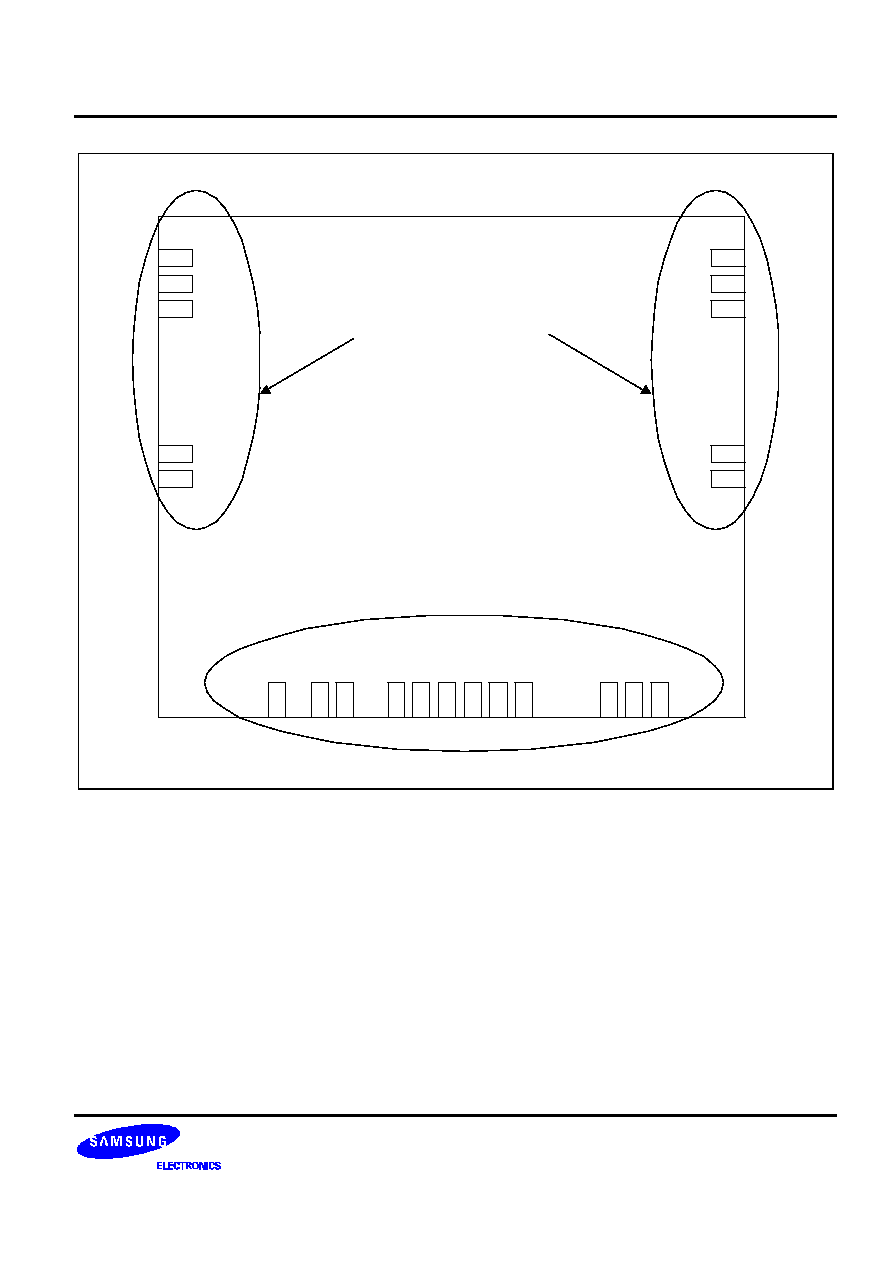
VDDD
VSSD
VDDD
VSSD
VDDD
VBB
VBB
All nodes go to pad repectively
Left and right nodes are same port, so
you must use only one-side of each
node.
VBB
VBB
VREF
VSSA
VREF
VDDA
VSSA
VSSA
VDDA
VSSA
VDDA
VSSA
VREF
VDDA
VDDD

1-6BIT 44.1KHZ SIGMA-DELTA STEREO DAC
AL0402H
14
FEEDBACK REQUEST
SIGMA-DELTA
DAC
SPECIFICATION
We appreciate your interest in our products. If you have further questions, please specify in the attached form.
Thank you very much.
Parameter
Min
Typ
Max
Unit
Remarks
supply voltage
V
Max master clock frequency
Hz
Operating temperature
∞C
Sampling Frequency
Hz
Dynamic range
dB
Total harmonic distortion
dB
Signal-to-noise ratio
dB
Input format resolution
(Serial/Parallel interface)
Bit
Channel
Mono
Stereo
Power dissipation
mW
Full scale output voltage range
Vpp
group delay
sec
Phase linearity deviation for passband
region
-
(Deg)
Peak-to-peak frequency response ripple for
passband region
dB
∑
Could
you
explain
external/internal
pin
configurations
as
required?
∑
Specially
requested
function
list
: