
The BL8531H_ADC is a CMOS 12bit analog-to-digital
converter (ADC).
It converts the analog input signal
into 12bit binary digital codes at a maximum
sampling rate of 10MHz.
The device is a monolithic ADC with an on-chip,
high-performance, sample-and-hold Amplifier (SHA)
and current referenc.
The structure allows both
differential and single-ended input.
This 12bit ADC has also 3 channel MUX, so 3
channel inputs are acceptable.
-
Resolution : 12bit
-
Maximum Conversion Rate : 10MHz
-
Power Supply : 5V
-
Power Consumption : 100mW (typical)
-
Reference Voltage : 3.5V, 1.5V (dual reference)
-
Input Range : 0.5V ~ 4.5V (4.0V
P-P
)
-
Differential Linearity Error : ±0.7 LSB
-
Integral Linearity Error : ±1.0 LSB
-
Signal to Noise & Distortion Ratio : 65dB
-
Total Harmonic Distortion : 74dB
- 3 Channel Inputs
-
Digital Output : CMOS Level
-
Operating Temperature Range : 0∫C
~ 70
∫C
GENERAL DESCRIPTION
FEATURES
FUNCTIONAL BLOCK DIAGRAM
CCD Imaging (Copiers, Scanners, Cameras)
Medical Instruments
Digital Communication Systems
TYPICAL APPLICATIONS
12BIT 10MSPS ADC
BL8531H_ADC
SAMSUNG ELECTRONICS Co. LTD
Ver 1.1 (Apr. 2002)
No responsibility is assumed by SEC for its use nor for any infringements of patents
or other rights of third parties that may result from its use. The content of this
datasheet is subject to change without any notice.
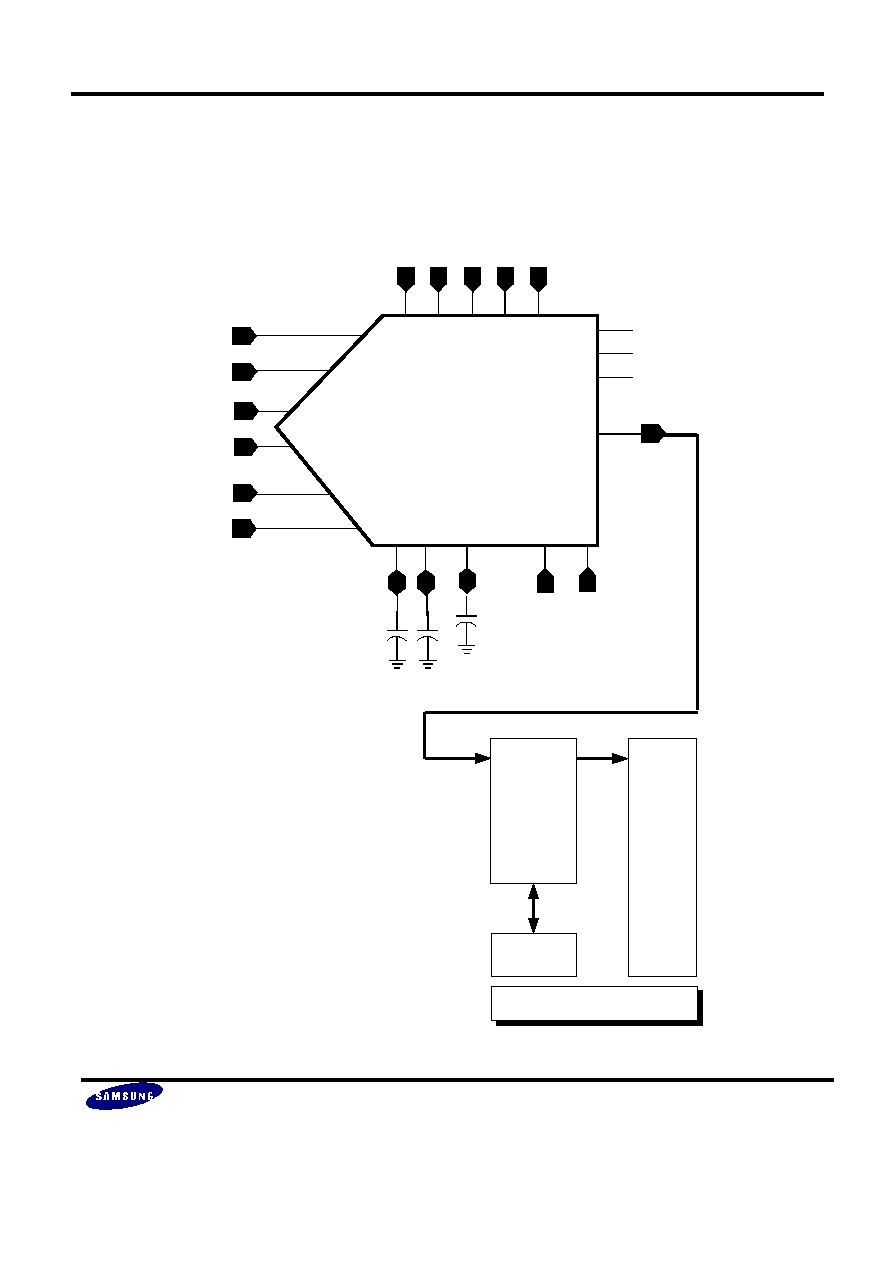
SHA
MDAC
2
MDAC
1
MDAC
3
FLASH
1
FLASH
2
FLASH
3
FLASH
4
DIGITAL
LOGIC
CLOCK
GEN.
3CH.
Analog
Inputs
Reference
Input
Clock
Digital
Output
Main
Bias
12
4
3
3
3

SEC ASIC
BL8531H_ADC
12BIT 10MSPS ADC
MIXED
CORE PIN DESCRIPTION
NAME
I/O TYPE I/O PAD
PIN DESCRIPTION
REFTOP
AO
poar10_bb Reference Top Force (3.5V)
REFBOT
AO
poar10_bb Reference Bottom Force (1.5V)
CML
AO
poar10_bb Internal Bias
VDDA
AP
vdda
Analog Power (5V)
VBB
AG
vbba
Analog Sub Bias
VSSA
AG
vssa
Analog Ground
R_INP
AI
piar10_bb
Analog Input (RED) +
(Input Range : 1.5V ~ 3.5V)
R_INN
AI
piar10_bb
Analog Input (RED) -
(Input Range : 1.5V ~ 3.5V)
G_INP
AI
piar10_b
Analog Input (GREEN) +
(Input Range : 1.5V ~ 3.5V)
G_INN
AI
piar10_bb
Analog Input (GREEN) -
(Input Range : 1.5V ~ 3.5V)
B_INP
AI
piar10_bb
Analog Input (BLUE) +
(Input Range : 1.5V ~ 3.5V)
B_INN
AI
piar10_bb
Analog Input (BLUE) -
(Input Range : 1.5V ~ 3.5V)
REDB
DI
picc_bb
RED Channel Select (0:select)
GREENB
DI
picc_bb
GREEN Channel Select (0:select)
BLUEB
DI
picc_bb
BLUE Channel Select (0:select)
STBY
DI
picc_bb
VDD=power saving (standby),
GND=normal
CKIN
DI
picc_bb
Sampling Clock Input
D[11:0]
DO
pot4_bb
Digital Output
VSSD
DG
vssd
Digital GND
VDDD
DP
vddd
Digital Power (5V)
I/O TYPE ABBR.
-AI : Analog Input
-DI : Digital Input
-AO : Analog Output
-DO : Analog Output
-AP : Analog Power
-AG : Analog Ground
-DP : Digital Power
-DG : Digital Ground
-AB : Analog Bidirection
-DB : Digital Bidirection
STBY CKIN
REFBOT CML
bl8531h_adc
R_INN
R_INP
REFTOP
vdda vssa
vbb vddd vssd
D[11:0]
[MSB:LSB]
B_INN
B_INP
G_INN
G_INP
¢∏ REDB
¢∏ GREENB
¢∏ BLUEB
2 / 11
SEC ASIC
BL8531H_ADC
12BIT 10MSPS ADC
MIXED
ABSOLUTE MAXIMUM RATINGS
Characteristics
Symbol
Value
Unit
Supply Voltage
VDD
6.0
V
Analog Input Voltage
R_INP/R_INN
G_INP/G_INN
B_INP/B_INN
VSS to VDD
V
Digital Input Voltage
CLK
VSS to VDD
V
Storage Temperature Range
Tstg
-45 to 150
∫C
Operating Temperature Range
Topr
0 to 70
∫C
NOTES
1. Absolute maximum rating specifies the values beyond which the device may be damaged permanently. Exposure to
ABSOLUTE MAXIMUM RATING conditions for extended periods may affect reliability. Each condition value is
applied with the other values kept within the following operating conditions and function operation under any of these
conditions is not implied.
2. All voltages are measured with respect to VSS unless otherwise specified.
3. 100pF capacitor is discharged through a 1.5k
resistor (Human body model)
RECOMMENDED OPERATING CONDITIONS
Characteristics
Symbol
Min
Typ
Max
Unit
Supply Voltage
VDDA1
VDDA2
VDDA3
4.75
5.0
5.25
V
Analog Input Voltage
R_INP/G_INP/B_INP
R_INN/G_INN/B_INN
0.5
-
2.5
4.5
V
Operating Temperature
Toper
0
-
70
∫C
NOTES
It is strongly recommended that all the supply pins (VDDA, VDDD) be powered from the same source to avoid power
latch-up.
3 / 11

SEC ASIC
BL8531H_ADC
12BIT 10MSPS ADC
MIXED
DC ELECTRICAL CHARACTERISTICS
Characteristics
Symbol
Min
Typ
Max
Unit
Test Condition
Differential
Nonlinearity
DNL
-
±
0.7
±
1
LSB
REFTOP=3.5V
REFBOT=1.5V
Integral
Nonlinearity
INL
-
±
1.0
-
LSB
Offset
Voltage
OFF
-
10
-
mV
(Converter Specifications : VDDA=VDDD=5V, VSSA=VSSD=0V,
Toper=25∞C, REFTOP=3.5V, REFBOT=1.5V unless otherwise specified)
AC ELECTRICAL CHARACTERISTICS
Characteristics
Symbol
Min
Typ
Max
Unit
Test Condition
Maximum
Conversion Rate
fc
-
10
MHz
AINR=R_INP-R_INN
AING=G_INP-G_INN
AING=B_INP-B_INN
Dynamic Supply
Current
IVDD
-
20
mA
fc=10MHz
(without system load)
Signal-to-Noise &
Distortion Ratio
SNDR
-
65
-
dB
AIN=1MHz,
Differential Input
Total Harmonic
Distortion
THD
-
74
-
dB
AIN=1MHz,
Differential Input
(Conversion Specifications : VDDA=VDDD=5V, VSSA=VSSD=0V,
Toper=25∞C, REFTOP=3.5V, REFBOT=1.5V unless otherwise specified)
4 / 11

SEC ASIC
BL8531H_ADC
12BIT 10MSPS ADC
MIXED
I/O CHART
Index
R_INP Input (V)
R_INN Input (v)
Digital Output
0
0.500 ~ 0.501
2.5
0000 0000 0000
RED Channel Input
Full Scale=4V
1LSB=0.977mV
REFTOP=3.5V
REFBOT=1.5V
1
0.501 ~ 1.502
2.5
0000 0000 0001
2
0.502 ~ 1.503
2.5
0000 0000 0010
°
°
°
8197
2.499 ~ 2.5000
2.5
0111 1111 1111
8192
2.500 ~ 2.501
2.5
1000 0000 0000
8193
2.501 ~ 2.502
2.5
1000 0000 0001
°
°
°
16381
4.497 ~ 4.498
2.5
1111 1111 1101
16382
4.498 ~ 4.499
2.5
1111 1111 1110
16383
4.499 ~ 4.500
2.5
1111 1111 1111
TIMING DIAGRAM
A1
A2
D1
D2
D3 D4
D5
A5
R_INP
G_INP
B_INP
CKIN
D[11:0]
Input Sampling Period
5 / 11

SEC ASIC
BL8531H_ADC
12BIT 10MSPS ADC
MIXED
FUNCTIONAL DESCRIPTION
1. The BL8531H_ADC is a CMOS four step pipelined Analog-to-Digital Converter. It contains 4-bit flash A/D
Converters, three 3bit flash A/D converters and three multiplying D/A Convertors. The N-bit flash ADC is
composed of 2
N
-1 latched comparators, and multiplying DAC is composed of 2*(2
N
+1) capacitors and two
fully-differential amplifiers.
2. The BL8531H_ADC operates as follows. During the first "L" cycle of external clock the analog input data is
sampled, and the input is held from the rising edge of the external clock, which is fed to the first 4-bit flash
ADC, and the first multiplying DAC. Multiplying DAC reconstructs a voltage corresponding to the first 4-bit
ADC's output, and finally amplifies a residue voltage by 2
4
. The second and third flash ADC, and MDAC are
worked as same manner. Finally amplified residue voltage at the third multiplying DAC is fed to the last 3-bit
flash ADC decides final 3-bit digital digital code.
3. BL8531H_ADC has the error correction scheme, which handles the output from mismatch in the first, second, third
and fourth flash ADC.
MAIN BLOCK DESCRIPTION
1. SHA
SHA (Sample-and-Hold Amplifier) is the circuit that samples the analog input signal and hold that value until next
sample-time. It is good as small as its different value between analog input signal and output signal. SHA amp
gain is higher than 70dB at 10MHz conversion rate, its settling-time must be shorten than 38ns with less than 1/2
LSB error voltage at 12bit resolution. This SHA is consist of fully differential op amp, switching tr. and sampling
capacitor. The sampling clock is non-overlapping clock (Q1, Q2) and sampling capacitor value is about 4pF. SHA
uses independent bias to protect interruption of any other circuit. SHA amp is designed that open-loop dc gain is
higher than 70dB, phase margin is higher than 60 degrees. Its input block is designed to be the rail-to-rail
architecture using complementary different pair.
2. FLASH
The 4-bit flash converters compare analog signal (SAH output) with reference voltage, and that results transfer to
MDAC and digital correction logic block. It is realized fully differential comparators of 15EA. Considering
self-offset, dynamic feed through error, it should distinguish 40mV at least. First, the comparators charge the
reference voltage at the sampling capacitors before transferred SHA output.That operation is performed on the phase
of Q2, and discharging on the phase of Q1. That is, the comparators compare relative different values dual input
voltage with dual reference voltage. Its output during Q1 operation is stored at the pre-latch block by Q1P.
3. MDAC
MDAC is the most important block at this ADC and it decides the characteristics. MDAC is consist of two stage
op amp, selection logic and capacitor array (c_array). c_array's compositions are the capacitors to charge the analog
input and and the reference voltage, switches to control the path. Selection logic controls the c_array internal
switches. If Q1 is high, selection's output are all low, the switches of tsw1 are off, the switches of tsw2 are all
on. Therefore the capacitors of c_array can charge analog input values held at SHA.
6 / 11
SEC ASIC
BL8531H_ADC
12BIT 10MSPS ADC
MIXED
CORE EVALUATION GUIDE
1. ADC function is evaluated by external check on the bidirectional pads connected to input nodes of HOST DSP
back-end circuit.
2. If User want the specific analog input range, the reference voltages may be forced.
D[110]
Digital Mux
Bidirectional
PAD
HOST
DSP
CORE
D[11:0]
D[110]
(ADC Function Test &
externally forced Digital Input)
bl8531h_adc
R_INN
R_INP
REFTOP
vdda vssa
vbb vddd vssd
D[11:0]
[MSB:LSB]
B_INN
B_INP
G_INN
G_INP
¢∏ REDB
¢∏ GREENB
¢∏ BLUEB
7 / 11

SEC ASIC
BL8531H_ADC
12BIT 10MSPS ADC
MIXED
USER GUIDE
1. Input Channel Select
- REDB, GREENB, BLUEB
- only 1 channel shoud be selected
- for example for RED channel select : REDB=0, GREENB=1, BLUEB=1
2. Input Range (for example : RED channel)
- If you want to using the single-ended input and RED channel is selected,
you should use he input range as below.
R_INP : 0.5V ~ 4.5V
R_INN : 2.5V
- If you want to using the differential input, you should use the input range as below.
R_INP : 1.5V ~ 3.5V,
R_INN : 1.5V ~ 3.5V.
AINR : R_INP
-
R_INN
- If you want to changing input range (AINR span), you can force reference voltages.
AIN span =
-
REF ~ +REF
REF = REFTOP
-
REFBOT
8 / 11

SEC ASIC
BL8531H_ADC
12BIT 10MSPS ADC
MIXED
PHANTOM CELL INFORMATION
- Pins of the core can be assigned externally (Package pins) or internally (internal ports) depending
on design methods.
The term "External" implies that the pins should be assigned externally like power pins.
The term "External/internal" implies that the applications of these pins depend on the user.
9 / 11
Pin Name
Pin Usage
Pin Layout Guide
VDDA
External
- Maintain the large width of lines as
far as the pads.
- place the port positions to minimize
the length of power lines.
- Do not merge the analog powers with
anoter power from other blocks.
- Use good power and ground source
on board.
VSSA
External
VBB
External
VDDD
External
VSSD
External
R_INP
External/Internal
- Do not overlap with digtal lines.
- Maintain the shotest path to pads.
R_INN
External/Internal
G_INP
External/Internal
G_INN
External/Internal
B_INP
External/Internal
B_INN
External/Internal
CKIN
External/Internal - Separate from all other analog signals
REFTOP
External/Internal - Maintain the larger width and the
shorter length as far as the pads.
- Separate from all other digital lines.
REFBOT
External/Internal
STBY
External/Internal
REDB
External/Internal
GREENB
External/Internal
BLUEB
External/Internal
DO[11]
External/Internal
- Separated from the analog clean
signals if possible.
- Do not exceed the length by 1,000um.
DO[10]
External/Internal
DO[9]
External/Internal
DO[8]
External/Internal
DO[7]
External/Internal
DO[6]
External/Internal
DO[5]
External/Internal
DO[4]
External/Internal
DO[3]
External/Internal
DO[2]
External/Internal
DO[1]
External/Internal
DO[0]
External/Internal
bl8531h_adc
12bit 10MSPS ADC
R
E
F
B
O
T
R
E
F
T
O
P
V
S
S
A
V
B
B
V
D
D
A
GREENB
R_INN
BUEB
REDB
R_INP
D
O
[
0
]
D
O
[
1
]
D
O
[
2
]
D
O
[
3
]
D
O
[
4
]
D
O
[
5
]
D
O
[
6
]
D
O
[
7
]
D
O
[
8
]
D
O
[
9
]
S
T
B
Y
V
D
D
D
V
B
B
V
S
S
D
C
K
I
N
G_INN
G_INP
B_INN
B_INP
D
O
[
1
0
]
D
O
[
1
1
]
V
S
S
A
V
B
B
V
D
D
A

SEC ASIC
BL8531H_ADC
12BIT 10MSPS ADC
MIXED
FEEDBACK REQUEST
It should be quite helpful to our ADC core development if you specify your system requirements on ADC in the
following characteristic checking table and fill out the additional questions.
We appreciate your interest in our products. Thank you very much.
Characteristic
Min
Typ
Max
Unit
Remarks
Analog Power Supply Voltage
V
Digital Power Supply Voltage
V
Bit Resolution
Bit
Reference Input Voltage
V
Analog Input Voltage
Vpp
Operating Temperature
∫C
Integral Non-linearity Error
LSB
Differential Non-linearity Error
LSB
Bottom Offset Voltage Error
mV
Top Offset Voltage Error
mV
Maximum Conversion Rate
MSPS
Dynamic Supply Current
mA
Power Dissipation
mW
Signal-to-noise Ratio
dB
Pipeline Delay
CLK
Digital Output Format
(Provide detailed description &
timing diagram)
1. Between single input-output and differential input-output configurations, which one is suitable for your system and
why?
2. Please comment on the internal/external pin configurations you want our ADC to have, if you have any reason to
prefer some type of configuration.
3. Freely list those functions you want to be implemented in our ADC, if you have any.
10 / 11

SEC ASIC
BL8531H_ADC
12BIT 10MSPS ADC
MIXED
HISTORY CARD
11 / 11
Version
Date
Modified Items
Comments
ver 1.0
99.12
Original version published (preliminary)
ver 1.1
02.4.17
Phantom information added and the format changed