 | ÐлекÑÑоннÑй компоненÑ: BW1223X | СкаÑаÑÑ:  PDF PDF  ZIP ZIP |
/home/web/htmldatasheet/RUSSIAN/html/samsung/188106

0.35
µ
µ
µ
µ
m 8-BIT 30MSPS ADC
BW1223X
1
GENERAL DESCRIPTION
The BW1223X is a CMOS 8-bit A/D converter for video applications. It is a two-step ping-pong A/D converter
which consists of reference resistor-matrix, 4-bit coarse and fine A/D converters.
The maximum conversion rate of BW1223X is 30MSPS and supply voltage is 3.3V single.
TYPICAL APPLICATIONS
-- Multi-media applications
-- Frame-grabber scanner
-- Camcorder
-- Digital video (TV/VCR)
-- Broadcasting and studio equipments.
-- Medical Electronics (ultra-sound and imaging)
-- High speed instruments (Digital scope, radar)
FEATURES
-- Process: CMOS
-- Resolution: 8Bit
-- Maximum Conversion Rate: 30MSPS
-- Power Supply: 3.3V Single
-- Power Consumption: 60mW
-- Differential Linearity Error: ¡¾0.2 LSB(Typ)
-- Integral Linearity Error: ¡¾0.3 LSB(Typ)
-- On-Chip Reference Bias Resistors
-- Reference Bias Adjustable Externally
BW1223X
0.35
µ
µ
µ
µ
m 8-BIT 30MSPS ADC
2
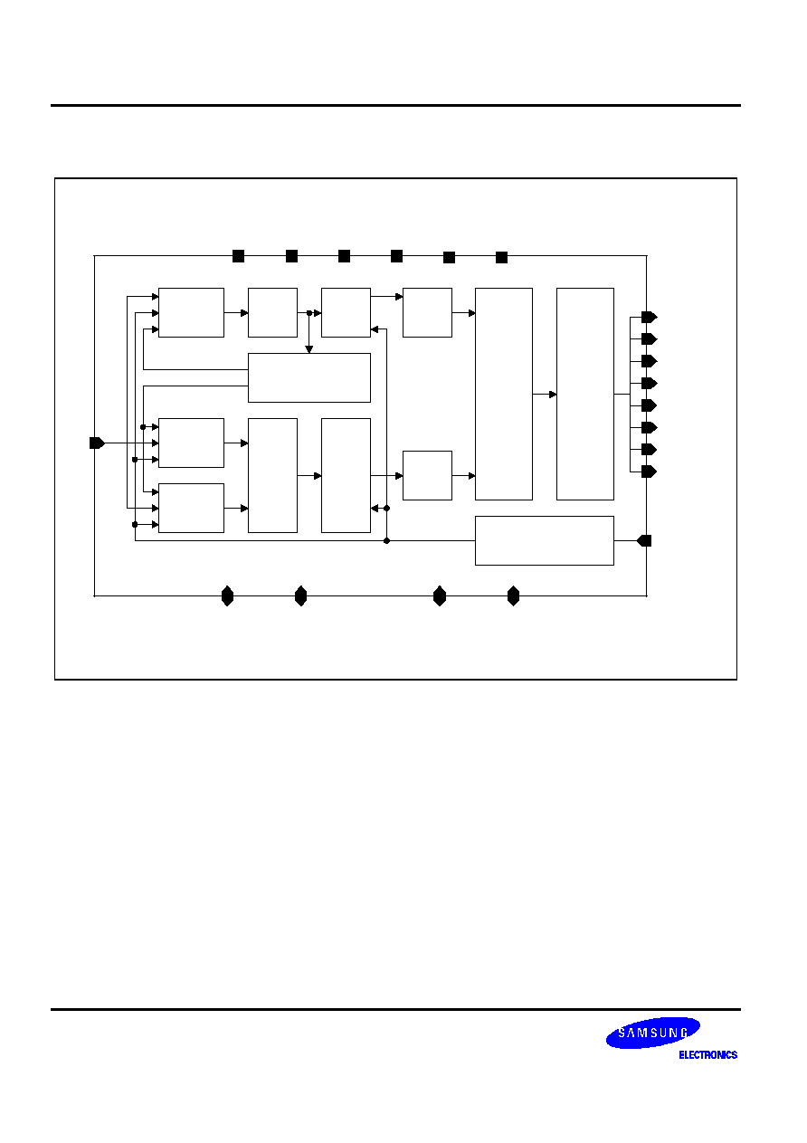
FUNCTIONAL BLOCK DIAGRAM
Coarse
Sampling
Amplifier
Latch
Analog
Mux
Latch
Reference
Matrix
Fine
Sampling
Amplifier
Fine
Sampling
Amplifier
Latch
FREE
COUT
Encoder
Encoder
Error
Correction
Circuit
Data
Latches
and
3-state
Output
Buffer
Timing Generator
DO[0] (LSB)
DO[1]
DO[2]
DO[3]
DO[4]
DO[5]
DO[6]
DO[7] (MSB)
VSSA
VDDA
VBBA
VDDD
VSSD
VBBD
VRB
VRT
VRBS
VRTS
AIN
FOUT
CLK
0.35
µ
µ
µ
µ
m 8-BIT 30MSPS ADC
BW1223X
3
CORE PIN DESCRIPTION
Name
I/O Type
I/O PAD
Pin Description
VRTS
AB
poa_bb
Internal Reference Top Bias
(Short to VRT for Self-Bias)
VRT
AB
poa_bb
2.6V External Reference Top Bias
VRBS
AB
poa_bb
Internal Reference Bottom Bias
(Short to VRB for Self-Bias)
VRB
AB
poa_bb
0.6V External Reference Bottom Bias
VDDA
AP
vdda
+3.3V Analog Power.
VBBA
AG
vbba
Analog Sub Bias.
VSSA
AG
vssa
Analog Ground.
AIN
AI
piar10_bb
Analog Input
Input Span : VRB ~ VRT
CLK
DI
picc_bb
Clock Input
DO[7:0]
DO
pot2_bb
Digital Output
VBBD
DG
vbba
Digital Sub Bias.
VSSD
DG
vssd
Digital Ground.
VDDD
DP
vddd
Digital Power.
I/O Type Abbr.
-- AI: Analog Input
-- DI: Digital Input
-- AO: Analog Output
-- DO: Digital Output
-- AB: Analog Bidirectional
-- DB: Digital Bidirectional
-- AP: Analog Power
-- DP: Digital Power
-- AG: Analog Ground
-- DG: Digital Ground
BW1223X
0.35
µ
µ
µ
µ
m 8-BIT 30MSPS ADC
4
CORE CONFIGURATION
BW1223X
CLK
AIN
DO[0] (LSB)
DO[1]
DO[2]
DO[3]
DO[4]
DO[5]
DO[6]
DO[7] (MSB)
VRT
S
VRB
VRT
VRB
S
VDD
A
VSS
A
VBB
A
VDD
D
VBB
D
VSS
D
0.35
µ
µ
µ
µ
m 8-BIT 30MSPS ADC
BW1223X
5
ABSOLUTE MAXIMUM RATINGS
Characteristics
Symbol
Value
Unit
Supply Voltage
VDD
-0.3 to 4.5
V
Analog Input Voltage
AIN
-0.3 to VDD+0.3
V
Digital Input Voltage
CLK
-0.3 to VDD+0.3
V
Digital Output Voltage
V
OH
, V
OL
-0.3 to VDD+0.3
V
Reference Voltage
VRT/VRB
-0.3 to VDD+0.3
V
Storage Temperature Range
T
stg
-45 to 125
°
C
NOTES:
1.
ABSOLUTE
MAXIMUM
RATING
specifies
the
values
beyond
which
the
device
may
be
damaged
permanently.
Exposure
to
ABSOLUTE
MAXIMUM
RATING
conditions
for
extended
periods
may
affect
reliability.
Each
condition
value
is
applied
with
the
other
values
kept
within
the
following
operating
conditions
and
function
operation
under
any
of
these
conditions
is
not
implied.
2.
All
voltages
are
measured
with
respect
to
VSS
unless
otherwise
specified.
3.
100pF
capacitor
is
discharged
through
a
1.5K
resistor
(Human
body
model)
RECOMMENDED OPERATING CONDITIONS
Characteristics
Symbol
Min
Typ
Max
Unit
Supply Voltage
VDDA - VSSA
VDDD - VSSD
3.15
3.3
3.45
V
Supply Voltage Difference
VDDA - VDDD
-0.1
0.0
0.1
V
Reference Input Voltage
VRT
VRB
2.6
0.6
V
Analog Input Voltage
AIN
VRB
VRT
V
Clock High Time
Clock Low Time
T
pwh
T
pwl
16.6
16.6
ns
Digital Input 'L' Voltage
Digital Input 'H' Voltage
V
IL
V
IH
3.0
0.3
V
Operating Temperature
T
opr
0
70
°
C
NOTE: It
is
strongly
recommended
that
all
the
supply
pins
(VDDA,
VDDD,
VDDP)
be
powered
from
the
same
source
to
avoid
power
latch-up.
BW1223X
0.35
µ
µ
µ
µ
m 8-BIT 30MSPS ADC
6
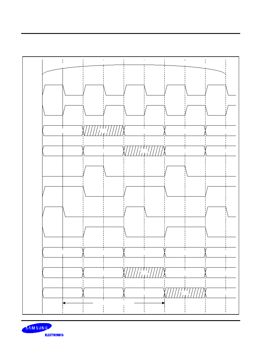
DC ELECTRICAL CHARACTERISTICS
Characteristics
Symbol
Min
Typ
Max
Unit
Conditions
Resolution
8
Bits
Reference Current
IREF
6.25
mA
VRT: 2.6V
VRB: 0.6V
Differential Linearity Error
DLE
±
0.3
±
0.5
LSB
AIN: 0.6 ~ 2.6V
(Ramp Input)
Integral Linearity Error
ILE
±
0.5
±
0.8
LSB
F
s
: 1MHz
20MHz
Bottom Offset Voltage Error
EOB
±
6.3
±
6.5
LSB
EOB = AIN(0,1) - VRB
Top Offset Voltage Error
EOT
±
5.4
±
5.6
LSB
EOT = VRT - AIN(254,255)
NOTES:
1.
Converter
Specifications
(unless
otherwise
specified)
VDDA=3.3V
VDDD=3.3V
VSSA=GND
VSSD=GND
Ta=25
°
C
2.
TBD:
To
Be
Determined
AC ELECTRICAL CHARACTERISTICS
Characteristics
Symbol
Min
Typ
Max
Unit
Conditions
Clock High Time
T
pwh
16.6
ns
Clock Low Time
T
pwl
16.6
ns
Conversion Rate
F
s
30
MSPS
Dynamic Supply Current
I
s
(IREF)
20
(6.25)
mA
I
s
= I(VDDA) + I(VDDD) + IREF
F
s
: 30MHz
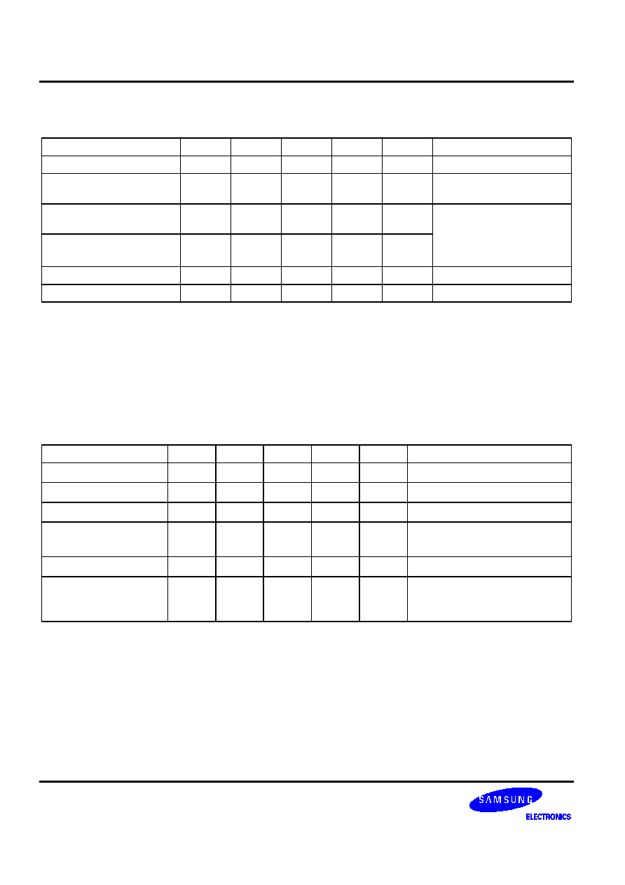
Digital Output Data Delay
t
d
18
30
ns
See "DELAY TIMING DIAGRAM"
Signal to
Noise Distortion
Ratio (SNDR)
SNR1
SNR2
SNR3
38
45
45
41
dB
AIN: 1, 2, 4MHz respectively
(Sine Input)
F
s
: 30MHz
0.35
µ
µ
µ
µ
m 8-BIT 30MSPS ADC
BW1223X
7
DELAY TIMING DIAGRAM
DO
DO (-2)
DO (-1)
DO (0)
DO (1)
2.5 CLK PIPELINE DELAY
td
CLK
AIN
A1
A1

BW1223X
0.35
µ
µ
µ
µ
m 8-BIT 30MSPS ADC
8
FUNCTIONAL DESCRIPTION
1. BW1223X is a two-step ping-pong A/D converter with subranging reference resistor matrix.
It consists of 4-bit coarse A/D converter and fine A/D converter of which the accuracy is 4.459 bits. The latching
comparators in coarse and fine A/D converters have offset cancellation features built in such as auto-zero and
averaging, and the number of comparators are 15 in the coarse converter and 42 in the fine one.
The sampling operation of fine A/D converter is performed, through 21 analog MUXs, in a ping-pong manner
between the two sampling amplifier banks each of which consists of 21 latching comparators.
2. The reference resistor matrix switch one of the 16 different sets of reference voltages, according to the states
of the coarse comparator digital outputs, to the fine sampling amplifier banks. This fact and the use of a CMOS
auto-zero comparator surely eliminate the extra pain for implementing high accuracy D/A converter of 8 bits or
more, and thus a low-power, high-performance and high speed A/D converter results.
3. The operation of BW1223X can be stated as follows. (refer to the 'TIMING DIAGRAM' that follows)
During the first cycle of external clock, the analog input 'AIN' is traced by each converter, and at the falling edge
of CLK the 'AIN' is sampled and held to be compared with the 16-level coarse reference voltages. The result of
comparison in coarse comparator, 'COUT', is latched and used to select a set of fine reference voltage 'FREF'
which, to be compared with the sampled analog input, is fed to the fine sampling amplifier banks. The result of
the comparison is reproduced by successive comparators with sufficiently large gain and then multiplexed to
the latching digital logic in a ping-pong manner. Latching logic in coarse and fine converters refine the results of
comparison to generate A/D converter output 'FOUT' and 'COUT', and from which the final digital output 'DO'
is generated.
The overall pipeline delay, measured from the sampling instance to the time that the 'DO' comes to be
available, is 2.5 clock cycles.
4. BW1223X implements the error correction scheme to correct the error which stems from the mismatch
between the offset of coarse A/D converter and that of the fine A/D converter. This scheme can handle coarse
comparator offset error up to 3 LSBs and helps reducing the differential linearity error consequently.
0.35
µ
µ
µ
µ
m 8-BIT 30MSPS ADC
BW1223X
9
TIMING DIAGRAM
Coarse
Sample
Coarse
Compare
FREF
COUT
Fine 1
Sample
Fine 1
Compare
Fine 2
Sample
Fine 2
Compare
MUX
OUT
FOUT
DO
AIN
A2
A3
A4
A5
A0
A1
A1
A2
A3
A4
A0
A1
A2
A3
FComp1
FComp2
FComp1
FComp2
FComp1
A0
A1
A2
A3
A0
A1
A2
2.5 Clock Pipeline Deley
BW1223X
0.35
µ
µ
µ
µ
m 8-BIT 30MSPS ADC
10
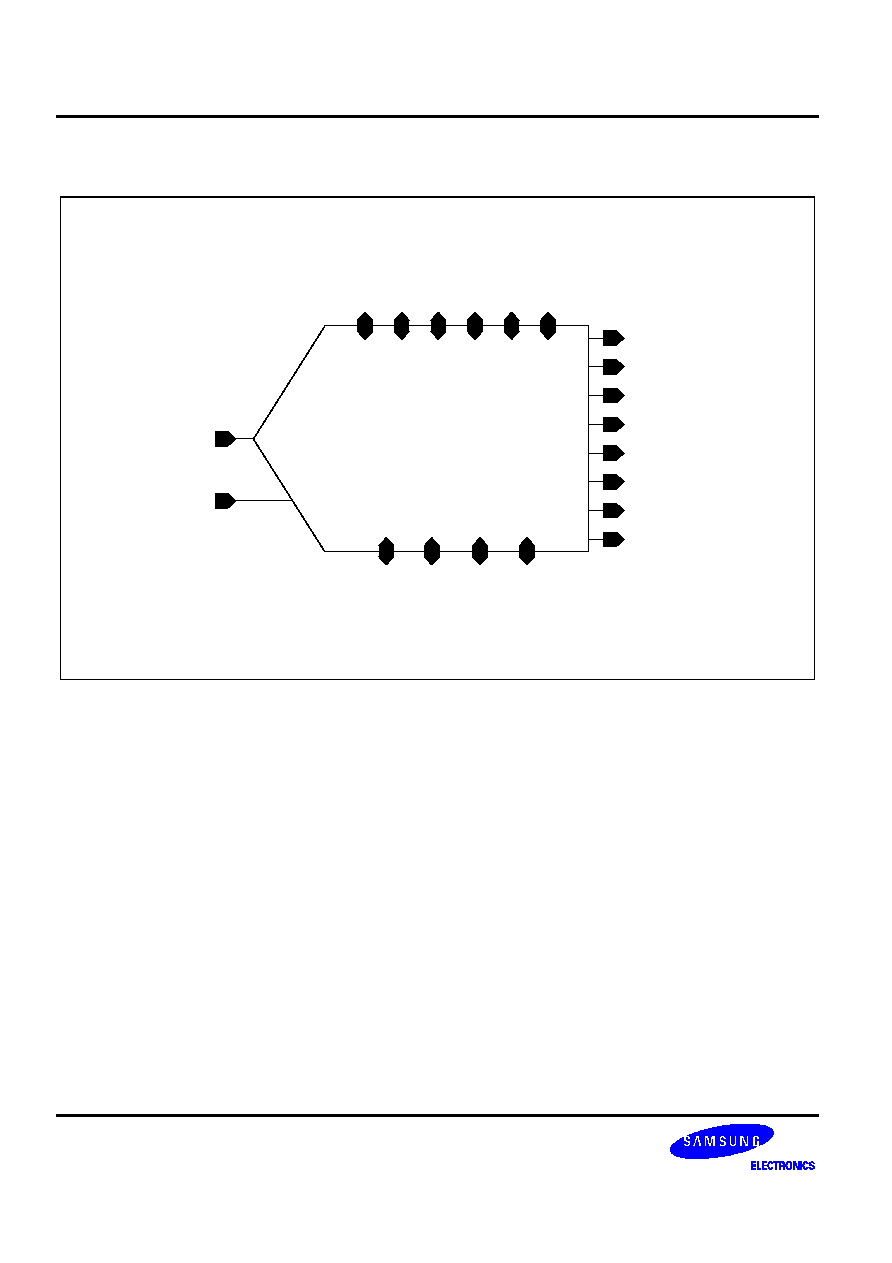
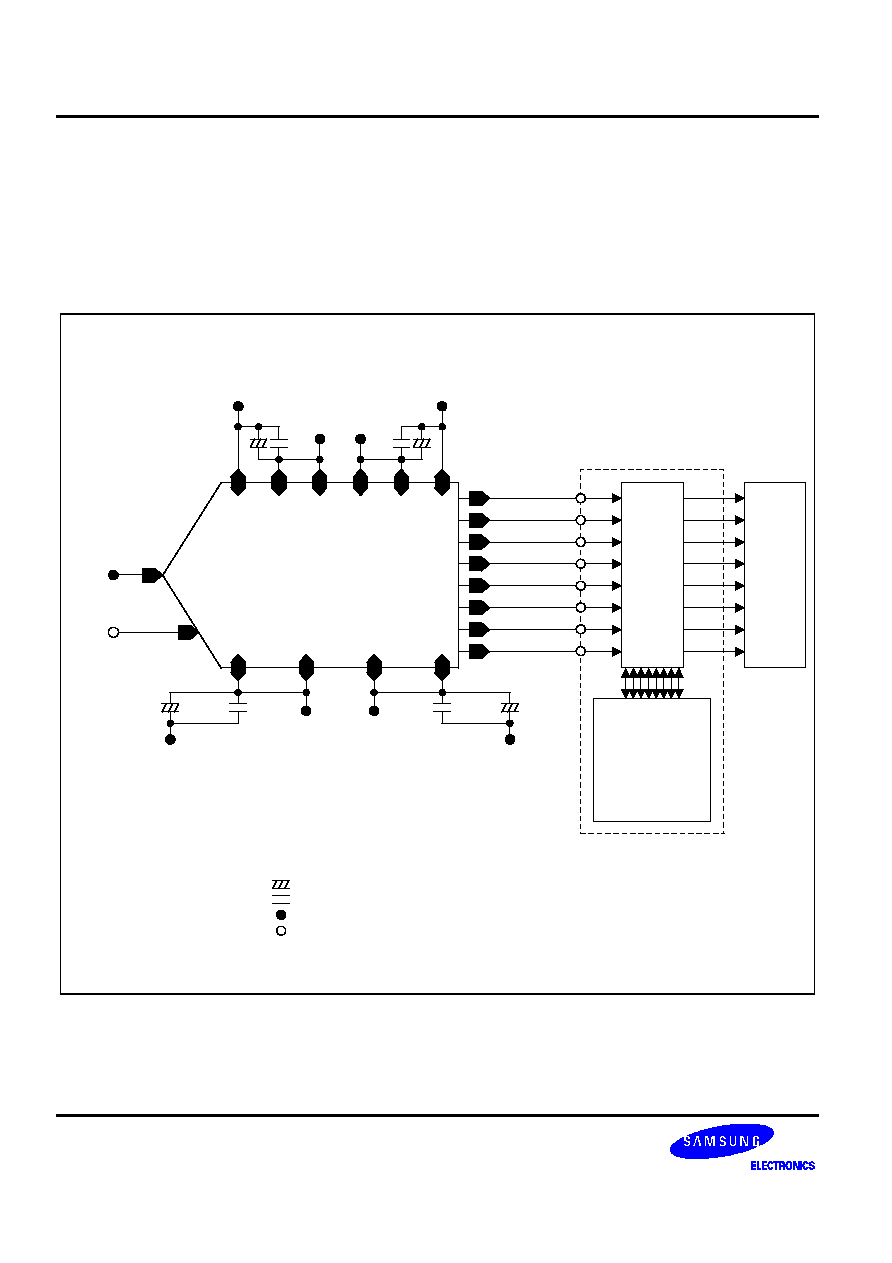
CORE EVALUATION GUIDE
1. ADC function is evaluated by external check on the bidirectional pads connected to input nodes of HOST DSP
back-end circuit.
2. The reference voltages may be biased externally through VRT and VRB pins, otherwise these voltages are
internally generated with VRT and VRB shorted to VRTS and VRBS respectively.
BW1223X
VDDA
MUX
HOST
DSP
CORE
Bidirectional Pad
ADC Function
Measuring
&
Digital Input
Forcing
AINC
CKIN
+3.3V
Analog Power
GND
+3.3V
Digital Power
GND
2.6V
Top
Reference
GND
0.6V
Bottom
Reference
GND
DO[0] (LSB)
DO[1]
DO[2]
DO[3]
DO[4]
DO[5]
DO[6]
DO[6] (MSB)
VSSA VBBA VBBD VSSD VDDD
VRTS
VRT
VRBS
VRB
NOTES:
1. : 10uF electrolytic capacitor unless otherwise specified
2. : 0.1uF ceramic capacitor unless otherwise specifed
3. : External pias.
4. : Internal pias.
0.35
µ
µ
µ
µ
m 8-BIT 30MSPS ADC
BW1223X
11
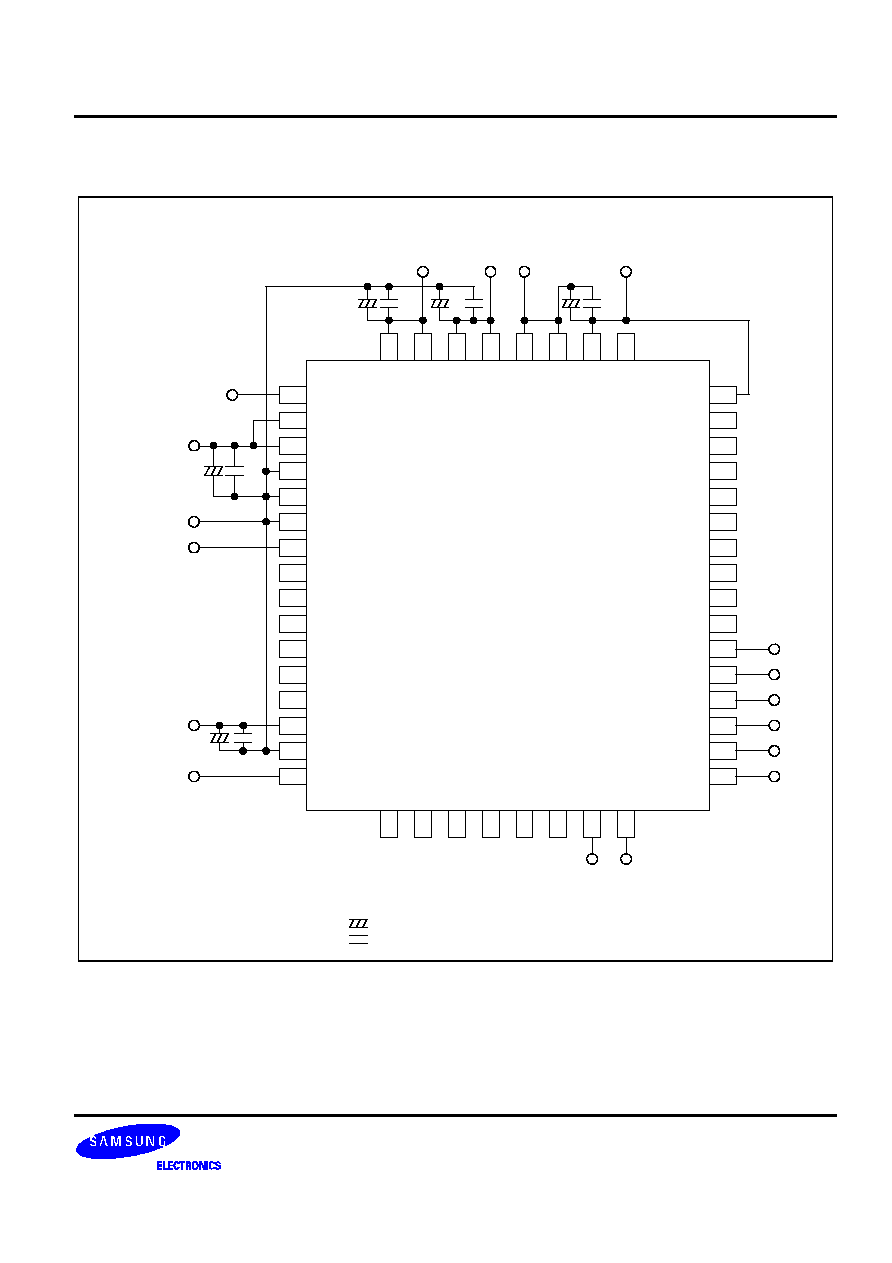
PACKAGE CONFIGURATION
BW1223X
VBBD
NC
NC
NC
NC
NC
NC
NC
NC
DO[5]
DO[4]
DO[3]
DO[2]
NC
DO[7]
DO[6]
44
43
42
41
40
39
38
37
36
35
34
33
32
31
30
29
NC
VDDA
VDDA
VBBA
VSSA
AINT
NC
NC
NC
NC
VDDP
VSSP
CLK
VSSA
NC
NC
5
6
7
8
9
10
11
12
13
14
15
16
17
18
19
20
3.3V
Analog Power
+0.6V
Reference
Bottom
+2.6V
Reference
Top
3.3V
Digital
Power
GND
NC
NC
NC
NC
NC
DO[
0
]
DO[
1
]
NC
27
26
28
25
24
23
22
21
VRB
S
VRT
S
VRT
VDD
D
VDD
D
VSS
D
VSS
D
VRB
46
47
45
48
1
2
3
4
Digital Output Bits 0 and 1
D
i
gi
tal O
u
tp
ut Bits
2 Throu
gh 7
NOTES:
1. : 10uF electrolytic capacitor unless otherwise specified
2. : 0.1uF ceramic capacitor unless otherwise specifed
GND
Analog Input
(Input Span = VRB-VRT)
3.3V
PAD Power
Clock Signal
NOTES:
1.
You
can
test
ADC
function
by
checking
external
bidirectional
pad
connected
to
internal
signal
path.
2.
ESD
(ElectroStatic
Discharge)
sensitive
device.
Although
the
digital
control
inputs
are
diode
protected,
permanent
damage
may
occur
on
devices
subjected
to
high
electrostatic
discharges.
It
is
recommended
that
unused
devices
be
stored
in
conductive
foam
or
shunts
to
avoid
performance
degradation
or
loss
of
functionality.
The
protective
foam
should
be
discharged
to
the
destination
socket
before
devices
are
inserted.
3.
NC
denotes
"No
Connection".
BW1223X
0.35
µ
µ
µ
µ
m 8-BIT 30MSPS ADC
12
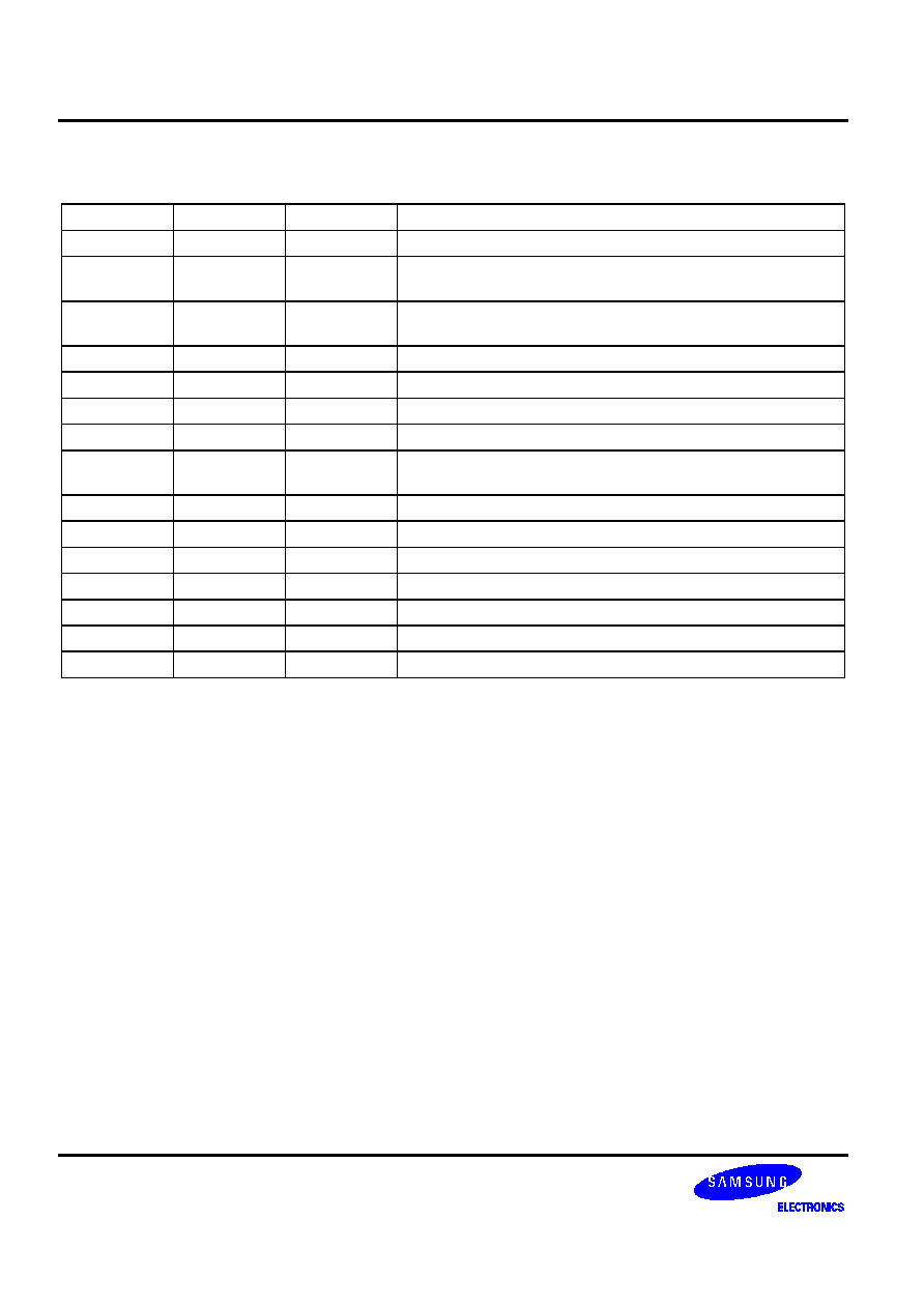
PACKAGE PIN DESCRIPTION
Name
Pin No.
I/O Type
Pin Description
VRT
1
AB
+2.6V External Reference Top Bias.
VRTS
2
AB
Internal Reference Top Bias.
(Short to VRTS for Self-Bias.)
VRBS
3
AB
Internal Reference Bottom Bias.
(Short to VRBS for Self-Bias.)
VRB
4
AB
+0.6V External Reference Bottom Bias.
VDDA
6, 7
AP
+3.3V Analog Power.
VBBA
8
AG
Analog Sub Bias.
VSSA
9, 10
AG
Analog Ground.
AIN
11
AI
Analog Input.
Input Span = VRT ~ VRB.
VDDP
18
DP
PAD Power
VSSP
19
DG
PAD Ground
CLK
20
DI
Clock Input.
DO[7:0]
34~27
DO
Digital Output.
VBBD
44
DG
Digital Sub Bias.
VSSD
45, 46
DG
Digital Ground.
VDDD
47, 48
DP
Digital Power.
I/O Type Abbr.
-- AI: Analog Input
-- DI: Digital Input
-- AO: Analog Output
-- DO: Digital Output
-- AB: Analog Bidirectional
-- DB: Digital Bidirectional
-- AP: Analog Power
-- DP: Digital Power
-- AG: Analog Ground
-- DG: Digital Ground