 | –≠–ª–µ–∫—Ç—Ä–æ–Ω–Ω—ã–π –∫–æ–º–ø–æ–Ω–µ–Ω—Ç: bw1244d | –°–∫–∞—á–∞—Ç—å:  PDF PDF  ZIP ZIP |

0.35
µ
µ
µ
µ
m 3.3 V 10-BIT 0.5MSPS DAC
BW1244D
1
GENERAL DESCRIPTION
The BW1244D is a CMOS 10Bit D/A converter for general application. This digital to analog converter has a R-2R
ladder structure. Its maximum conversion rate is 0.5MSPS
TYPICAL APPLICATIONS
-- Hard Disk Drive (HDD)
-- Battery Operated Instruments
-- Motor Control Systems
-- General Applications
FEATURES
-- Resolution : 10Bit
-- Differential Linearity Error : ± 1.0 LSB
-- Integral Linearity Error : ± 2.0 LSB
-- Maximum Conversion Rate : 0.5MSPS
-- Low Power Consumption : 9.9mW
-- Power Down Mode
-- Operation Temperature Range : 0∫C ~ 70∫C
-- Power Supply : 3.3V Single
BW1244D
0.35
µ
µ
µ
µ
m 3.3 V 10-BIT 0.5MSPS DAC
2
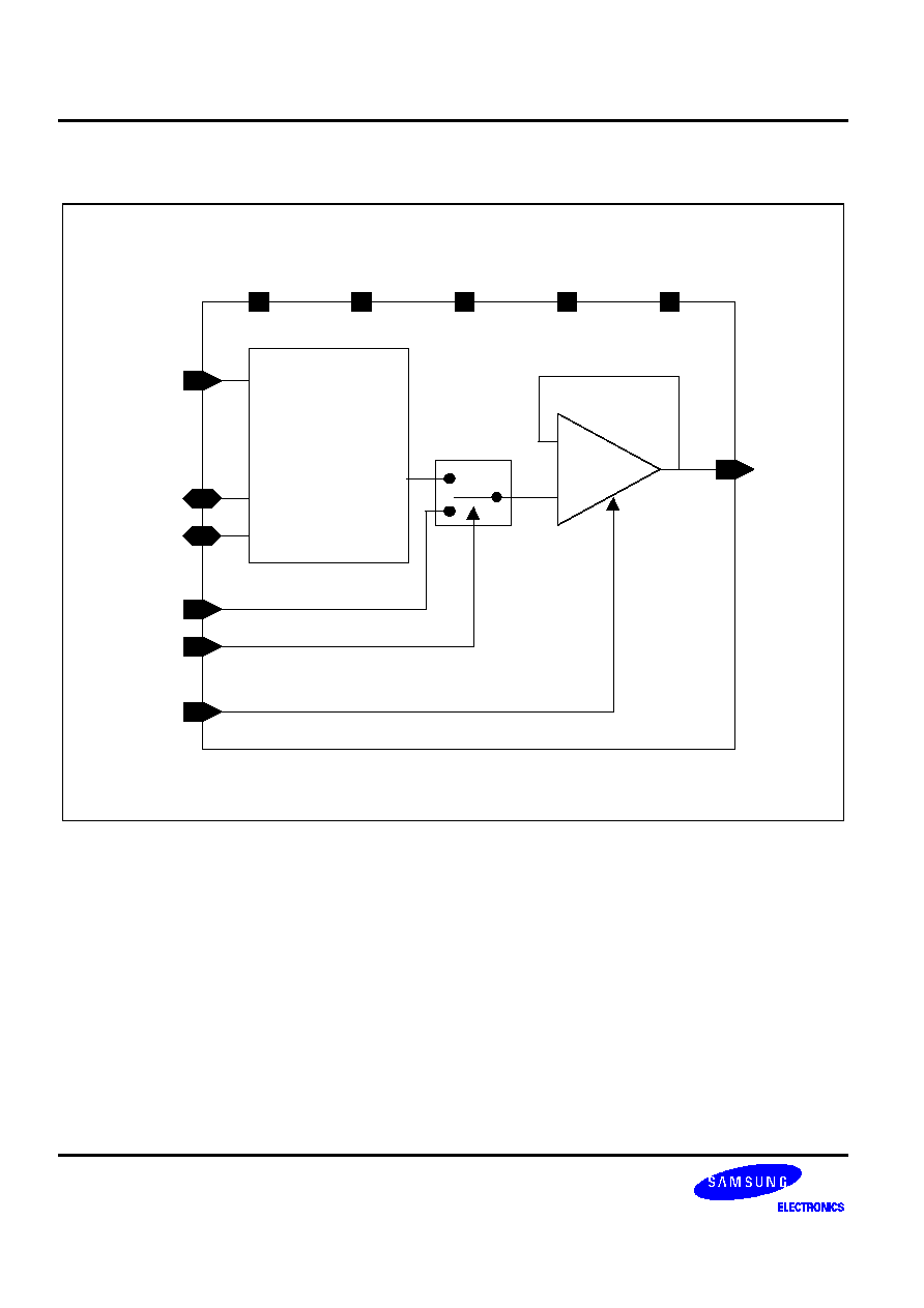
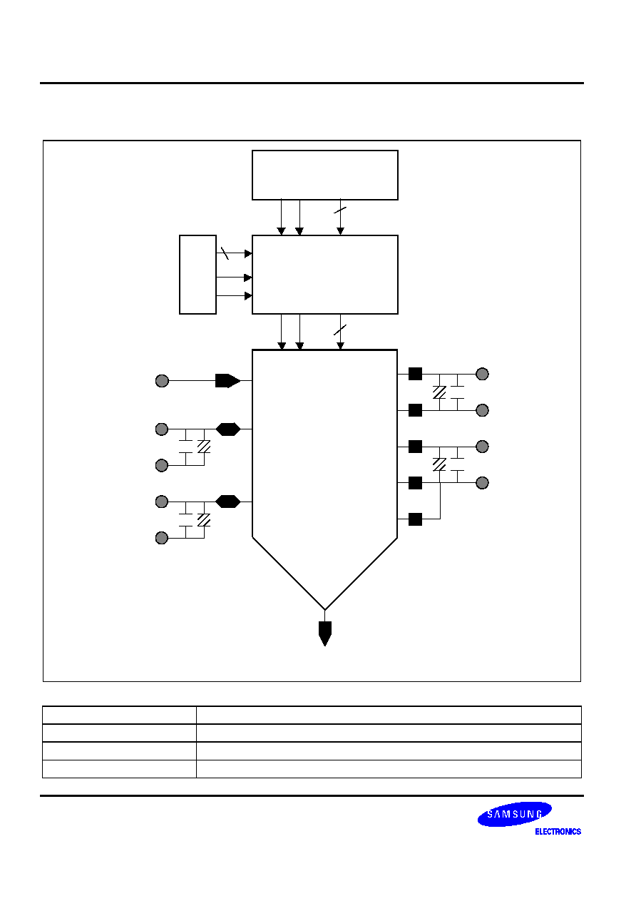
FUNCTIONAL BLOCK DIAGRAM
D[9:0]
R-2R Ladder
VRB
VRT
VOUT
PWRDN
VDDD
VSSD
VDDA
VSSA
VBBA
OP
AMP
_
+
Switch
DACCON
EXTREF
0.35
µ
µ
µ
µ
m 3.3 V 10-BIT 0.5MSPS DAC
BW1244D
3
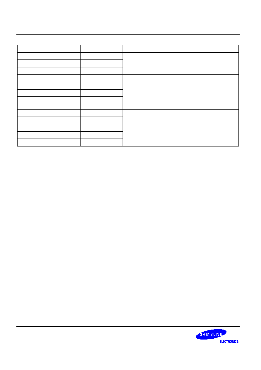
CORE PIN DESCRIPTION
Name
I/O Type
I/O Pad
Pin Description
D[9:0]
DI
picc_bb
Digital Input Data (10bit)
D[9] : MSB , D[0] : LSB
EXTREF
AI
pia_bb
External Reference
DACCON
DI
picc_bb
OP Amp Input Control
High : Amp In Æ EXTREF
Low : Amp In Æ R2R Output
PWRDN
DI
picc_bb
Power Down (Active Low)
VRT
AB
pia_bb
Voltage Reference Top
VRB
AB
pia_bb
Voltage Reference Bottom
VOUT
AO
poa_bb
Analog Voltage Output
VDDD
DP
vddd
Digital Power (+3.3V)
VSSA
DG
vssd
Digital Ground (0.0V)
VDDA
AP
vdda
Analog Power (+3.3V)
VSSA
AG
vssa
Analog Ground (0.0V)
VBBA
AG
vbba
Analog Sub Bias (0.0V)
I/O Type Abbr.
-- AI: Analog Input
-- DI: Digital Input
-- AO: Analog Output
-- DO: Digital Output
-- AB: Analog Bidirectional
-- DB: Digital Bidirectional
-- AP: Analog Power
-- DP: Digital Power
-- AG: Analog Ground
-- DG: Digital Ground

BW1244D
0.35
µ
µ
µ
µ
m 3.3 V 10-BIT 0.5MSPS DAC
4
CORE CONFIGURATION
VRT
VRB
D[9:0]
VOUT
VDDD
VSSD
VDDA
VSSA
VBBA
PWRDN
bw1244d
EXTREF
DACCON
0.35
µ
µ
µ
µ
m 3.3 V 10-BIT 0.5MSPS DAC
BW1244D
5
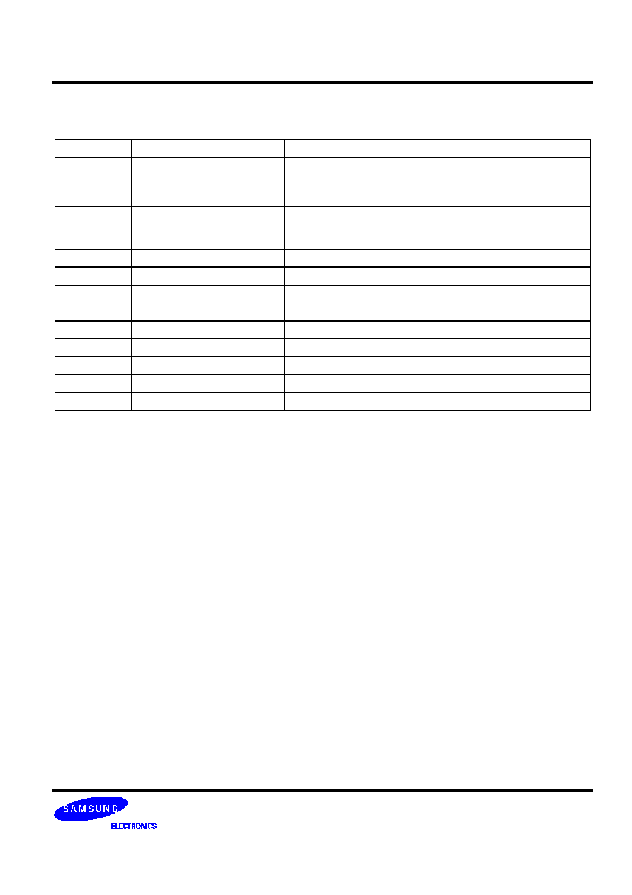
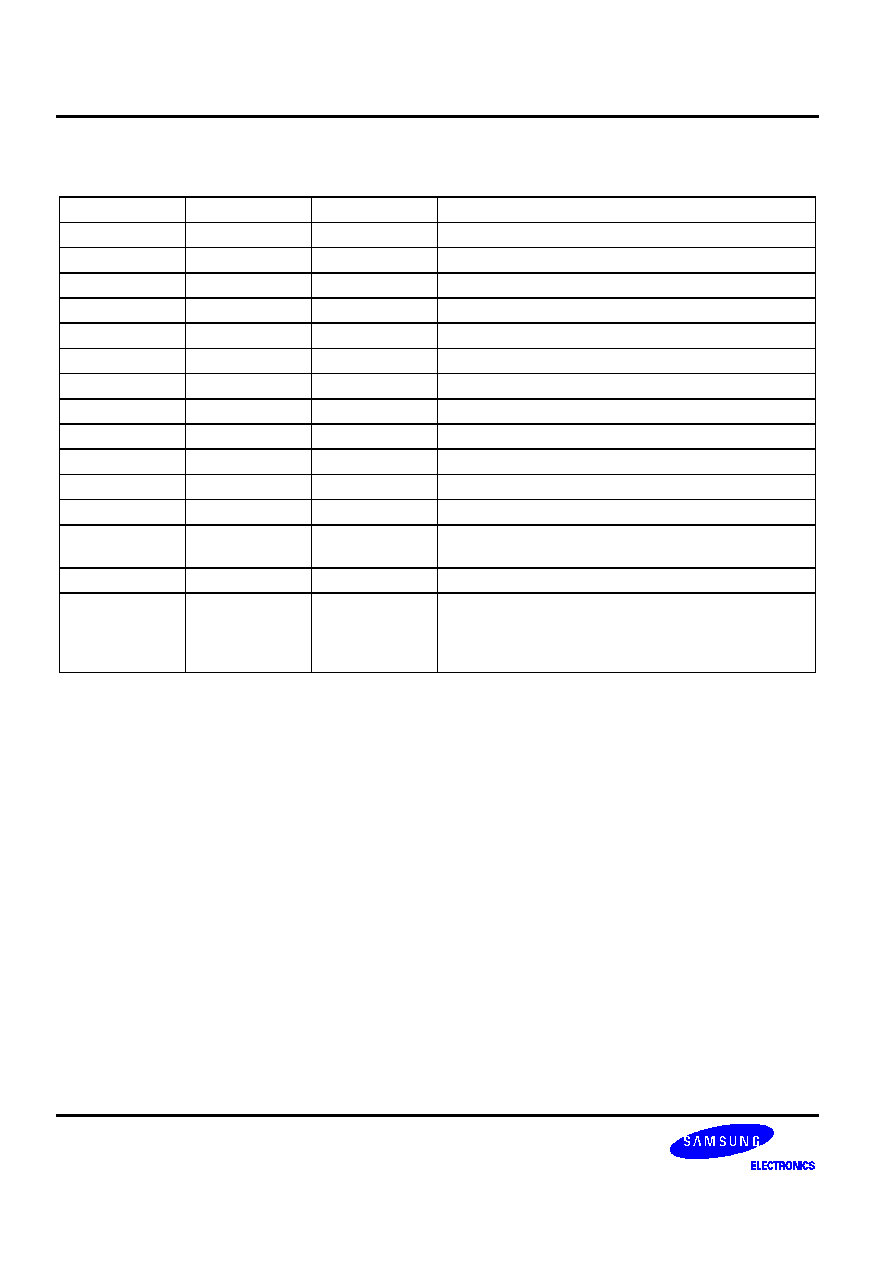
ABSOLUTE MAXIMUM RATINGS
Characteristics
Symbol
Value
Unit
Supply Voltage
VDD (VDDA,VDDD)
4.5
V
Analog Output Voltage
VOUT
VSS to VDD
V
Digital Input Voltage
D[9:0]
VSS to VDD
V
Reference Voltage
VRT
VRB
VDD
VSS
V
Operating Temperature Range
Topr
0 to 70
∞
C
NOTES :
1.
ABSOLUTE MAXIMUM RATING specifies the values beyond which the device may be damaged permanently.
Exposure to ABSOLUTE MAXIMUM RATING conditions for extended periods may affect reliability. Each condition
value is applied with the other values kept within the following operating conditions and function operation under any
of these conditions is not implied.
2.
All voltages are measured with respect to VSS(VSSA or VSSD or VBBA) unless otherwise specified.
3.
100pF capacitor is discharged through a 1.5k
resistor (Human body model)
RECOMMENDED OPERATING CONDITIONS
Characteristics
Symbol
Min
Typ
Max
Unit
Supply Voltage
VDDA - VSSA
VDDD - VSSD
3.15
3.3
3.45
V
Supply Voltage Difference
VDDA - VDDD
-0.1
0.0
0.1
V
Reference Voltage
VRT
VRB
-
0.0
-
-
3.3
-
V
Digital Input 'Low' Voltage
Digital Input 'High' Voltage
VIL
VIH
-
0.7¥VDD
-
-
0.3¥VDD
-
V
Operating Temperature
Topr
0
-
70
∞C
NOTE: It is strongly recommended that to avoid power latch-up all the supply pins(VDDA,VDDD) be driven from the same
source.
BW1244D
0.35
µ
µ
µ
µ
m 3.3 V 10-BIT 0.5MSPS DAC
6
DC ELECTRICAL CHARACTERISTICS
(Converter Specifications : VDDA=VDDD=3.3V, VSSA=VSSD=VBBA=0V, PWRDN=High, Top=25∞C, VRT=3.3V,
VRB=0.0V unless otherwise specified.)
Characteristics
Symbol
Min
Typ
Max
Unit
Conditions
Resolution
Bit
-
-
10
Bits
-
Differential Linearity Error
DLE
-
0.3
0.5
LSB
-
Integral Linearity Error
ILE
-
1.5
2.0
LSB
-
Zero Scale Error
1
V
ZSE
-
3
6
mV
VRT=3.3V , VRB=0.0V
Full Scale Voltage Error
2
V
FSE
-
4
11
mV
Maximum Output Voltage
Vo
MAX
3.280
3.290
3.297
V
Vo
MAX
= VOUT(D[9:0]=High)
V
LSB
= Vo
MAX
/ 1023
LSB Size
V
LSB
3.206
3.220
3.223
mV
EOT = VRT - AIN(254,255)
NOTES:
1.
V
ZSE
=VOUT(D[9:0]=Low) - VRB
2.
V
FSE
=VOUT(D[9:0]=High) - {(VRT-VRB) ¥ 1023/1024 + VRB}

0.35
µ
µ
µ
µ
m 3.3 V 10-BIT 0.5MSPS DAC
BW1244D
7
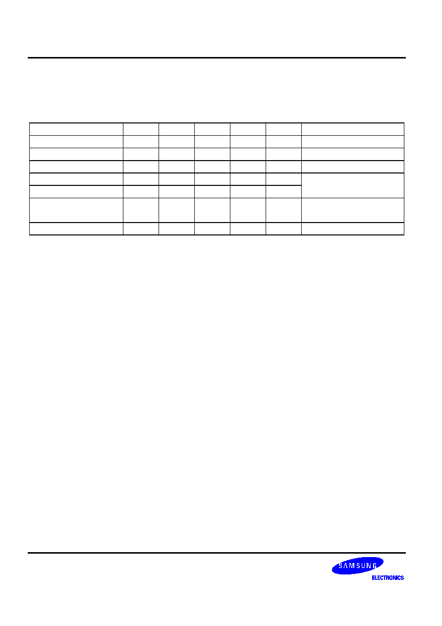
AC ELECTRICAL CHARACTERISTICS
(Converter Specifications : VDDA=VDDD=3.3V, VSSA=VSSD=VBBA=0V, load cap=25pF, Top=25∞C, VRT=3.3V,
VRB=0.0V unless otherwise specified.)
Characteristics
Symbol
Min
Typ
Max
Unit
Conditions
Maximum
Conversion Rate
f
C
-
-
0.5
MSPS
Data Rate = 0.5MHz
Dynamic Supply Current
Ivdd1
-
3
-
mA
Ivdd1 = I
VDDA
+ I
VRT
+ I
VDDD
Data Rate = 0.5MHz
Dynamic Supply Current
(Power Down Mode)
Ivdd2
-
-
10
uA
Ivdd2 = I
VDDA
+ I
VDDD
Data Rate = 0.5MHz
PWRDN=LOW
Analog Output Delay
Td
90
100
105
ns
Data Rate = 0.5MHz
Data : All LOW ÆAll HIGH
Analog Output Rise Time
Tr
100
107
115
ns
Data Rate = 0.5MHz
Data : All LOW Æ All HIGH
Analog Output Fall Time
Tf
94
100
107
ns
Data Rate = 0.5MHz
Data : All HIGH Æ All LOW
Analog Output
Settling Time
Ts
160
240
350
ns
Data Rate = 0.5MHz
Data : All LOW Æ All HIGH
VRT = VDD/2
Power Down On Time
Ton
50
53
60
ns
PWRDN : HIGH Æ LOW
Power Down Off Time
Toff
155
165
180
ns
PWRDN : LOW Æ HIGH
External Reference
Transition On Time
Texon
-
0.5
0.8
us
DACCON : LOW Æ HIGH
Amp In = EXTREF
External Reference
Transition Off Time
Texoff
-
0.5
0.8
us
DACCON : HIGH Æ LOW
Amp In = R2R Ladder Output
BW1244D
0.35
µ
µ
µ
µ
m 3.3 V 10-BIT 0.5MSPS DAC
8
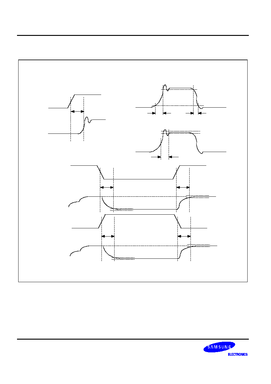
TIMING DIAGRAM
DATA
VOUT
Td
0000000000
1111111111
50%
50%
VOUT
0000000000
1111111111
0000000000
10%
90%
DATA
Tr
Tf
VOUT
0000000000
1111111111
0000000000
50%
± 0.5LSB
DATA
Ts
PWRDN
VOUT
Ton
50%
Toff
50%
± 0.5LSB
± 0.5LSB
0.0V
DACCON
VOUT
Texon
50%
Texoff
50%
± 0.5LSB
± 0.5LSB
EXTREF
1. Output delay measured from the 50% point of the rising edge of input data to the full scale transition.
2. Settling time measured from the 50% point of full scale transition to the output remaining within ±1/2 LSB.
3. Output rise/fall time measured between the 10% and 90% points of full scale transition.

0.35
µ
µ
µ
µ
m 3.3 V 10-BIT 0.5MSPS DAC
BW1244D
9
FUCTION DESCRIPTION
1. The bw1244d has a R-2R Ladder Block for 10bit and an OP amp Block for driving Output.
2. The R-2R Ladder Block generates binary weighted voltage (VRT/21 , VRT/22 , VRT/23 , ... VRT/210)
corresponding to Digital Input Data for n-bit DAC and Output total voltage is summing of each values.
3. In Output voltage, VMSB = VRT/21
VLSB = VRT/210
4. Output of the R-2R Ladder Block is driven by OP amp.
5. The DACCON signal controls OP amp input. When DACCON is low, the bw1244d operates normally so R-2R
Ladder output drives OP amp input But when DACCON is high, OP amp input is connected to EXTREF, so
bw1244d output is buffered signal of EXTREF.
6. In power down mode, only analog current (I
VDDA
) is reduced.
BW1244D
0.35
µ
µ
µ
µ
m 3.3 V 10-BIT 0.5MSPS DAC
10
CORE EVALUATION GUIDE
MUX
TEST
PAT
H
10
10
10
Cc
Ct
VDDD
VSSD
VDDA
VSSA
VBBA
3.
3V
G
N
D
3
.
3
V
G
N
D
Cc
Ct
Ct
Cc
Ct
Cc
3.
3V
G
N
D
0
.
0
V
G
N
D
D[
9:
0]
PWRD
N
VRT
V
RB
VOU
T
bw1
244d
VOU
T
DACC
ON
EXTREF
An
al
o
g
In
pu
t
HO
ST
DSP
CO
RE
Location
Description
Ct
10uF TANTALUM CAPACITOR
Cc
0.1uF CERAMIC CAPACITOR
L1~L5
FERRITE BEAD ( 0.1mh )

0.35
µ
µ
µ
µ
m 3.3 V 10-BIT 0.5MSPS DAC
BW1244D
11
TESTABILITY
Whether you use MUX or the internal logic for testability, it is required to be able to select values of digital inputs
(D[9:0]). above figure. Only if it is, you can check the main function. (Linearity) Test Condition: VRT=3.3V,
VRB=0.0V, PWRDN=High, DACCON=Low.
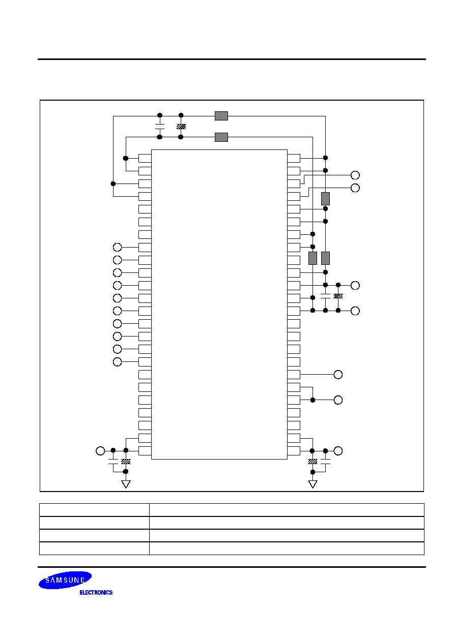
CORE LAYOUT GUIDE
bw1244x
D[9]
DACCON
EXTREF
VOUT
D[8]
D[7]
D[6]
D[5]
D[4]
D[3]
D[2]
D[1]
D[0]
VDDD
V
SSD
VBBA
VDDA
V
SSA
VBBA
bw1244x
D[9]
DACCON
EXTREF
VOUT
D[8]
D[7]
D[6]
D[5]
D[4]
D[3]
D[2]
D[1]
D[0]
VRB
VRT
VDDD
V
SSD
VBBA
VDDA
V
SSA
VBBA
BW1244D
0.35
µ
µ
µ
µ
m 3.3 V 10-BIT 0.5MSPS DAC
12
Pin Name
Property
Pin Usage
Pin Layout Guide
D[9:0]
DI
Internal / External
1. Digital Input Signal lines must have same length to
DACCON
DI
Internal / External
reduce propagation delay.
PWDNB
DI
Internal / External
VRT
AB
External
1. Voltage reference lines (VRT and VRB) must be wide
VRB
AB
External
metal to reduce voltage drop of metal lines.
EXTREF
AI
Internal / External
2. VOUT signal should not be crossed by any signals and
VOUT
AO
Internal / External
should not run next to digital signals to minimize
apacitive coupling between the two signals.
VDDA
AP
External
1. It is recommended that you use thick analog power
VSSA
AG
External
metal. When connected to PAD, the path should be
VDDD
DP
External
kept as short as possible.
VSSD
DG
External
2. Digital power and analog power are separately used.
VBBA
AG
External
1. When the core block is connected to other blocks, it must be double guard-ring using N-well and P+ active
to remove the substrate and coupling noise.
In that case, the power metal should be connected to PAD directly.
2. The Bulk power is used to reduce the influence of substrate noise.
0.35
µ
µ
µ
µ
m 3.3 V 10-BIT 0.5MSPS DAC
BW1244D
13
PACKAGE CONFIGURATION
VRB
1
2
3
4
5
6
7
8
9
10
11
12
13
14
15
16
17
18
19
20
21
22
23
24
48
47
46
45
44
43
42
41
40
39
38
37
36
35
34
33
32
31
30
29
28
27
26
25
VDDD
VDDD
VSSD
VSSD
NC
NC
NC
D[9]
D[8]
D[7]
D[6]
D[5]
D[4]
D[3]
D[2]
D[1]
D[0]
NC
NC
NC
NC
NC
VRB
VRB
VBBA
VBBA
DACCON
EXTREF
VSSZ
VSSZ
VDDZ
VDDZ
NC
VSSA
VSSA
VDDA
VDDA
NC
NC
NC
NC
PWRDN
VOUT
VOUT
NC
NC
VRT
VRT
Cc
Ct
L1
L2
Cc
Ct
+
+
0.0V
3.3V
(VSS)
(VDD)
+
Ct
Cc
PWRDN
VOUT
VRT
(3.3V Typ.)
(3.3V in normal operation)
Ct
+
Cc
(0.0V Typ.)
D[9]
D[8]
D[7]
D[6]
D[5]
D[4]
D[3]
D[2]
D[1]
D[0]
L3
L5
L4
EXTREF
DACCON
B
W
1244D
VRB
1
2
3
4
5
6
7
8
9
10
11
12
13
14
15
16
17
18
19
20
21
22
23
24
48
47
46
45
44
43
42
41
40
39
38
37
36
35
34
33
32
31
30
29
28
27
26
25
VDDD
VDDD
VSSD
VSSD
NC
NC
NC
D[9]
D[8]
D[7]
D[6]
D[5]
D[4]
D[3]
D[2]
D[1]
D[0]
NC
NC
NC
NC
NC
VRB
VRB
VBBA
VBBA
DACCON
EXTREF
VSSZ
VSSZ
VDDZ
VDDZ
NC
VSSA
VSSA
VDDA
VDDA
NC
NC
NC
NC
PWRDN
VOUT
VOUT
NC
NC
VRT
VRT
Cc
Ct
L1
L2
Cc
Ct
+
+
0.0V
3.3V
(VSS)
(VDD)
+
Ct
Cc
PWRDN
VOUT
VRT
(3.3V Typ.)
(3.3V in normal operation)
Ct
+
Cc
(0.0V Typ.)
D[9]
D[8]
D[7]
D[6]
D[5]
D[4]
D[3]
D[2]
D[1]
D[0]
L3
L5
L4
EXTREF
DACCON
B
W
1244D
Location
Description
Ct
10uF TANTALUM CAPACITOR
Cc
0.1uF CERAMIC CAPACITOR
L1~L5
FERRITE BEAD ( 0.1mh )
BW1244D
0.35
µ
µ
µ
µ
m 3.3 V 10-BIT 0.5MSPS DAC
14
PACKAGE PIN DESCRIPTION
Name
Pin No
I/O Type
Pin Description
VDDD
1,2
DP
Digital Power (3.3V)
VSSD
3,4
DG
Digital Ground (0.0V)
D[9:0]
8~17
DI
Digital Input Data
VRB
23,24
AB
Voltage Reference Bottom (0.0V)
VRT
25,26
AB
Voltage Reference Top (3.3V)
VOUT
29,30
AO
Analog Voltage Output
PWRDN
31
DI
Power Down Mode (Low Active)
VDDA
36,37
AP
Analog Power (3.3V)
VSSA
38,39
AG
Analog Ground (0.0V)
VDDZ
41,42
AP
Pad Power (3.3V)
VSSZ
43,44
AG
Pad Ground (0.0V)
EXTREF
45
AI
External Reference
DACCON
46
DI
DAC Control (Low : DAC Normal Operation)
(High : Output is buffered EXTREF)
VBBA
47,48
AG
Analog Sub Bias (0.0V)
NC
5,6,7,18,19
20,21,22,27
28,32,33,34
35,40
DO
No Connection
I/O Type Abbr.
-- AI: Analog Input
-- DI: Digital Input
-- AO: Analog Output
-- DO: Digital Output
-- AB: Analog Bidirectional
-- DB: Digital Bidirectional
-- AP: Analog Power
-- DP: Digital Power
-- AG: Analog Ground
-- DG: Digital Ground

0.35
µ
µ
µ
µ
m 3.3 V 10-BIT 0.5MSPS DAC
BW1244D
15
PC BOARD LAYOUT CONSIDERATION
1. PC Board Considerations
To minimize noise on the power lines and the ground lines, the digital inputs to be shielded and decoupled. This
trace length between groups VDD (VDDA,VDDD) and VSS (VSSA,VSSD) pins should be as short as possible as
to minimize inductive ringing.
2. Supply Decoupling and Planes
For the decoupling capacitor between the power line and the ground line, 0.1uF capacitor is used in parallel with a
10uF tantalum capacitor. digital power plane(VDDD) and analog power plane(VDDA) are connected a ferrite bead,
and also the digital ground plane(VSSD) and the analog plane(VSSA). This ferrite bead should be located within
3inches of BW1244D. The analog power plane supplies power to the BW1244D of analog output pin and related
devices.
BW1244D
0.35
µ
µ
µ
µ
m 3.3 V 10-BIT 0.5MSPS DAC
16
FEEDBACK REQUEST
We appreciate your interest in out products. If you have further questions, please specify in the attached form you
very much.
DC / AC ELECTRICAL CHARACTERISTIC
Characteristics
Min
Typ
Max
Unit
Remarks
Supply Voltage
V
Power dissipation
mW
Resolution
Bits
Analog Output Voltage
V
Operating Temperature
∞C
Output Load Capacitor
pF
Output Load Resistor
k
Integral Non-Linearity Error
LSB
Differential Non-Linearity Error
LSB
Maximum Conversion Rate
MHz
VOLTAGE OUTPUT DAC
Reference Voltage TOP
BOTTOM
V
Analog Output Voltage Range
V
Digital Input Format
Binary Code or 2's Complement Code
CURRENT OUTPUT DAC
Analog Output Maximum Current
mA
Analog Output Maximum Signal Frequency
kHz
Reference Voltage
V
External Resistor for Current Setting(RSET)
Pipeline Delay
sec
-- Do you want to Power down mode?
-- Do you want to Internal Reference Voltage(BGR)?
-- Which do you want to serial input data type or parallel input data type?
-- Do you need 3.3V and 5V power supply in your system?

0.35
µ
µ
µ
µ
m 3.3 V 10-BIT 0.5MSPS DAC
BW1244D
17
HISTORY CARD
Version
Date
Modified Items
Comments
Ver 1.5
00.02.22
Version updated
All pictures and texts are modified with dac1236x's datasheet.
The format ant fonts of datasheet are same with dac1236x's
datasheet.
Reference
datasheet
DAC1236X
Ver 1.6
01.03.28
Version Updated
page 4 : power down mode current (
10uA)
page 11 :
∞
C
k
(Output Load Resistor)
Ver 1.7
02.04.23
Version Updated
page 5 : functional description is modified.
page 6 : functon
function
page 7 : phantom cell is modified and table is added.
page 8 : VRT pin number is modified (18
25)
page 11 : W

BW1244D
0.35
µ
µ
µ
µ
m 3.3 V 10-BIT 0.5MSPS DAC
18
NOTES