 | –≠–ª–µ–∫—Ç—Ä–æ–Ω–Ω—ã–π –∫–æ–º–ø–æ–Ω–µ–Ω—Ç: bw2017x | –°–∫–∞—á–∞—Ç—å:  PDF PDF  ZIP ZIP |

0.35
µ
µ
µ
µ
m 3MHZ-25MHZ FSPLL
BW2017X
1
GENERAL DESCRIPTION
BW2017X is a Phase-Locked Loop (PLL) frequency synthesizer implemented in 0.35um CMOS technology.
The PLL provides frequency multiplication capability. The output clock frequency Fout is related to the reference
input clock frequency Fin by the following equation:
Fout
M Fin
P S
=
◊
◊
where
Fout : output clock frequency.
Fin : reference input clock frequency.
M, P and S : values of programmable dividers.
BW2017X consists of a phase and frequency detector(PFD), a charge pump, an external loop filter, a voltage
controlled oscillator(VCO), a 4bit pre-divider P, an 8bit main divider M and a 2bit post scaler S, and a lock detector
as shown in Figure1.
FEATURES
-- 0.35um CMOS technology
-- 3.3V Single power supply
-- Output frequency range: 3 ~ 25MHz
-- Cycle Jitter: ±300ps
-- Duty ratio: 40% ~ 60%
-- Frequency change by programmable divider
-- Power down mode
IMPORTANT NOTICE
Please contact SEC application engineer to confirm the proper selection of M,P,S value.

BW2017X
0.35
µ
µ
µ
µ
m 3MHZ-25MHZ FSPLL
2
FUNCTIONAL BLOCK DIAGRAM
charge
pump
PFD
VCO
Main
divider
M
Post
scaler
S
Loop
Filter
(external)
Pre
divider
P
Fin
Fout
Filter
Figure 1. BW2017X Block Diagram

0.35
µ
µ
µ
µ
m 3MHZ-25MHZ FSPLL
BW2017X
3
CORE PIN DESCRIPTION
Name
I/O Type
I/O Pad
Pin Description
VDD
DP
vddd
Digital power supply
VSS
DG
vssd
Digital ground
VDDA
AP
vdda
Analog power supply
VSSA
AG
vssa
Analog ground
VBB
AB/DB
vbba
Analog / Digital Sub Bias
FIN
DI
picc_bb
PLL clock input
FOUT
DO
pot12_bb
3 ~ 25MHz clock output
FILTER
DO
poar50_bb
- Charge pump output is connected to loop filter.
- A capacitor is connected between the pin and analog
ground.
PWD
DI
picc_bb
FSPLL clock power down.
- PWD is active HIGH.
- If NOT used, tie it to VSSD.
P[3:0]
DI
picc_bb
The values for 4bit programmable pre-divider.
M[7:0]
DI
picc_bb
The values for 8bit programmable main divider.
S[1:0]
DI
picc_bb
The values for 2bit programmable post scaler.
I/O Type Abbr.
-- AI: Analog Input
-- DI: Digital Input
-- AO: Analog Output
-- DO: Digital Output
-- AB: Analog Bidirectional
-- DB: Digital Bidirectional
-- AP: Analog Power
-- DP: Digital Power
-- AG: Analog Ground
-- DG: Digital Ground

BW2017X
0.35
µ
µ
µ
µ
m 3MHZ-25MHZ FSPLL
4
CORE CONFIGURATION
¢∫
°·
¢∫
°·
¢∫
°·
FIN
PWD
FOUT
bw2017x
M[0]
M[1]
M[2]
M[3]
M[4]
M[5]
M[6]
M[7]
P[0]
P[1]
P[2]
P[3]
S[0]
S[1]
¢∫
°·
¢∫
°·
¢∫
°·
M[7:0]
P[3:0]
S[1:0]
¢∫
°·
FILTER
0.35
µ
µ
µ
µ
m 3MHZ-25MHZ FSPLL
BW2017X
5
ABSOLUTE MAXIMUM RATINGS
Characteristics
Symbol
Value
Unit
Applicable pin
Supply Voltage
VDD
VDDA
-0.3 to 3.8
V
VDD,VSS
VDDA,VSSA,VBB
Voltage on any digital pin
Vin
VSS-0.3 to VDD+0.3
V
P[3:0],M[7:0],S[1:0], PWD
Storage Temperature
Tstg
-45 to 125
°…
-
NOTES:
1.
ABSOLUTE
MAXIMUM RATINGS specify the values beyond which the device may be damaged permanently.
Exposure to ABSOLUTE MAXIMUM RATINGS conditions for extended periods may affect reliability.
Each condition value is applied with the other values kept within the following operating conditions and function
operation under any of these conditions is not implied.
2. All voltages are measured with respect to VSS unless otherwise specified.
3. 100pF
capacitor
is
discharged
through
a
1.5ß⁄
resistor
(Human
body
model)
RECOMMENDED OPERATING CONDITIONS
Characteristics
Symbol
Min
Typ
Max
Unit
Supply Voltage Differential
VDD - VDDA
-0.1
0.1
V
External Loop Filter Capacitance
L
F
940
pF
Operating Temperature
Topr
0
70
°…
NOTE: It is
strongly
recommended
that
all
the
supply
pins
(VDDA,
VDD)
be
powered
from
the
same
source
to
avoid
power
latch-up.
BW2017X
0.35
µ
µ
µ
µ
m 3MHZ-25MHZ FSPLL
6
DC ELECTRICAL CHARACTERISTICS
Characteristics
Symbol
Min
Typ
Max
Unit
Operating Voltage
VDD,VDDA
3.15
3.3
3.45
V
Digital Input Voltage High
VIH
2.0
V
Digital Input Voltage Low
VIL
0.8
V
Dynamic Current
(CORE Level without I/O Cell)
Idd
2
mA
Power Down Current
Ipd
50
uA
AC ELECTRICAL CHARACTERISTICS
Characteristics
Symbol
Min
Typ
Max
Unit
Input Frequency
F
IN
4
MHz
Output Clock Frequency
F
OUT
3
25
MHz
VCO Output Clock Frequency
Fvco
3
25
MHz
Input Clock Duty Cycle
T
ID
40
60
%
Output Clock Duty Cycle (at 25MHz)
T
OD
40
60
%
Lock Time
T
LT
300
us
Cycle to Cycle Jitter
T
JCC
-300
+300
ps
0.35
µ
µ
µ
µ
m 3MHZ-25MHZ FSPLL
BW2017X
7
FUNCTION DESCRIPTION
A PLL is the circuit synchronizing an output signal (generated by an VCO) with a reference or input signal in
frequency as well as in phase.
In this application, it includes the following basic blocks.
∑
The voltage-controlled oscillator to generate the output frequency
∑
The pre-divider P divides the reference frequency by P.
∑
The main divider M divides the VCO output frequency by M.
∑
The post scaler S divides the VCO output frequency by S.
∑
The phase and frequency detector (PFD) detects the phase and frequency difference between the reference
input and VCO output (after M division) and controls the charge pump current.
∑
The loop filter removes high frequency components in VCO control voltage and does smooth and correct
control of VCO.
∑
The M, P, and S values can be programmed by 14bit digital data from the external source. Thus the PLL can
be locked onto the desired frequency.
Fout
M Fin
P S
=
◊
◊
If Fin = 4MHz, and M=m+8 , P=p+2, S=2^s
Digital data format:
Main Divider
Pre Divider
Post Scaler
M7,M6,M5,M4,M3,M2,M1,M0
P3,P2,P1,P0
S1,S0
NOTES:
1.
S1 - S0: Output Frequency Scaler
2.
M7 - M0: VCO Frequency Divider
3.
P3 - P0: Reference Frequency Input Divide
NOTES
1. Don't set the P or M as zero, that is 000000 / 00000000
2. The proper range of P and M : 1<=P<=14, 1<=M<=248
3. The P and M must be selected considering stability of PLL and VCO output frequency range
4. Please consult with SEC application engineer to select the proper P, M and S values
BW2017X
0.35
µ
µ
µ
µ
m 3MHZ-25MHZ FSPLL
8
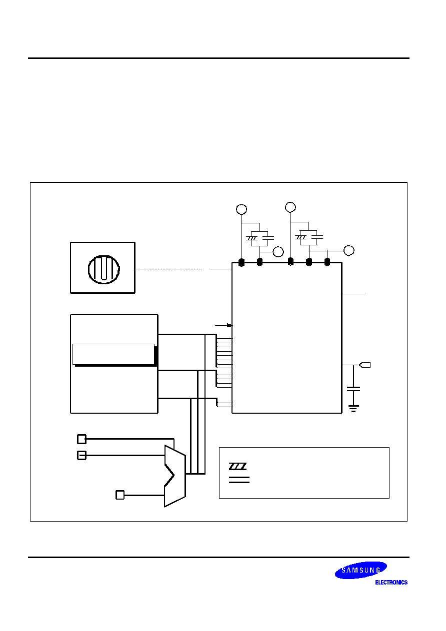
CORE EVALUATION GUIDE
For an embedded PLL, we must consider test circuit for the embedded core in multiple applications.
Hence the following requirements should be satisfied.
-- FOUT pin must be bypassed for external test.
-- For the PLL test (below two examples), it is needed to control the dividers - M[7:0],P[3:0] and S[1:0] -that
generate multiple frequencies. Example #1. Registers can be used for easy control of divider values.
Example #2. N sample bits of 14-bit divider pins can be bypassed for test using MUX.
NOTE:
: 10uF ELECTROLYTIC CAPACITOR
UNLESS OTHERWISE SPECIFIED
: 0.1 CERAMIC CAPACITOR
UNLESS OTHERWISE SPECIFIED
¢∫
°·
FOUT
FILTER
bw2017x
#1. 14bit Register
Block
PWD
P[3:0]
S[1:0]
940pF
M[7:0]
¢∫
°·
FIN
External Clock Source
VDD
VSS
VDDA VSSA
3.3V
Digital
Power
3.3V Analog Power
GND
GND
VSSA
Select Pin
Test Pins of N Sample bits
Internal Divider Signal Line
#2
M
U
X
Figure 3. BW2017X Core Test Scheme

0.35
µ
µ
µ
µ
m 3MHZ-25MHZ FSPLL
BW2017X
9
CORE LAYOUT GUIDE
-- The digital power(VDD,VSS) and the analog power(VDDA,VSSA) must be dedicated only to PLL and be
seperated. If the dedicated VDD and VSS is not available, that of the least power consuming block is shared
with the PLL.
-- The POA pad is used as a FILTER pad that contains ESD protection diodes without any resistors and buffers.
-- The FOUT and FILTER pins must be placed far from the internal signals in order to prevent them from
overlapping signal lines.
-- The blocks having a large digital switching current must be located away from the PLL core.
-- The PLL core must be shielded by guard ring.
-- For the FOUT, you can use a custom drive buffer or POT12 buffer considering the drive current.
WITHOUT XTAL-DRIVER USERS GUIDE
-- There are two crystal driver cell (XTAL-OSC and PSOSCM2) options for the BW2017X PLL core.
1. If the crystal component not used , an external clock source is applied to the FIN
* Please contact an SEC application engineer when using a crystal.
2. If the crystal component not used , an external clock I/O Buffer offered from Samsung's STD90 library is
recommanded for use
- When implementing an embedded PLL block, the following pins must be bypassed externally for testing
the PLL locking function:
* Without Xtal-driver : FIN,FILTER,FOUT,VDDA,VSSA,VDD and VSS.

BW2017X
0.35
µ
µ
µ
µ
m 3MHZ-25MHZ FSPLL
10
VDD
°·
VSSA
MUX
°·
°·
FOUT
°·
FILTER
Divider
P
PFD
&CP
LF
VCO
Divider
M
VSS
VDDA
Glue Logic
FIN
PWRDN
Scaler
S
Used PICC_BB PAD
°·
°·
°·
°·
S[1:0]
M[7:0]
P[3:0]
VBBA
°·
* Optional Test Pins
* Divider Bus
Figure 2. The example of PLL block without crystal component (Normal Case)

0.35
µ
µ
µ
µ
m 3MHZ-25MHZ FSPLL
BW2017X
11
PACKAGE CONFIGURATION
2
1
4
3
6
5
8
7
10
9
12
11
35
36
33
34
31
32
29
30
27
28
25
26
13
14
15
16
17
18
19
20
21
23
24
48
47
46
45
44
43
42
41
40
39
38
37
22
N
C
N
C
V
S
S
A
VDDA
VDDA
FIN
FILTER
NC
FOUT
NC
N
C
V
S
S
O
V
D
D
O
S
0
S
1
N
C
V
S
S
D
V
D
D
D
V
D
D
D
M0
M1
M2
M3
M4
M5
M6
M7
P0
P1
P2
P3
bw2017x
C
10uF
103
C
C
L
H
L
H
L
H
L
H
L
H
L
H
L
H
L
H
L
H
L
H
L
H
L
H
L
H
940pF
4bit Pre Divider Input
Dummy Test Block Control pins
3.3V Digital PAD Power
3.3V Analog Power
2bit Post Scaler
8bit Main Divider
N
C
N
C
N
C
N
C
N
C
N
C
N
C
V
S
S
A
PWD
VBBA
V
S
S
D
C
L
H
L
H
L
H
L
H
L
H
3.3V I/O Power
L
H
LD
NC
External Clock Source
VBBA
N
C
N
C
N
C
NOTES:
1.
NC is Noconnection pin
2.
LD is test pin of SEC
BW2017X
0.35
µ
µ
µ
µ
m 3MHZ-25MHZ FSPLL
12
PACKAGE PIN DESCRIPTION
Name
Pin No
I/O Type
Pin Description
VDDD
35,36
DP
Digital power supply
VSSD
33,34
DG
Digital ground
PWD
18
DI
FSPLL clock power down
- PWRDN is High, PLL do not operating under this
condition.
- If isn't used this pin, tied to VSS.
P[0]~P[3]
45~48
DI
Pre-Divider Input(LSB)
VDDA
13,14
AP
Analog power supply
VSSA
11,12
AG
Analog ground
VBBA
19,20
AB/DB
Analog / Digtal Sub Bias Power
FIN
15
AI
Crystal input or external F
REF input
FOUT
22
DO
3MHZ~25MHz clock output
FILTER
17
AO
Pump out is connected to the FILTER.
A 940pF Capcitor is connected between the pin and
analog pin
S[0]~S[1]
31,32
DI
Post scaler input
M[0]~M[7]
37~44
DI
8bit main divider input
VDDO
28
PP
I/O PAD Power
VSSO
27
PG
I/O PAD Ground
NOTE: I/O
TYPE
PP
and
PG
denote
PAD
power
and
PAD
ground
respectively.

0.35
µ
µ
µ
µ
m 3MHZ-25MHZ FSPLL
BW2017X
13
DESIGN CONSIDERATIONS
The following design considerations apply :
-- Phase tolerance and jitter are independent of the PLL frequency.
-- Jitter is affected by the noise frequency in the power(VDD,VSS,VDDA, and VSSA).
It increases when the noise level increases.
-- A CMOS-level input reference clock is recommended for signal compatibility with the PLL circuit. Other levels
such as TTL and ECL may degrade the tolerances.
-- The use of two or more PLLs requires special design considerations. Please contact your application engineer
for the detail.
-- The following apply to the noise level, which can be minimized by selecting good analog power and ground
isolation techniques in the system:
- Use wide PCB traces for POWER(VDD,VSS, VDDA, and VSSA) connections to the PLL core. Seperate
the traces from the chips' VDD/VSS/VDDA/VSSA supplies.
- Use proper VDD/VSS/VDDA/VSSA decoupling method.
- Use good power and ground sources on the board.
- Use bulk power VBB to minimize substrate noise.
-- The PLL core should be placed as close as possible to the dedicated loop filter and analog Power and
ground pins.
-- It is not desirable to put it close to the noise-generating signals such as data buses and high-current outputs
near the PLL I/O cells.
-- Other related I/O signals should be placed near the PLL I/O but do not have any pre-defined placement
restriction.
BW2017X
0.35
µ
µ
µ
µ
m 3MHZ-25MHZ FSPLL
14
FEEDBACK REQUEST
Thank you for having an interest in our products. Please fill out this form, especially the items which you want to
request.
Parameter
Customer
SEC
Unit
Process
Supply voltage (VDD)
Input frequency (FIN)
Output frequency (FOUT)
Cycle to cycle jitter (TJCC)
100M ~ 200M
200M ~ 300M
300M ~ 400M
400M ~ 500M
Period jitter (TJP)
100M ~ 200M
200M ~ 300M
300M ~ 400M
400M ~ 500M
Output duty ratio (TOD)
Lock up time (TLT)
Dynamic current
Stand by current
Filter capacitor
-- How many PLLs are embedded in your system ?
-- Do you need synchronization between input clock and output clock ?
-- Do you need another spec of jitter ?
Parameter
Customer
Unit
Long-term jitter (TJLT)
psec (pk-pk)
Tracking Jitter (TJT)
psec (pk-pk)
If you have another special request, please describe below.
0.35
µ
µ
µ
µ
m 3MHZ-25MHZ FSPLL
BW2017X
15
JITTER DEFINITION
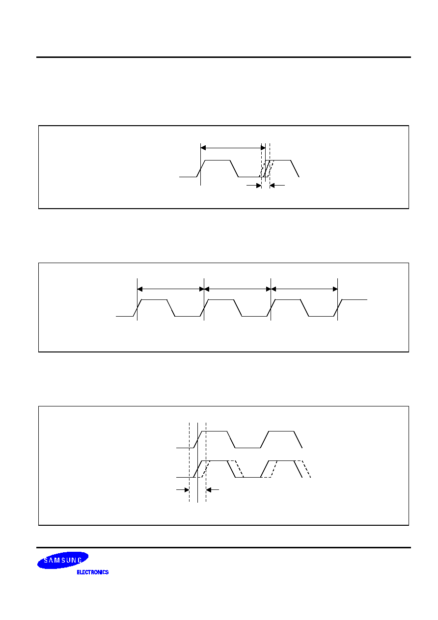
Period Jitter
Period jitter is the maximum deviation of output clock's transition from its ideal position.
T
1
TJP
Fout
Ideal Cycle
Cycle-to-Cycle Jitter
Cycle-to-cycle jitter is the maximum deviation of output clock's transition from its corresponding position of the
previous cycle.
T
i-1
T
i
T
i+1
Fout
TJCC = max (T
i+1
- T
i
)
Long-Term Jitter
Long-term jitter is the maximum deviation of output clock' transition from its ideal position, after many cycles. The
term "many" depends on the application and the frequency.
TJLP
Cycle 0
Cycle N
BW2017X
0.35
µ
µ
µ
µ
m 3MHZ-25MHZ FSPLL
16
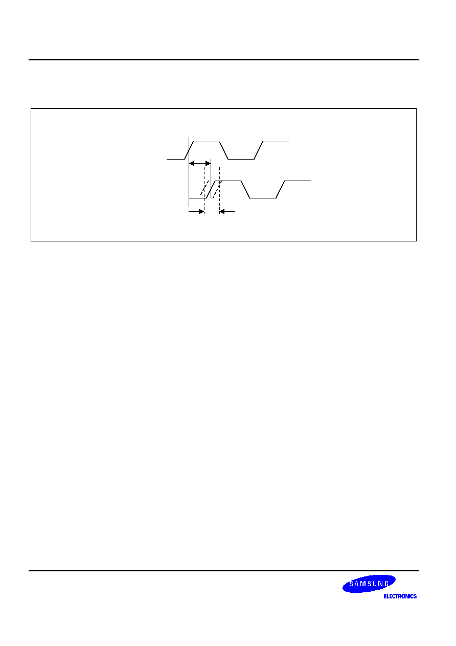
Tracking Jitter
Tracking jitter is the maximum deviation of output clock(FOUT)'s transition from input clock (FIN) position.
TJT
Delay
Fin
Trigger
Fout