 | –≠–ª–µ–∫—Ç—Ä–æ–Ω–Ω—ã–π –∫–æ–º–ø–æ–Ω–µ–Ω—Ç: BW4104X | –°–∫–∞—á–∞—Ç—å:  PDF PDF  ZIP ZIP |

0.35
µ
µ
µ
µ
m LVDS RECEIVER
BW4104X
1
GENERAL DESCRIPTION
The BW4104X receiver converts the LVDS data streams back into 28bits of CMOS/TTL data. At a transmit clock
frequency of 65MHz, 24 bits of RGB data and 4bits of LCD timing data and control data are transmitted at a rate of
455Mbps per LVDS data channel. Using a 65MHz clock the throughput is 227Mbytes/sec. Devices are offered with
falling edge clocks for convenient interface with a varity of graphics and LCD panel controllers. This receiver is an
ideal means to solve EMI and cable size problems associated with wide high speed TTL interfaces.
FEATURES
∑
20 to 65MHz shift clock support
∑
28:4 Data Channel Compression at up to 455Megabits/sec on each LVDS channel
∑
Single 3.3V supply
∑
Low Power CMOS Design
∑
Power-down mode
∑
Single pixel per clock XGA(1024x768) ready
∑
Supports VGA,SVGA,XGA and higher addressability
∑
Up to 227 Megabytes/sec bandwidth
∑
Narrow bus reduces cable size and cost
∑
PLL requires no external components
∑
Low profile 56 lead TSSOP package
∑
Falling edge data strobe Receiver

BW4104X
0.35
µ
µ
µ
µ
m LVDS RECEIVER
2
FUNCTIONAL BLOCK DIAGRAM
For channel A
For channel B
For channel C
For channel D
PLL
outbuffer x 7
outbuffer x 7
outbuffer x 7
outbuffer x 7
LVDS input buffer
Serial/Parallel
Data transfer
RAN
RAP
RBN
RBP
RCN
RCP
RDN
RDP
RCLKN
RCLKP
PDWNN
CLKOUT
RXOUT<0:6>
RXOUT<7:13>
RXOUT<14:20>
RXOUT<21:27>
Figure
1.
LVDS Block Diagram

0.35
µ
µ
µ
µ
m LVDS RECEIVER
BW4104X
3
ABSOLUTE
MAXIMUM
RATINGS
Supply
Voltage
(Vcc)
-0.3V
to
+4V
CMOS/TTL
Input
Voltage
-0.3V
to
(Vcc+0.3V)
CMOS/TTL
output
Voltage
-0.3V
to
(Vcc+0.3V)
LVDS
Receiver
Input
Voltage
-0.3V
to
(Vcc+0.3V)
Storage
Temperature
-45
∞C
to
125
∞C
NOTE: "Absolute Maximum Ratings" are thise values beyond which the safety of the device cannot guaranteed.
They are not to imply that the device should be operated at these limits. The tables of "Electrical Characteristics"
specify conditions for device operation.
RECOMMENDED
OPERATING
CONDITIONS
Parameter
Min
Typ
Max
Units
Supply
Voltage
(Vcc)
3.0
3.3
3.6
V
Operating
Temperature
-10
25
70
Receiver
Input
Range
0
2.4
V
ELECTRICAL
CHARACTERISTICS
Symbol
Parameter
Conditions
Min
Typ
Max
Units
CMOS/TTL
DC
SPECIFICATIONS
V
IH
High
Level
Input
Voltage
2
Vcc
V
V
IL
Low
Level
Input
Voltage
GND
0.8
V
V
OH
High
Level
Output
Voltage
IOH=-4mA
2.4
V
V
OL
Low
Level
Output
Voltage
IOL=4mA
0.4
V
I
IN
Input
Current
0V
VIN
VCC
± 10
mA
I
OS
Output
Short
Circuit
Current
VOUT=0V
-50
mA
LVDS
DC
SPECIFICATIONS
V
TH
Differential
Input
High
Threshold
VOM=1.2V
+100
mV
V
TL
Differential
Input
Low
Threshold
-100
mV
I
IN
Input
Current
VIN=+2.4V/0V
VCC=3.6V
± 10
mA
I
RCC
Dynamic
Current
CL=8pF,
f=65MHz
16
Gray
Scale
34
43
mA
I
RCCS
Power
Down
Current
PDWNN=Low
10
mA
BW4104X
0.35
µ
µ
µ
µ
m LVDS RECEIVER
4
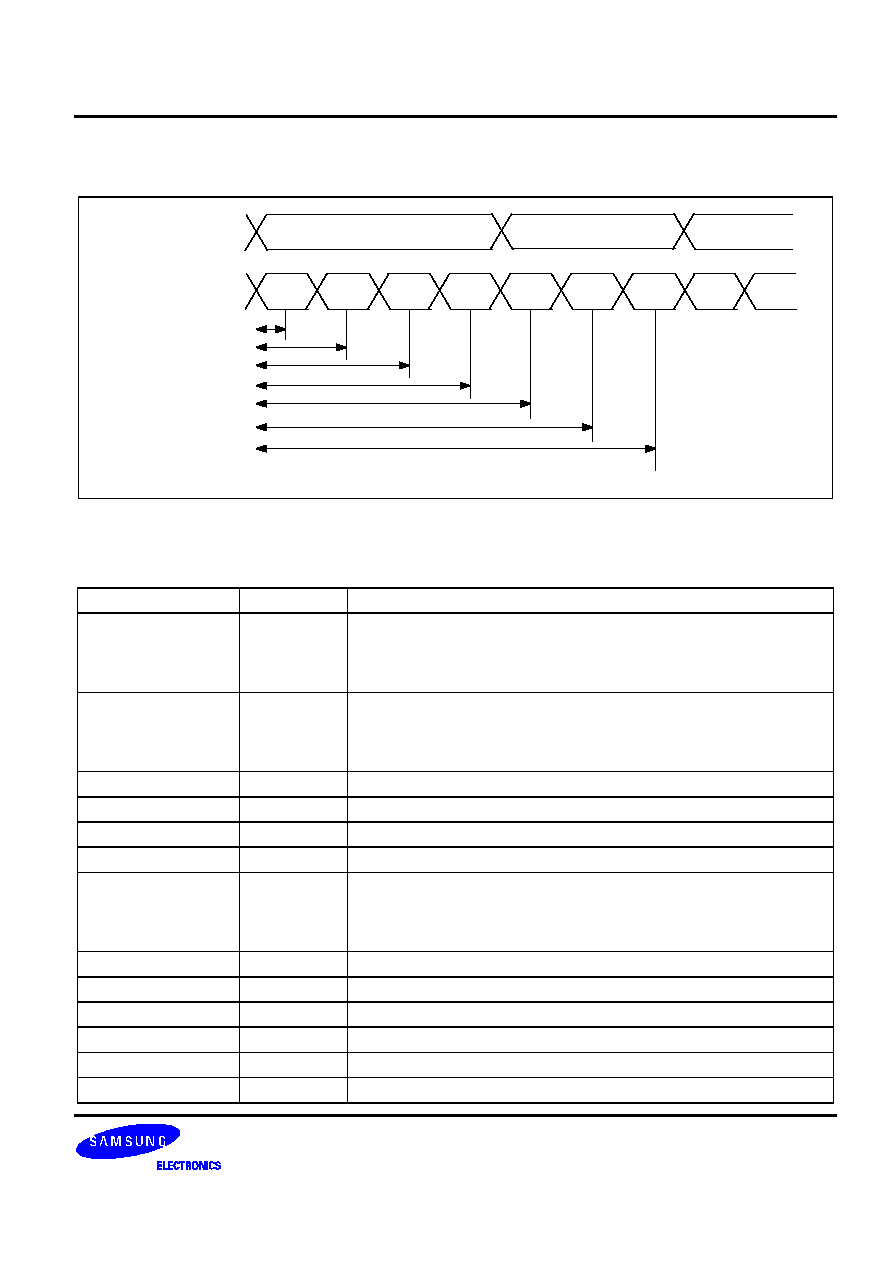
SWITCHING
CHARACTERISTICS
Symbol
Parameter
Min
Typ
Max
Units
t
RCP
CLKOUT Period
15.4
T
50
ns
t
RCH
CLKOUT High Time
4T/7
ns
t
RCL
CLKOUT Low Time
3T/7
ns
t
RS
TTL Data Setup to CLKOUT
F=65MHz
2.5
ns
t
RH
TTL Data Hold from CLKOUT
F=65MHz
4.0
ns
t
RCD
RCLKP/- to CLKOUT Delay
4T/7
ns
t
TLH
TTL Low to High Transition Time
3
5
ns
t
THL
TTL High to Low Transition Time
2
5
ns
t
RSK
LVDS Channel to Channel Skew
500
ps
t
RPLL
Phase Lock Loop Lock Time
5.2
ms

0.35
µ
µ
µ
µ
m LVDS RECEIVER
BW4104X
5
AC
TIMING
DIAGRAMS
2.0V
tRH
tRS
tRCL
tRCH
tRCD
Vdiff=0V
tRCP
2.0V
2.0V
0.8V
0.8V
CLKOUT
RCLKP/N
RAP/N
RBP/N
RCP/N
RDP/N
0.8V
0.8V
2.0V
DATA VALID
RXOUT0-RXOUT6
DATA VALID
RXOUT7-RXOUT13
DATA VALID
RXOUT14-RXOUT20
DATA VALID
RXOUT21-RXOUT27
RC6
RC5
RC4
RC3
RC2
RC1
RC0
RA6
RA5
RA4
RA3
RA2
RA1
RA0
RB6
RB5
RB4
RB3
RB2
RB1
RB0
RD6
RD5
RD4
RD3
RD2
RD1
RD0
tRSK
0.8V
2.0V
NOTE: tRSK measured between eariest and latest initial LVDS edges.
Vdiff = (RAP)-(RAN),(RBP)-(RBN),(RCP)-(RCN),(RDP)-(RDN),(RCLKP)-(RCLKN)

BW4104X
0.35
µ
µ
µ
µ
m LVDS RECEIVER
6
LVDS
INPUT
SETUP/HOLD
TIME
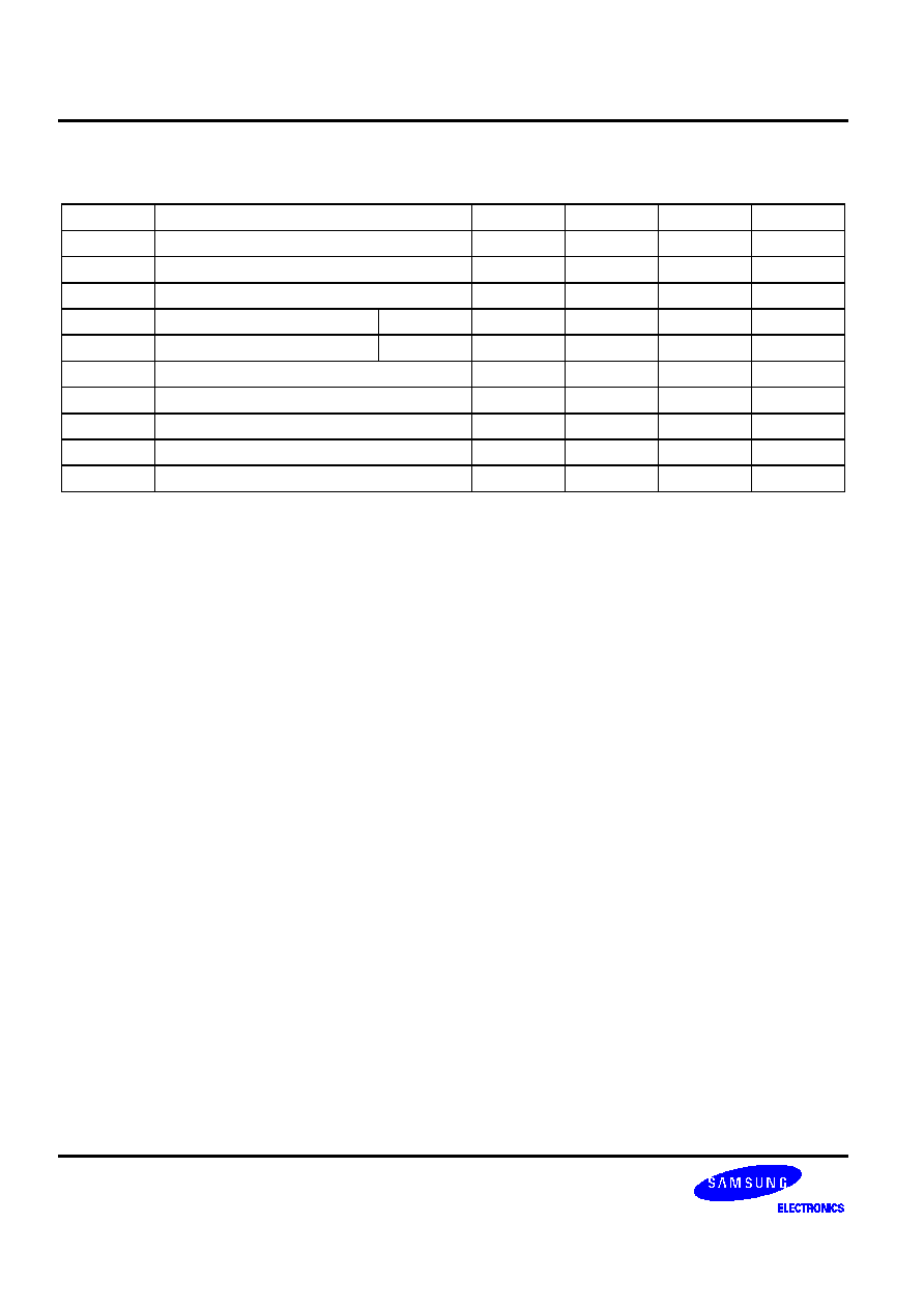
The skew margin is represented by setup time and hold time. Setup time and hold time are defined in below timing
diagram. Setup time represents "+skew" margin and hold time represents "-skew" margin. Ideal strobe position is
virtual strobe.
Note : Vdiff=(RAP-RAN,RBP-RBN,RCP-RCN,RDP-RDN)
+Skew
setup
hold
-Skew
Ideal strobe position
RAP,RBP,RCP,RDP
RAN,RBN,RCN,RDN
RAP,RBP,RCP,RDP
RAN,RBN,RCN,RDN
RAP,RBP,RCP,RDP
RAN,RBN,RCN,RDN
unit: ps
Frequency
"1" data
"0" data
setup
hold
setup
hold
65MHz
130
-80
70
-90
32MHz
140
-160
190
-150
0.35
µ
µ
µ
µ
m LVDS RECEIVER
BW4104X
7
IDEAL
STROBE
POSITION
FOR
LVDS
INPUT
Rx1
Rx0
Rx6
Rx5
Rx4
Rx3
Rx2
0.5/7T
1.5/7T
2.5/7T
3.5/7T
4.5/7T
5.5/7T
6.5/7T
RCLKP
RCLKN
RAP or RAN..etc
RAN or RAP..etc
Note: LVDS Input(RAP/RAN,RBP/RBN..etc) is 7bit data stream
PIN
DESCRIPTIONS
&
CONFIGURATIONS
Pin Name
I/O
Description
RAP
RBP
RCP
RDP
I
Positive LVDS differential data inputs
RAN
RBN
RCN
RDN
I
Negative LVDS differential data inputs
RCLKP
I
Positive LVDS differential clock inputs
RCLKN
I
Negative LVDS differential clock input
PDWNN
I
Power down signal. Active Low
CLKOUT
O
TTL level clock output. The falling edge acts as data strobe.
RXOUT<0:6>
RXOUT<7:13>
RXOUT<14:20>
RXOUT<21:27>
O
TTL level data outputs. This include 8 Red, 8 Green, 8 Blue and 4
control lines.
V
CC
P
Power supply pins for TTL outputs
GND
G
Ground pins for TTL outputs
PLL V
CC
P
Power supply for PLL
PLL GND
G
Ground pin for PLL
LVDS V
CC
P
Power Supply pin for LVDS inputs
LVDS GND
G
Ground pins for LVDS inputs

BW4104X
0.35
µ
µ
µ
µ
m LVDS RECEIVER
8
PIN
DESCRIPTIONS
&
CONFIGURATIONS (CONTINUED)
Configuration
56
55
54
53
52
51
504
9
48
47
46
45
44
43
42
41
40
39
38
37
36
35
34
33
32
31
30
29
1
2
3
4
5
6
7
8
9
10
11
12
13
14
15
16
17
18
19
20
21
22
23
24
25
26
27
28
RXOUT22
RXOUT23
RXOUT24
GND
RXOUT25
RXOUT26
RXOUT27
LVDS GND
RAN
RAP
RBN
RBP
LVDS Vcc
LVDS GND
RCN
RCP
RCLKN
RCLKP
RDN
RDP
LVDS GND
PLL GND
PLL Vcc
PLL GND
PDWNN
CLKOUT
RXOUT0
GND
Vcc
RXOUT21
RXOUT20
RXOUT19
GND
RXOUT18
RXOUT17
RXOUT16
Vcc
RXOUT15
RXOUT14
RXOUT13
GND
RXOUT12
RXOUT11
RXOUT10
Vcc
RXOUT9
RXOUT8
RXOUT7
GND
RXOUT6
RXOUT5
RXOUT4
RXOUT3
Vcc
RXOUT2
RXOUT1

0.35
µ
µ
µ
µ
m LVDS RECEIVER
BW4104X
9
TEST
METHOD
Following figures are LVDS receiver test methods. Low frequency test case is shown in Figure 1 and high
frequency test case is shown in Figure 2. For exampl, in low frequency test case LVDS input
data(RAP/N,RBP/N,etc) are input to receiver chip(Rx chip) at 65MHz, and Rx chip outputs(RXOUT<0:6>,etc) at
20MHz.
RAP
RAN
RBP
RBN
RCP
RCN
RDP
RDN
RCLKP
RCLKN
PDWNN
BW4104X
65MHz
input
20MHz
input
20MHz
output
RXOUT<0:6>
RXOUT<7:1
3>
RXOUT<14:2
0>
RXOUT<21:2
7>
CLKOUT
7
7
7
7
7
Figure 1. Low Frequency Test Case

BW4104X
0.35
µ
µ
µ
µ
m LVDS RECEIVER
10
In high frequency test case, Transmitter chip(Tx Chip) is needed. For example, Test data input to Tx chip at
65MHz,Rx chip is received LVDS data at 455MHz each channels. Test data and expectation value using this test
are made from slow frequency test result
65MHz
output
65MHz
input
RAP
RAN
RBP
RBN
RCP
RCN
RDP
RDN
RCLKP
RCLKN
BW4104X
Tx Chip
RXOUT<0:6>
RXOUT<7:13>
RXOUT<14:20>
RXOUT<21:2
7>
CLKOUT
7
7
7
7
7
7
7
7
7
7
TA<0:6>
TB<0:6>
TC<0:6>
TD<0:6>
CLKIN
PDWNN
Figure 2. High Frequency Test Case
0.35
µ
µ
µ
µ
m LVDS RECEIVER
BW4104X
11
FEEDBACK REQUEST
Thank you for having an interest in our products. Please fill out this form, especially the items which you want to
request.
Parameter
Customer
SEC
Unit
Process
Supply voltage (VDD)
Input frequency (FIN)
Output frequency (FOUT)
Cycle to cycle jitter (TJCC)
100M ~ 200M
200M ~ 300M
300M ~ 400M
400M ~ 500M
Period jitter (TJP)
100M ~ 200M
200M ~ 300M
300M ~ 400M
400M ~ 500M
Output duty ratio (TOD)
Lock up time (TLT)
Dynamic current
Stand by current
Filter capacitor
-- How many PLLs are embedded in your system ?
-- Do you need synchronization between input clock and output clock ?
-- Do you need another spec of jitter ?
Parameter
Customer
Unit
Long-term jitter (TJLT)
psec (pk-pk)
Tracking Jitter (TJT)
psec (pk-pk)
If you have another special request, please describe below.

BW4104X
0.35
µ
µ
µ
µ
m LVDS RECEIVER
12
JITTER DEFINITION
Period Jitter
Period jitter is the maximum deviation of output clock's transition from its ideal position.
T
1
TJP
Fout
Ideal Cycle
Cycle-to-Cycle Jitter
Cycle-to-cycle jitter is the maximum deviation of output clock's transition from its corresponding position of the
previous cycle.
T
i-1
T
i
T
i+1
Fout
TJCC = max (T
i+1
- T
i
)
Long-Term Jitter
Long-term jitter is the maximum deviation of output clock' transition from its ideal position, after many cycles. The
term "many" depends on the application and the frequency.
TJLP
Cycle 0
Cycle N

0.35
µ
µ
µ
µ
m LVDS RECEIVER
BW4104X
13
Tracking Jitter
Tracking jitter is the maximum deviation of output clock(FOUT)'s transition from input clock (FIN) position.
TJT
Delay
Fin
Trigger
Fout

BW4104X
0.35
µ
µ
µ
µ
m LVDS RECEIVER
14
NOTES