 | –≠–ª–µ–∫—Ç—Ä–æ–Ω–Ω—ã–π –∫–æ–º–ø–æ–Ω–µ–Ω—Ç: dac1243x | –°–∫–∞—á–∞—Ç—å:  PDF PDF  ZIP ZIP |

DAC1243X
0.25
µ
µ
m 10-BIT 300MSPS TRIPLE DAC
1
GENERAL DESCRIPTION
This core dac1243x is a triple high speed, digital-to-analog converter. It consists of three high speed, 10-bit,
video D/A converter. Its maximum conversion rate is 300MHz.
FEATURES
--
300MSPS Throughput
--
Tripe 10-Bit D/A Converters
--
SFDR
64dB at Fclk= 300Mhz; Fout=1Mhz
56dB at Fclk= 300Mhz; Fout=6Mhz
--
+2.5V power supply
--
Optional 7.5IRE(40mV) selection
--
Compatible with RS-343A output level
--
10bit Voltage parallel Input
--
Guaranteed monotonic to 10bit
--
Commercial temperature range
TYPICAL APPLICATIONS
--
Image Processing
--
High Resolution color graphic.
--
Digital TV

0.25
µ
µ
m 10-BIT 300MSPS TRIPLE DAC
DAC1243X
2
FUNCTIONAL BLOCK DIAGRAM
CCOMP
VREFOUT
IRSET
IOR
digital
decode
binary
LSBs
segmented
MSBs
DR[9:0]
5
5
7.5IRE generator
DG[9:0]
IOG
digital
decode
binary
LSBs
segmented
MSBs
5
5
7.5IRE generator
DB[9:0]
IOB
digital
decode
binary
LSBs
segmented
MSBs
5
5
7.5IRE generator
BLANKEN
VSETUP
7.5IRE
control
CLK
SLEEP
1
1
1
Reference
Block
SENSEZ
Ver 1.9 (Apr. 2002)
No responsibility is assumed by SEC for its use nor for any infringements of patents or other rights of third parties that
may result from its use. The content of this data sheet is subject to change without any notice.

DAC1243X
0.25
µ
µ
m 10-BIT 300MSPS TRIPLE DAC
3
CORE PIN DESCRIPTION
Name
I/O Type
I/O Pad
Pin Description
IOR,IOG,IOB
AO
poa_abb
Red , Greed , Blue current outputs. these high impedance
current source are capable of directly driving a double
terminated 75 W coaxial cable.
DR<9>~DR<0>
DI
picc_abb
Red, green, blue data input. These data is latched on the rising
edge of CLK. Unused data inputs should be connected to
either the regular PCB power or ground plane.
DG<9>~DG<0>
DI
picc_abb
Video signal GREEN Digital input
DB<9>~DB<0>
DI
picc_abb
Video signal BLUE Digital input
CLK
DI
picc_abb
The rising edge of CLK latches the R<9:0>,DG<9:0>,DB<9:0>
and control signal. It is typically the pixel clock rate of the
video system.
SLEEP
DI
picc_abb
Power Save Control Pin. (high active)
VREFOUT
AB
poa_bb
Voltage Reference Input for DACs or voltage reference.
External DC Voltage(0.7V) .
CCOMP
AB
poa_bb
Compensation pin. This is a compensation pin of the internal
reference amplifier. A 0.1uF ceramic capacitor must be
connected between COMP and AVDD25A.
SENSEZ
AO
poar50_bb
This pin should be connect to AVDD25A.
IRSET
AB
poa_bb
A resistor (Rset) connected between this pin and GND,
controls the magnitude of the full-scale video signal. external
resistor connection Rset(W)= Vrefout / I(IOR or IOG or IOB)
◊
31.96
VSETUP
DI
picc_abb
7.5 IRE level enable (40mV)
BLANKEN
DI
picc_abb
blank level enable
VDD25A
DP
vdd2t_abb
Digital Power (2.5V
±
5%)
VSS25A
DG
vdd2t_abb
Digital Ground
VDD25A1
AP
vss2t_abb
Analog Power supply (2.5V
±
5%)
VSS25A1
AG
vss2t_abb
Analog Ground
I/O TYPE ABBR.
-- AI: Analog Input
-- DI: Digital Input
-- AO: Analog Output
-- DO: Digital Output
-- AB: Analog Bidirectional
-- DB: Digital Bidirectional
-- AP: Analog Power
-- DP: Digital Power
-- AG: Analog Ground
-- DG: Digital Ground

0.25
µ
µ
m 10-BIT 300MSPS TRIPLE DAC
DAC1243X
4
CORE CONFIGURATION
VREFOUT
IOR
IOG
IOB
IRESET
SENSEZ
CCOMP
CLK
SLEEP
VSETUP
BLANKEN
DB[9:0]
DG[9:0]
VSS25A1
VDD25A1
VDD25A
VSS25A
VBBA
VBBA1
DR[9:0]
dac1243x

DAC1243X
0.25
µ
µ
m 10-BIT 300MSPS TRIPLE DAC
5
FUNCTIONAL DESCRIPTION
This is 10bit 300MSPS digital to analog data converter and uses segment architecture for 4bits of MSB sides ,
binary-weighted architecture for 4bits of LSB side and master slave architecture for 2bit of LSB. it contains of
First latch block, decoder block Second latch block, AMP block ,BGR block, switch buffer block, SLEEP block for
power down, CM(current mirror)block and analog switch block. This core uses reference current to decide the
1LSB current size by dividing the reference current by 32times. So the reference current must be constant and
the switch's physical real size can be constant by using OPA block with high DC gain. The most significant block
of this core is analog switch block and it must maintain the uniformity at each switch, so layout designer must
care of the matching characteristics on analog switch and CM block. And more than 80% of supply current is
dissipated at analog switch block and AMP block. And it uses samsung (SEC) standard cell as all digital cell of
latch ,decoder and buffer. And to adjust full current output, you must decide the "Rset" resistor value(connected
to IREF pin) and "Vbias" voltage value(connected to VREFOUT pin). Its voltage output can be obtained by
connecting RL1(connected to IOR,IOG,IOB pin).
Error: Linearity error is defined as the maximum deviation of the actual analog output from the ideal output, determined
by a straight line drawn from zero to full scale.
Monotonicity: A D/A converter is monotonic if the output either increases or remains constants as the digital input
increases.
Offset Error: The deviation of the output current from the ideal of zero is called offset error. For IO, 0mV output expected
when the inputs are all 0s.
Gain Errors: The difference between the actual and ideal output span. The actual span is determined by the output
when all inputs are set to 1s minus the output when all inputs are set to 0s.
Output Compliance Range: The range of allowable voltage at the output of a current-output DAC.
Operation beyond the maximum compliance limits may cause either output stage saturation or breakdown resulting in
nonlinear performance.
Settling Time: The time required for the output to reach and remain within a specified error band about its final value,
measured from the start of the output transition
Glitch Impulse : Asymmetrical switching times in a DAC give rise to undesired output transients that are quantified by a
glitch impulse. It is specified as the net area of the glitch in pV-s

0.25
µ
µ
m 10-BIT 300MSPS TRIPLE DAC
DAC1243X
6
ABSOLUTE MAXIMUM RATINGS
Characteristics
Symbol
Values
Unit
Supply Voltage
VDD25A
VDD25A1
-0.5 TO 3.3
V
Voltage on any Digital Voltage
Vin
VSS25A-0.3 to VDD25A+0.3
V
Storage Temperature Range
Tstg
-45 to 150
∞
C
NOTES:
1. It is strongly recommended that to avoid power latch-up all the supply Pins(VDD25A,VSS25A) be driven from the same
source.
2. Absolute Maximum Rating values applied individually while all other parameters are within specified operating
conditions.
Function operation under any of these conditions is not implied.
3. Applied voltage must be current limited to specified range.
4. Absolute Maximum Ratings are value beyond which the device may be damaged permanently. Normal operation is not
guaranteed.
RECOMMENDED OPERATING CONDITIONS
Characteristics
Symbol
Min
Typ
Max
Unit
Operating Supply Voltage
VDD25A
2.25
2.5
2.75
V
Digital input Voltage HIGH
LOW
Vih
Vil
0.7VDD25A
-
-
-
-
0.3VDD25A
V
Operating Temperature Range
Topr
0
25
70
∞
C
DAC1243X
0.25
µ
µ
m 10-BIT 300MSPS TRIPLE DAC
7
DC ELECTRICAL CHARACTERISTICS
Characteristics
Min
Typ
Max
Unit
Test Conditions
Resolution
Integral Linearity Error(INL)
Differential Linearity Error(DNL)
ANALOG OUTPUT
Gain Error(With external Reference)
Output Compliance Range
Output Resistance, Rout
Output Capacitance, Cout
10
-2
-2.5
-1
-
-1.0
-
1.5
1.5
0.4
±
2%
-
100K
10p
-
+2
+2.5
+1
±
10%
1.2
Bits
LSB
LSB
LSB
% of FSR
V
F
0
∞
C ~ 70
∞
C
-45
∞
C ~ 85
∞
C
Monotonicity
Guaranteed
Full Scale Current
15
-
18
mA
You can get the full
scale current by using
Rset(
)=
Vrefout/I(load)
◊
31.96
VOLTAGE REFERENCE(Ext.)
0.65
0.7
0.75
V
Power Supply Current
-
60
70
mA
NOTES:
1. Full Scale Current can be changed by using external RSET resistor
2.
Converter Specifications (unless otherwise specified)
(VDD=2.5V
±
0.25V,Vrefout=0.7V, Rset=1.27K
, Cload=10pF, Rload=37.5
)

0.25
µ
µ
m 10-BIT 300MSPS TRIPLE DAC
DAC1243X
8
AC ELECTRICAL CHARACTERISTICS
Characteristics
Symbol
Min
Typ
Max
Unit
Fclk= 100MHz; Fout =1MHz
SNDR
-
-57(R)
-56(G)
-56(B)
-
dB
Fclk= 100MHz; Fout =6MHz
SNDR
-
-52(R)
-52(G)
-53(B)
-
dB
Fclk=100MHz; Fout = 20MHz
SNDR
-
-45(R)
-46(G)
-46(B)
-
dB
Fclk= 200MHz; Fout = 1MHz
SNDR
-
-56(R)
-55(G)
-57(B)
-
dB
Fclk=200MHz; Fout = 6MHz
SNDR
-
-50(R)
-50(G)
-51(B)
-
dB
Fclk= 200MHz; Fout = 20MHz
SNDR
-
-44(R)
-45(G)
-46(B)
-
dB
Fclk= 300MHz; Fout = 1MHz
SNDR
-
-55(R)
-55(G)
-54(B)
-
dB
Fclk=300MHz; Fout = 6MHz
SNDR
-
-48(R)
-47(G)
-48(B)
-
dB
Fclk= 300MHz; Fout = 20MHz
SNDR
-
-40(R)
-46(G)
-45(B)
-
dB
NOTES:
1. Full Scale Current can be changed by using external RSET resistor.
2. Converter Specifications (unless otherwise specified) (VDD=2.5V
±
0.25V,Vrefout=0.7V,Rset=1.27K
, Cload=10pF,
Rload=37.5
, Vfs= 0.66V)
DAC1243X
0.25
µ
µ
m 10-BIT 300MSPS TRIPLE DAC
9
TIMING - SPECIFICATIONS
Characteristics
Symbol
Min
Typ
Max
Unit
Analog Output Delay
Td
-
7
9
ns
Analog Output Rise Time
Tr
-
0.5
2
ns
Analog Output Fall Time
Tf
-
0.5
2
ns
Analog Output Settling Time
Ts
-
100
120
ns
Glitch Impulse
GI
-
15
40
pVsec
Feed-through
fdth
-
44
80
dB
Data and Control Setup
Ts
-
1
-
nsec
Data and Control Hold
Th
-
1
-
nsec
Power Down On Time
-
-
5.5
-
µ
sec
Power Down Off Time
-
-
5.5
-
msec
NOTES:
1. Rising time was measured from the 10% to 90% point of zero to full-scale transition, fall time from the 90% to 10%
point
of a full scale transition.
2. Settling Time: Measured from 50% point of full-scale transition to 1% of final value.
3. Output delay measured from the 50% point of the rising edge of clock to the 50% point of full scale transition.
4. Converter Specifications (unless otherwise specified) (VDD=2.5V
±
0.25V,Vrefout=0.7V,Rset=1.27K
,
Cload=10pF,Rload=37.5
, Vfs= 0.66V)
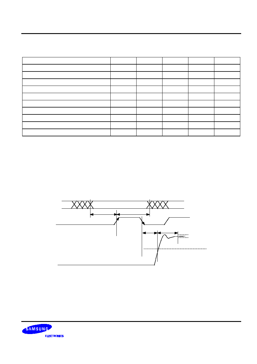
D[9:0]
IO
Ts
50%
Tset
Th
Td
0.1%
Half clock pipeline delay
CLK
Figure 1. Timing Diagram

0.25
µ
µ
m 10-BIT 300MSPS TRIPLE DAC
DAC1243X
10
TIMING DIAGRAM (FOR ONE CHANNEL)
100 IRE
BLACK LEVEL
BLANK LEVEL
WHITE LEVEL
7.5 IRE
0.714
0.54
0
7.5 IRE disable
7.5 IRE enable
mA
V
mA
V
R/G/B output
19.04
1.44
0
0.66
0
17.6
0
NOTE:
1. OUTPUT CONNECTED TO A DOUBLY TERMINATED 75
LOAD
2. Vref = 0.7V, Rset=1.27 K
Figure 2. RGB Video Output
7.5 IRE FUNCTION (FOR EACH CHANNEL)
Binary Input
DAC Output Current(Ma)
RL = 37.5 Ohm
Vsetup
Blanken
Data
Code
R,G,B Channel
0
0
000H
3FFH
0
1023
1.44
19.04
1
0
000H
3FFH
0
1023
1.44
19.04
0
1
000H
3FFH
0
1023
1.44
19.04
1
1
000H
3FFH
0
1023
0
17.6

DAC1243X
0.25
µ
µ
m 10-BIT 300MSPS TRIPLE DAC
11
CORE EVALUATION GUIDE
HOST
DSP
CORE
MUX
TEST PATH
10
10
Cc
Ct
2.5V GND
2.5V GND
Ct
0.7V
GND
RSET
(=1.27k
)
IRSETVREFOUT
DB[9:0]
IOG
VDD25A
VSS25A
VBBA
VDD25A1 VSS25A1
dac1243x
CCOMP
VBBA1
IOB
CLK
SLEEP
10
10
10
Cc
Ct
Analog
Ground
Analog
Power
Digital
Ground
Digital
Power
Analog
Ground
Analog
Power
2.5V
Cc
GND
GND
Analog
Ground
Analog
Ground
RO1
RO1
10
DG[9:0]
10
DR[9:0]
VSETUP
BLANKEN
IOR
Analog
Ground
GND
RO1
SENSEZ
2.5V
HOST
DSP
CORE
MUX
TEST PATH
10
10
Cc
Ct
2.5V GND
2.5V GND
Ct
0.7V
GND
RSET
(=1.27k
)
IRSETVREFOUT
DB[9:0]
IOG
VDD25A
VSS25A
VBBA
VDD25A1 VSS25A1
dac1243x
CCOMP
VBBA1
IOB
CLK
SLEEP
10
10
10
Cc
Ct
Analog
Ground
Analog
Power
Analog
Ground
Analog
Power
Digital
Ground
Digital
Power
Digital
Ground
Digital
Power
Analog
Ground
Analog
Power
2.5V
Cc
GND
GND
Analog
Ground
Analog
Ground
RO1
RO1
10
DG[9:0]
10
DR[9:0]
VSETUP
BLANKEN
IOR
Analog
Ground
GND
RO1
SENSEZ
2.5V
Location
Description
Cc
0.1
µ
F
R1
1.27 k
RO1
37.5
Ct
10
µ
F
Cc
0.1
µ
F

0.25
µ
µ
m 10-BIT 300MSPS TRIPLE DAC
DAC1243X
12
The voltage is scaled factor of 1/32 for VIDEO. The full scale current is given as the decimal value equivalent to
the digital code.
1. Resolution
If you want to change the resolution, use as many appear bits as you want and connect the rest lower bits to the
ground as above diagram which is 10bit application.
2. Output Range Alteration
In order to change the output swing, use following equation.
Vout = { V(IRSET)/(RSET
◊
32)}
◊
DAC_CODE
◊
Rio -(1)
Output swing level is a function of V(IRSET), RSET, and Rio, The maximum output swing level is 1.0V
3. Reference Input
A resistance Rset connected between the Rset pin and GND determines the amplitude of the output video level
according to Equations (1).

DAC1243X
0.25
µ
µ
m 10-BIT 300MSPS TRIPLE DAC
13
PHANTOM CELL INFORMATION
Pins of the core can be assigned externally (Package pins) or internally (internal ports) depending on design
methods.
The term "External" implies that the pins should be assigned externally like power pins.
The term "External/internal" implies that the applications of these pins depend on the user.
DAC1243X
10bit tripe 300MSPS DAC
V
B
B
A
V
B
B
A
V
S
E
T
U
P
B
L
A
N
K
E
N
VVSS25A
1
IOG
IRSET
IOR
CCOMP
V
D
D
2
5
A
V
S
S
2
5
A
C
L
K
VREFOUT
IOB
VREFOUT
VSS25A1
V
S
S
2
5
A
V
D
D
2
5
A
V
D
D
2
5
A
V
B
B
A
V
B
B
A
DR[7]
DR[6]
DR[5]
DR[4]
DR[3]
DR[2]
DR[1]
DR[0]
DR[9]
DR[8]
DG[7]
DG[6]
DG[5]
DG[4]
DG[3]
DG[2]
DG[1]
DG[0]
DG[9]
DG[8]
DB[7]
DB[6]
DB[5]
DB[4]
DB[3]
DB[2]
DB[1]
DB[0]
DB[9]
DB[8]
VBBA1
VBBA
VBBA1
SENSEZ
VDD25A1
VDD25A1
S
L
E
E
P

DAC1243X
0.25
µ
µ
m 10-BIT 300MSPS TRIPLE DAC
14
Pin Name
Pin Usage
Pin Layout Guide
VDD25A
External
- Maintain the large width of lines as far as the pads.
- place the port positions to minimize the length of power lines.
- Do not merge the analog powers with another power from
other blocks.
- Use good power and ground source on board.
- In Phantom cell in case of many ports of one power name,
you must drag the ports individually to PAD in parallel.
VSS25A
External
VBBA
External
VBBA1
External
VDD25A1
External
VSS25A1
External
CCOMP
External/Internal
- Do not overlap with digital lines.
- Maintain the shortest path to pads.
VREFOUT
External/Internal
IREF
External/Internal
- Separate from all other analog signals
IOR
External/Internal
- Maintain the larger width and the shorter length as far as the
pads.
- Separate from all other digital lines.
- These lines must have the same metal length because of
voltage drop through the metal line and matching
IOG
External/Internal
IOB
External/Internal
SLEEP
External/Internal
- Separated from the analog clean signals if possible.
- Do not exceed the length by 1,000um.
BLANKEN
External/Internal
VSETUP
External/Internal
DR[9:0]
External/Internal
DG[9:0]
External/Internal
DB[9:0]
External/Internal

DAC1243X
0.25
µ
µ
m 10-BIT 300MSPS TRIPLE DAC
15
PACKAGE CONFIGURATION
0.0 V
2.5V
(VSS)
(VDD)
1
2
3
4
5
6
7
8
9
10
11
12
13
14
15
16
17
18
19
20
21
22
23
24
48
47
46
45
44
43
42
41
40
39
38
37
36
35
34
33
32
31
30
29
28
27
26
25
DB6
DB5
DB4
DB3
DB2
DR9
DR8
DR7
DR6
DR5
DR4
DR3
DB7
DB8
DB9
CLK
VSS25A
VDD25A
SLEEP
VSS25A1
IOB
VREFOUT
VDD25A1
CCOMP
IOG
VDD25A1
NC
IOR
NC
SENSEZ
IRSET
VSS25A1
BS
DR0
DR1
DR2
DAC
1243X
Ct
+
Cc
GND
Analog
Ground
RO1
GND
Analog
Ground
RO1
DG9
DG8
DG7
DG6
DG5
DG4
DG3
DG2
DG1
DG0
DB1
DB0
0V or 2.5V
L1
L2
0.7V
VDD
GND
RSET
GND
RO1
VDD
Cc
BLANKEN
and VSETUP
0.0 V
2.5V
(VSS)
(VDD)
1
2
3
4
5
6
7
8
9
10
11
12
13
14
15
16
17
18
19
20
21
22
23
24
48
47
46
45
44
43
42
41
40
39
38
37
36
35
34
33
32
31
30
29
28
27
26
25
DB6
DB5
DB4
DB3
DB2
DR9
DR8
DR7
DR6
DR5
DR4
DR3
DB7
DB8
DB9
CLK
VSS25A
VDD25A
SLEEP
VSS25A1
IOB
VREFOUT
VDD25A1
CCOMP
IOG
VDD25A1
NC
IOR
NC
SENSEZ
IRSET
VSS25A1
BS
DR0
DR1
DR2
DAC
1243X
Ct
+
Cc
Cc
GND
Analog
Ground
RO1
GND
Analog
Ground
RO1
GND
Analog
Ground
RO1
DG9
DG8
DG7
DG6
DG5
DG4
DG3
DG2
DG1
DG0
DB1
DB0
0V or 2.5V
L1
L2
L1
L2
0.7V
0.7V
VDD
VDD
GND
RSET
GND
RO1
VDD
Cc
BLANKEN
and VSETUP
300MHz
Location
Description
L1,L2
Ferrite Bead ( 0.1mh )
C1
10uF Capacitor
C2
0.1uF Ceramic Capacitor
Rio
37.5 ohm Resistor
RSET
1270ohm 1% Metal Film Resistor

0.25
µ
µ
m 10-BIT 300MSPS TRIPLE DAC
DAC1243X
16
PACKAGE PIN DESCRIPTION
Pin Name
No
I/O Type
Description
DB<9:0>
-
DI
Video signal BLUE Digital input
DG<9:0>
-
DI
Video signal GREEN Digital input
DR<9:0>
-
DI
Video signal RED Digital input
VREFOUT
-
AI
Reference voltage input & monitoring
IRSET
-
AI
external resistor connection
SLEEP
-
DI
Power down mode (high active)
BLANKEN
-
DI
Blank enable pin
VSETUP
-
DI
7.5 IRE level enable
CLK
-
DI
Clock
CCOMP
-
AI
External capacitance connection
SENSEZ
-
AO
DAC output sensing
IOR
-
AO
Analog Voltage Output
IOG
-
AO
Analog Voltage Output
IOB
-
AO
Analog Voltage Output
VDD25A1
-
DP
Digital Power
VSS25A1
-
DG
Digital Ground
VBBA
-
AG
Bulk Bias Ground
VDD25A
-
AP
Analog Power
VSS25A
-
AG
Analog Ground
NOTE: I/O TYPE PP and PG denote PAD Power and PAD Ground respectively.

DAC1243X
0.25
µ
µ
m 10-BIT 300MSPS TRIPLE DAC
17
FEEDBACK REQUEST
We appreciate your interest in out products. If you have further questions, please specify in the attached form.
Thank you very much.
DC / AC Electrical Characteristic
Characteristics
Min
Typ
Max
Unit
Remarks
Supply Voltage
V
Power dissipation
mW
Resolution
Bits
Analog Output Voltage
V
Operating Temperature
∞
C
Output Load Capacitor
pF
Output Load Resistor
Ohm
Integral Non-Linearity Error
LSB
Differential Non-Linearity Error
LSB
Maximum Conversion Rate
MHz
Voltage Output DAC
Reference Voltage TOP
BOTTOM
V
Analog Output Voltage Range
V
Digital Input Format
Binary Code or 2's Complement Code
Current Output DAC
Analog Output Maximum Current
mA
Analog Output Maximum Signal
Frequency
MHz
Reference Voltage
V
External Resistor for Current
Setting(RSET)
Ohm
Pipeline Delay
sec
- Do you want to Power down mode?
- Do you want to Internal Reference Voltage(BGR)?
- Which do you want to Serial Input TYPE or parallel Input TYPE?

0.25
µ
µ
m 10-BIT 300MSPS TRIPLE DAC
DAC1243X
18
VERSION LIST
Version
Date
Modified Items
Comments
Ver 1.0
98.05.01
Original version published
Ver 1.4
99.12.13
1. Test configuration correction 2. Font correction
Ver 1.5
00.02.23
1. Layout guide correction 2. Font correction
Ver 1.6
00.11.27
1. IRSET,CCOMP pin IO type: AO
AB
Ver 1.7
01.07.14
blank_en,setup pin function modification in 7/15 page
Ver 1.8
02.04.07
Final Spec
Ver 1.9
02.04.20
Add Phantom Cell information 12page