þÿ

DAC1264X_RA3
0.18
µ
µ
m 3.3V 10-BIT 2MSPS 8-CHANNEL DAC
1
GENERAL DESCRIPTION
The dac1264x_ra3 is a CMOS 10Bit 8-channel D/A converter for general application. This digital to analog converter
has a 10bit R-string structure.
Its settling time is 500ns (Typical value).
FEATURES
-- 0.18um CMOS Process
-- Resolution : 10Bit
-- Differential Linearity Error :
±
1.0 LSB
-- Integral Linearity Error :
±
2.0 LSB
-- Analog Output Range : 0.65V 2.65V
-- Settling Time : 500ns
-- Average Power Consumption : 24.0mA
-- Power Down Mode
-- Operation Temperature Range : -40
°
C 85
°
C
-- Power Supply : 3.3V Single
1.8V (for digital input)
TYPICAL APPLICATIONS
-- CD/DVD Servo
-- Motor Control Systems
-- General Applications
0.18
µ
µ
m 3.3V 10-BIT 2MSPS 8-CHANNEL DAC
DAC1264X_RA3
2
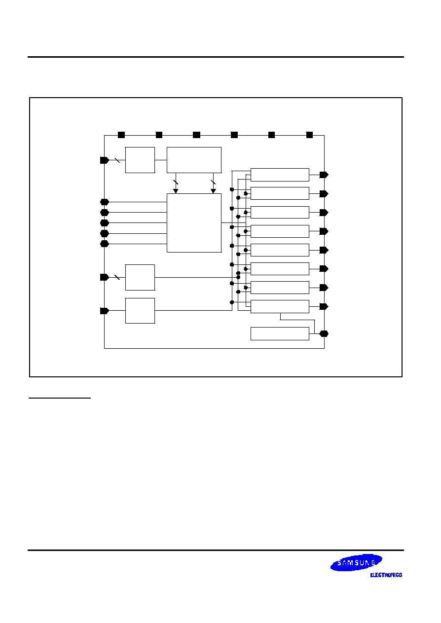
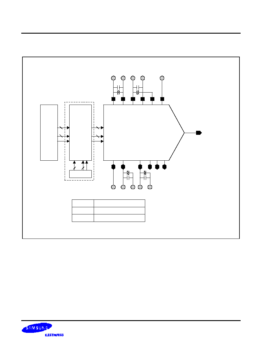
FUNCTIONAL BLOCK DIAGRAM
R-String
D[9:0]
Level
Shifter
10
Two Decoders
3.3V
2.65V
1.65V
0.65V
0.0V
VTOP
VBOT
VRT
VHALF
VRB
PWDNB
AVDD33A AVSS33A AVDD33D AVSS33D
AVBB
AVDD18D
VOUT[7]
Sample and Hold
SEL[7:0]
Level
Shifter
8
Level
Shifter
VOUT[6]
Sample and Hold
VOUT[5]
Sample and Hold
VOUT[4]
Sample and Hold
VOUT[3]
Sample and Hold
VOUT[2]
Sample and Hold
VOUT[1]
Sample and Hold
VOUT[0]
Sample and Hold
Bias Generator
NBIAS
Ver 1.3 (May 2002)
This datasheet is a preliminary version. No responsibility is assumed by SEC for its use nor for any infringements of
patents or other rights of third parties that may result from its use. The content of this datasheet is subject to change
without any notice.
DAC1264X_RA3
0.18
µ
µ
m 3.3V 10-BIT 2MSPS 8-CHANNEL DAC
3
CORE PIN DESCRIPTION
Pin Name
I/O Type
I/O Pad
Pin Description
D[9:0]
DI
picc_abb
Digital Input Data (10bit)
D[9] : MSB , D[0] : LSB
SEL[7:0]
DI
picc_abb
Channel Select Input (8bit)
SEL[7] : VOUT[7]
SEL[0] : VOUT[0]
PWDNB
DI
picc_abb
Power Down (Active Low)
VHALF
AB
phia_abb
External Voltage Reference (1.65V)
VTOP
AB
phia_abb
Voltage Reference Top (3.3V)
VBOT
AB
phia_abb
Voltage Reference Bottom (0.0V)
VRT
AB
phia_abb
Internal Voltage Reference Top (2.65V)
VRB
AB
phia_abb
Internal Voltage Reference Bottom (0.65V)
VOUT
AO
phoa_abb
Analog Voltage Output
NBIAS
AB
phia_abb
Bias Generator Output
AVDD33D
AP
vdd3t_abb
Analog Power (+3.3V)
AVSS33D
AG
vss3t_abb
Analog Ground (0.0V)
AVDD33A
DP
vdd3t_abb
Digital Power (+3.3V)
AVSS33A
DG
vss3t_abb
Digital Ground (0.0V)
AVBB
AG
vbb3t_abb
Analog Sub Bias (0.0V)
AVDD18D
DP
vdd1t_abb
Digital Power (+1.8V)
I/O Type Abbr.
-- AI: Analog Input
-- DI: Digital Input
-- AO: Analog Output
-- DO: Digital Output
-- AB: Analog Bi-direction
-- DB: Digital Bi-direction
-- AP: Analog Power
-- AG: Analog Ground
-- DP: Digital Power
-- DG: Digital Ground
0.18
µ
µ
m 3.3V 10-BIT 2MSPS 8-CHANNEL DAC
DAC1264X_RA3
4
CORE CONFIGURATION
VOUT[7:0]
VHALF
D[9:0]
SEL[7:0]
dac1264x_ra3
AVDD18D
AVBB
AVSS33A
AVDD33A
AVSS33D
AVDD33D
VTOP
VBOT
VRT
VRB
PWDNB
NBIAS
DAC1264X_RA3
0.18
µ
µ
m 3.3V 10-BIT 2MSPS 8-CHANNEL DAC
5
ABSOLUTE MAXIMUM RATINGS
Characteristic
Symbol
Value
Unit
Supply Voltage
VDD (AVDD33A,AVDD33D)
4.5
V
AVDD18D
2.5
V
Analog Output Voltage
VOUT
AVSS33A to AVDD33A
V
Digital Input Voltage
D[9:0]
AVSS33D to AVDD18D
V
Reference Voltage
VRT
VRB
AVDD33A
AVSS33A
V
Operating Temperature Range
Topr
-40 to 85
°
C
NOTES:
1. ABSOLUTE MAXIMUM RATING specifies the values beyond which the device may be damaged permanently.
Exposure to ABSOLUTE MAXIMUM RATING conditions for extended periods may affect reliability. Each condition value
is applied with the other values kept within the following operating conditions and function operation under any of these
conditions is not implied.
2. All voltages are measured with respect to VSS (AVSS33A or AVSS33D or AVBB) unless otherwise specified.
3. 100pF capacitor is discharged through a 1.5k
resistor (Human body model)
RECOMMENDED OPERATING CONDITIONS
Characteristics
Symbol
Min
Typ
Max
Unit
Supply Voltage
AVDD33A - AVSS33A
AVDD33D - AVSS33D
3.0
3.3
3.6
V
AVDD18D - AVSS33D
1.65
1.8
1.95
V
Supply Voltage Difference
AVDD33A - AVDD33D
-0.1
0.0
0.1
V
Reference Voltage
VRT
VRB
0.0
2.65
0.65
3.3
V
Digital Input 'Low' Voltage
Digital Input 'High' Voltage
VIL
VIH
0.7
×
VDD
0.3
×
VDD
V
Operating Temperature
Topr
-40
85
°
C
NOTES:
1. It is strongly recommended that to avoid power latch-up all the supply pins(AVDD33A,AVDD33D) be driven from the
same source.
2. VDD
AVDD18D
0.18
µ
µ
m 3.3V 10-BIT 2MSPS 8-CHANNEL DAC
DAC1264X_RA3
6
DC ELECTRICAL CHARACTERISTICS
(Converter Specifications: AVDD33D=AVDD33A=3.3V, AVSS33D=AVSS33A=AVBB=0V, PWDNB=High, Top=25
°
C,
VRT=2.65V, VRB=0.65V unless otherwise specified.)
Characteristics
Symbol
Min
Typ
Max
Unit
Conditions
Resolution
Bit
10
Bits
Differential Linearity Error
DLE
1.0
LSB
Integral Linearity Error
ILE
2.0
LSB
Full Scale Error
(1)
V
FS
1.998
V
VRT=2.65V , VRB=0.65V
Zero Scale Error
(1)
V
ZSE
10
mV
V
FS
= (VRT-VRB)
×
1023/1024 (ideal)
Full Scale Voltage Error
(2)
V
FSE
10
mV
= Vo
MAX
-VOUT(D[9:0]=Low) (real)
Maximum Output Voltage
Vo
MAX
2.648
V
Vo
MAX
= VOUT(D[9:0]=High)
LSB Size
V
LSB
1.953
mV
V
LSB
= (Vo
MAX
- VOUT(D[9:0]=Low))
/1023
NOTES:
1. V
ZSE
= VOUT(D[9:0] = Low) - VRB
2. V
FSE
= VOUT(D[9:0] = High) - {(VRT-VRB)
×
1023/1024 + VRB}
DAC1264X_RA3
0.18
µ
µ
m 3.3V 10-BIT 2MSPS 8-CHANNEL DAC
7
AC ELECTRICAL CHARACTERISTICS
(Converter Specifications : AVDD33D=AVDD33A=3.3V, AVSS33D=AVSS33A=AVBB=0V, load cap=25pF
load resistance=5k
, Top=25
°
C, VRT=2.65V, VRB=0.65V unless otherwise specified.)
Characteristics
Symbol
Min
Typ
Max
Unit
Conditions
Supply Current
(Average Current)
Ivdd1
24
mA
Ivdd1 = I
AVDD33A
+ I
AVDD33D
Data Input : All Low or All High
Supply Current
(Power Down Mode)
Ivdd2
10
uA
Ivdd2 = I
AVDD33A
+ I
AVDD33D
Data Rate = 2MHz
PWDNB=LOW
Reference Current
Ivrt
0.75
mA
VRT = 2.65V, VRB = 0.65V
Analog Output Delay
Td
100
ns
Data Rate = 2MHz
Data : All LOW
All HIGH
Analog Output Rise Time
Tr
110
ns
Data Rate = 2MHz
Data : All LOW
All HIGH
Analog Output Fall Time
Tf
110
ns
Data Rate = 2MHz
Data : All HIGH
All LOW
Analog Output Settling Time
Ts
500
ns
Data Rate = 2MHz
Data : All LOW
All HIGH
SEL[7:0] Pulse Width High
Tsel
250
ns
Data Rate = 2MHz
Analog Output Delay
(from SEL[7:0] to OUT[7:0])
Tseld
150
ns
Data Rate = 2MHz
Data : All LOW
All HIGH
Data Setup Time
(between D[9:0] and
SEL[7:0])
Tsels
10
ns
Data Rate = 2MHz
Data : All LOW
All HIGH
Data Hold Time
(between SEL[7:0] and
D[9:0])
Tselh
15
ns
Data Rate = 2MHz
Data : All LOW
All HIGH
Power Down On Time
Ton
100
ns
PWDNB : HIGH
LOW
Power Down Off Time
Toff
800
ns
PWDNB : LOW
HIGH
Channel Crosstalk
1
-50
dB
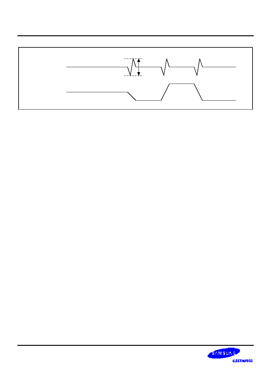
NOTE: 1. = 20log [ Vpp(max) of unselected channels/Vfs of selected channel ]
0.18
µ
µ
m 3.3V 10-BIT 2MSPS 8-CHANNEL DAC
DAC1264X_RA3
8
Unselected
Channels
Vpp
1.65V
0.65V
Selected
Channel
2.65V
0.65V
DAC1264X_RA3
0.18
µ
µ
m 3.3V 10-BIT 2MSPS 8-CHANNEL DAC
9
TIMING DIAGRAM
DATA N+1
D[9:0]
SEL[0]
SEL[1]
VOUT[0]
VOUT[1]
Tseld
DATA N-1
DATA N
Tsel
Tselh
Tsels
Tseld
DATA
Tr
PWDNB
VOUT
Ton
50%
VOUT
50%
Td
0000000000
1111111111
10%
Tf
0000000000
90%
1111111111
0000000000
DATA
VOUT
Ts
50%
0000000000
1111111111
0000000000
DATA
VOUT
0.5LSB
+
0.5LSB
+
Toff
50%
50%
0.5LSB
+
0.0V
1. SEL[7:0] fixed
2. SEL[7:0] varied
NOTES:
1. Output delay measured from the 50% point of the rising edge of input data to the full scale transition..
2. Settling time measured from the 50% point of full scale transition to the output remaining within
±
1/2 LSB.
3. Output rise/fall time measured between the 10% and 90% points of full scale transition.

0.18
µ
µ
m 3.3V 10-BIT 2MSPS 8-CHANNEL DAC
DAC1264X_RA3
10
FUNCTIONAL DESCRIPTION
1. The dac1264x_ra3 has a 10bit R-string block, two decoders, and 8 sample-and-holds.
Sample-and-hold has an OP amp, One capacitor, and a switch. The output of R-string is transmitted to selected
channel capacitor. When selected channel is disabled, sample-and-hold maintain previous voltage value. You'd
better refresh voltage values of disabled channels every 2ms for any voltage drop of internal capacitors.
2. The digital outputs of two decoders decide the voltage level of R-string block.
V
Rstring
=
2
10
VRT-VRB
9
n=0
(2
n
x D[n]) + VRB
3. The voltages of VRT and VRB are internally generated by resistor strings.
(VTOP = 3.3V , VBOT = 0.0V then VRT = 2.65V , VRB= 0.65V)
For more accurate operations, you had better connect VRT and VRB with voltage sources.
Instead of connecting VTOP and VBOT with voltage sources. (VRT = 2.65V , VRB = 0.65V)
4. The VOUT pin is dependent of digital input values.
5. The loading conditions of dac1264x_ra3 : Rload
5k
& Cload
25pF.
If Rload value is smaller than 5k
, full scale voltage may be decreased.
If Cload value is larger than 25pF, analog output may be unstable.
6. Power Down Mode reduces only analog currents (I
AVDD33A
) and reference current (I
VRT
) is always dissipated.
DAC1264X_RA3
0.18
µ
µ
m 3.3V 10-BIT 2MSPS 8-CHANNEL DAC
11
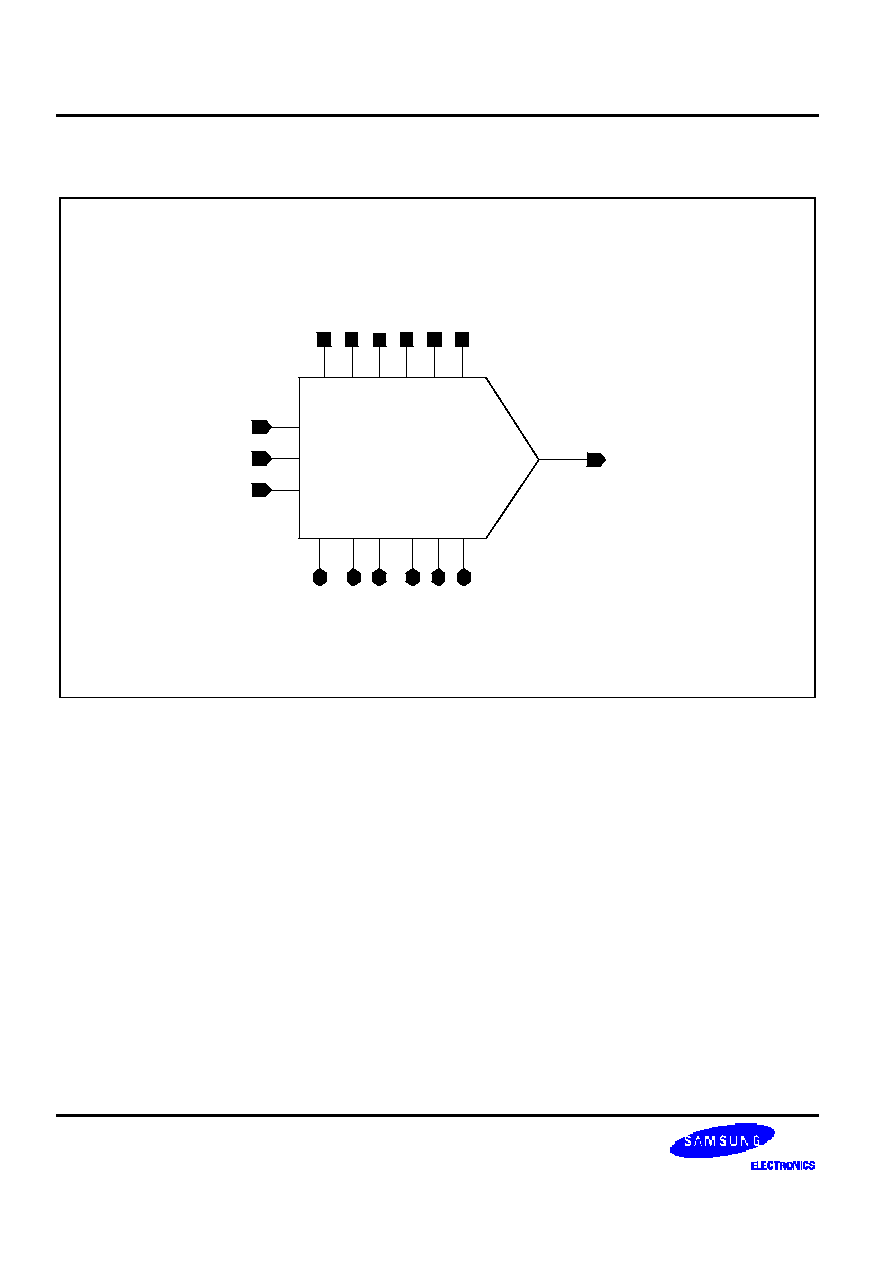
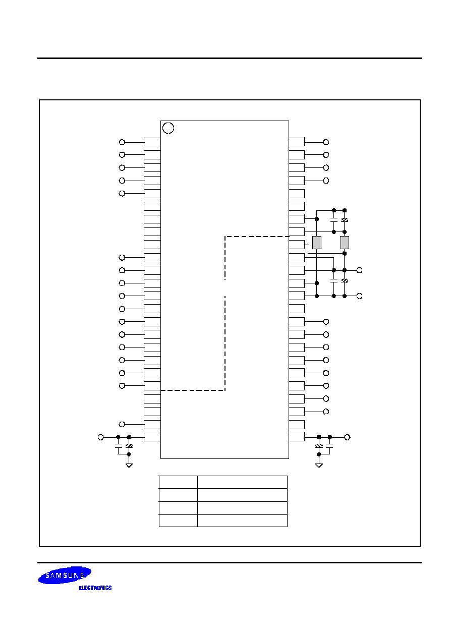
CORE EVALUATION GUIDE
VOUT[7:0]
VHALF
D[9:0]
SEL[7:0]
dac1264x_ra3
VTOP
VBOT
VRT
VRB
VOUT[7:0]
AVDD18D
AVBB
AVDD33A
AVSS33D
AVDD33D
AVSS33A
Ct
Cc
Ct
Cc
3.3V GND 3.3V GND
1.8V
1.65V 3.3V
Ct
Cc
GND 0.0V
Ct
Cc
GND
MUX
10
10
Test Path
Host
DSP
Core
10
Location
Description
Ct
10uF Tantalum Capacitor
Cc
0.1uF Ceramic Capacitor
8
8
PWDNB
8
NBIAS
TESTABLITITY
Whether you use MUX or the internal logic for testability, it is required to be able to select the values of digital inputs
( D[9:0] ).
See above figure. Only if it is, you can check the main function. (Linearity)
For more accurate operations, you had better connect VRT and VRB with voltage sources, instead of connecting
VTOP and VBOT with voltage sources. (VRT = 2.65V , VRB = 0.65V)
0.18
µ
µ
m 3.3V 10-BIT 2MSPS 8-CHANNEL DAC
DAC1264X_RA3
12
PHANTOM CELL INFORMATION
dac1264x_ra3
VOUT[7]
VOUT[6]
VOUT[5]
VOUT[4]
VOUT[3]
VOUT[2]
VOUT[1]
VOUT[0]
PWDNB
NBIAS
AVDD18D
AVBB
AVDD33A
AVSS33A
AVDD33D
AVSS33D
SEL[7:0]
VBOT
D[9:0]
VHALF
VRB
VTOP VRT
Pin Name
Property
Pin Usage
Pin Layout Guide
D[9:0]
DI
Internal/External 1. Digital Input Signal lines must have same length to reduce
SEL[7:0]
DI
Internal/External propagation delay.
PWDNB
DI
Internal/External 1. Voltage reference lines (VRT/VRB or VTOP/VBOT or
VRT
AB
External
VHALF) must be wide metal to reduce voltage drop of metal
VRB
AB
External
lines.
VTOP
AB
Internal/External 2. VOUT[7:0] signals should not be crossed by any signals and
VBOT
AB
Internal/External should not run next to digital signals to minimize capacitive
VHALF
AB
Internal/External coupling between the two signals.
VOUT[7:0]
AO
Internal/External
AVDD33A
AP
External
1. It is recommended that you use thick analog power metal.
AVSS33A
AG
External
When connected to PAD, the path should be kept as short
AVDD33D
DP
External
as possible.
AVSS33D
DG
External
2. Digital power and analog power are separately used.
AVBB
AG
External
3. Each analog power/ground (AVDD33A, AVSS33A and
AVDD18D
DP
External
AVBB) pin have two ports and you may connect just one of
them, because they are connected internally.
NOTES:
1. When the core block is connected to other blocks, it must be double guard-ring using N-well and P+ active to remove
the substrate and coupling noise.
In
that case, the power metal should be connected to PAD directly.
2. The Bulk power is used to reduce the influence of substrate noise.
DAC1264X_RA3
0.18
µ
µ
m 3.3V 10-BIT 2MSPS 8-CHANNEL DAC
13
PACKAGE CONFIGURATION
SEL[3]
AVDD18D
NC
NC
NC
NC
D[9]
D[8]
D[7]
D[6]
D[5]
D[4]
D[3]
D[2]
D[1]
D[0]
PWDN
NC
NC
NBIAS
VBOT
SEL[4]
SEL[5]
SEL[6]
SEL[7]
NC
AVDD33D
AVSS33D
AVBB
AVSS33A
AVDD33A
NC
VOUT[7]
VOUT[6]
VOUT[5]
VOUT[4]
VOUT[3]
VOUT[2]
VOUT[1]
VOUT[0]
NC
NC
VTOP
AVSS33A
AVDD33A
SEL[3]
1
2
3
4
5
6
7
8
9
10
11
12
13
14
15
16
17
18
19
20
21
22
23
24
Digital Ground
Analog Ground
SEL[2]
SEL[1]
SEL[0]
1.8V
SEL[2]
SEL[1]
SEL[0]
D[9]
D[8]
D[7]
D[6]
D[5]
D[4]
D[3]
D[2]
D[1]
D[0]
PWDNB
(0.0V in normal operation)
NBIAS
VBOT
Ct
Cc
(0.0V Typ.)
+
48
47
46
45
44
43
42
41
40
39
38
37
36
35
34
33
32
31
30
29
28
27
26
25
SEL[4]
SEL[5]
SEL[6]
SEL[7]
Ct
Cc
+
L1
L2
Ct
Cc
+
(VSS)
0.0V
3.3V
(VDD)
VTOP
Ct
Cc
(3.3V Typ.)
+
VOUT[7]
VOUT[6]
VOUT[5]
VOUT[4]
VOUT[3]
VOUT[2]
VOUT[1]
VOUT[0]
Location
Description
Ct
10uF Tantalum Capacitor
Cc
0.1uF Ceramic Capacitor
L1-L2
Ferrite Bead (0.1mh)
dac1264x_ra3
0.18
µ
µ
m 3.3V 10-BIT 2MSPS 8-CHANNEL DAC
DAC1264X_RA3
14
PACKAGE PIN DESCRIPTION
NAME
PIN NO
I/O TYPE
PIN DESCRIPTION
SEL[7:0]
1 4
45 48
DI
Channel Select (1.8V)
AVDD18D
5
DP
Digital Power (1.8V)
D[9:0]
10 19
DI
Digital Input Data (10bit , 1.8V)
PWDNB
20
DI
Power Down Mode Control (Active Low , 1.8V)
NBIAS
23
AB
Bias Generator Output (0.82V Typical)
VBOT
24
AB
External Voltage Reference Bottom (0.0V)
VTOP
25
AB
External Voltage Reference Top (3.3V)
VOUT[7:0]
27 34
AO
Analog Output (8-channel)
AVDD33A
36 , 37
AP
Analog Power (3.3V)
AVSS33A
38 , 39
AG
Analog Ground (0.0V)
AVBB
40
AG
Analog Sub Bias (0.0V)
AVSS33D
41
DG
Digital Ground (0.0V)
AVDD33D
42
DP
Digital Power (3.3V)
NC
6 9
21, 22
26, 35
43, 44
DO
No Connection
!/O TYPE ABBR.
-- AI : Analog Input
-- DI : Digital Input
-- AO : Analog Output
-- DO : Digital Output
-- AB : Analog Bidirectional
-- DB : Digital Bidirectional
-- AP : Analog Power
-- DP : Digital Power
-- AG : Analog Ground
-- DG : Digital Ground

DAC1264X_RA3
0.18
µ
µ
m 3.3V 10-BIT 2MSPS 8-CHANNEL DAC
15
PC BOARD LAYOUT CONSIDERATION
1. PC Board Considerations
To minimize noise on the power lines and the ground lines, the digital inputs need to be shielded and de-coupled.
This trace length between groups of VDD (AVDD33A, AVDD33D) and VSS (AVSS33A, AVSS33D) pins should be as
short as possible so as to minimize inductive ringing.
2. Supply De-coupling and Planes
For the de-coupling capacitor between the power line and the ground line, 0.1uF ceramic capacitor is used in parallel
with a 10uF tantalum capacitor. The digital power plane(AVDD33D) and analog power plane(AVDD33A) are
connected through a ferrite bead, and also the digital ground plane(AVSS33D) and the analog ground
plane(AVSS33A). This ferrite bead should be located within 3inches of the DAC1264X_RA3. The analog power plane
supplies power to the DAC1264X_RA3 of the analog output pin and related devices.
0.18
µ
µ
m 3.3V 10-BIT 2MSPS 8-CHANNEL DAC
DAC1264X_RA3
16
FEEDBACK REQUEST
We appreciate your interest in out products. If you have further questions, please specify in the attached form.
Thank you very much.
DC/AC Electrical Characteristic
Characteristics
Min
Typ
Max
Unit
Remarks
Supply Voltage
V
Power dissipation
mW
Resolution
Bits
Analog Output Voltage
V
Operating Temperature
°
C
Output Load Capacitor
pF
Output Load Resistor
k
Integral Non-Linearity Error
LSB
Differential Non-Linearity Error
LSB
Maximum Conversion Rate
MHz
Voltage Output DAC
Characteristics
Min
Typ
Max
Unit
Remarks
Reference Voltage TOP
BOTTOM
V
Analog Output Voltage Range
V
Digital Input Format
Binary Code or 2's Complement Code
Current Output DAC
Characteristics
Min
Typ
Max
Unit
Remarks
Analog Output Maximum Current
mA
Analog Output Maximum Signal
Frequency
kHz
Reference Voltage
V
External Resistor for Current
Setting(RSET)
k
Pipeline Delay
sec
-- Do you want to Power down mode?
-- Do you want to Internal Reference Voltage(BGR)?
-- Which do you want to serial input data type or parallel input data type?
-- Do you need 3.3V and 5V power supply in your system?
DAC1264X_RA3
0.18
µ
µ
m 3.3V 10-BIT 2MSPS 8-CHANNEL DAC
17
HISTORY CARD
Version
Date
Modified Items
Comments
Ver 1.0
01.12
Preliminary Version
Ver 1.1
02.02.19
Updated
Page 1 : Block diagram is modified, VOUT range is added
Page 2 : Pin description is added.
Page 5 : Full scale voltage is added
Page 6 : Reference current is added. Timing spec.s are modified.
Page 8 : Function description is modified.
Page 10 : Core layout guide is added.
Page 1113 : Package information is added.
Ver 1.2
02.03.19
Version Updated
Page 10 : minmize
minimize
page 14 : W
k
Ver 1.3
02.05.13
Version Updated
Page 4 : Absolute Maximum Rating is modified.
Page 8 : Functional Description is modified.
Page 10 : Diagram is modified.
Ver 1.4
03.01.23
Version Updated
Pager 11 : Diagram is modified.
Ver 1.5
03.03.06
Version Updated
Page 1 : dac1264x_ra
dac1264_ra3