 | –≠–ª–µ–∫—Ç—Ä–æ–Ω–Ω—ã–π –∫–æ–º–ø–æ–Ω–µ–Ω—Ç: dac1269x | –°–∫–∞—á–∞—Ç—å:  PDF PDF  ZIP ZIP |

DAC1269X
0.18
µ
µ
m 3.3V 12-BIT 2MSPS DAC
1
GENERAL DESCRIPTION
dac1269x is a CMOS 12Bit D/A converter for general application. This digital to analog converter has a R-string
structure.
Its settling time is 500ns (Typical value).
FEATURES
-- Resolution : 12-Bit
-- Differential Linearity Error :
±
1.0 LSB
-- Integral Linearity Error :
±
2.0 LSB
-- Settling Time : 500ns
-- Low Power Consumption : 1.5mA
-- Power Down Mode
-- Operation Temperature Range : 0
∞
C ≠ 70
∞
C
-- Power Supply : 3.3V Single
TYPICAL APPLICATIONS
-- Hard Disk Drive (HDD)
-- Battery Operated Instruments
-- Motor Control Systems
-- General Applications

0.18
µ
µ
m 3.3V 12-BIT 2MSPS DAC
DAC1269X
2
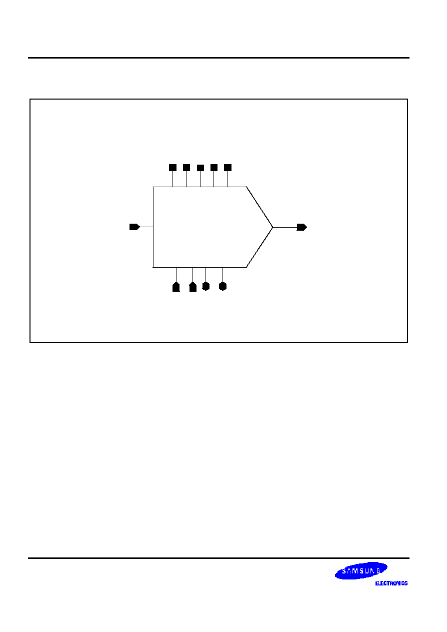
FUNCTIONAL BLOCK DIAGRAM
R-String
D[11:0]
12
N
M
Dout
Dout
2
N
2
M
REFT
REFB
+
-
3.3V
AMP
AVDD33A AVSS33A
AVDD33D AVSS33D
AVBB
VOUT
1-of-2
M
Decoder
1-of-2
N
Decoder
CNTRL
NOBUF
PWDN
SEL
SELB
PD
PWDNB
SW
SW
SEL
SELB
Ver 1.1 (Feb. 2002)
No responsibility is assumed by SEC for its use nor for any infringements of patents or other rights of third parties
that may result from its use. The content of this datasheet is subject to change without any notice.
DAC1269X
0.18
µ
µ
m 3.3V 12-BIT 2MSPS DAC
3
CORE PIN DESCRIPTION
Pin Name
I/O Type
I/O Pad
Pin Description
D[11:0]
DI
phicc_abb Digital Input Data (12bit)
D[11] : MSB , D[0] : LSB
NOBUF
DI
phicc_abb Amp Selection (High : No Amp)
PWDN
DI
phicc_abb Power Down (Active High)
REFT
AB
phoa_abb
Voltage Reference Top(max:0.9
◊
AVDD33A)
REFB
AB
phoa_abb
Voltage Reference Bottom(min:0.1
◊
AVDD33A)
VOUT
AO
phoa_abb
Analog Voltage Output
AVDD33A
AP
vdd3t_abb
Analog Power (+3.3V)
AVSS33A
AG
vdd3t_abb
Analog Ground (0.0V)
AVDD33D
DP
vdd3t_abb
Digital Power (+3.3V)
AVSS33D
DG
vss3t_abb
Digital Ground (0.0V)
AVBB
AG
vbb3_abb
Analog Sub Bias (0.0V)
I/O Type Abbr.
-- AI: Analog Input
-- DI: Digital Input
-- AO: Analog Output
-- DO: Digital Output
-- AB: Analog Bi-direction
-- DB: Digital Bi-direction
-- AP: Analog Power
-- AG: Analog Ground
-- DP: Digital Power
-- DG: Digital Ground
0.18
µ
µ
m 3.3V 12-BIT 2MSPS DAC
DAC1269X
4
CORE CONFIGURATION
VOUT
PWDN
D[11:0]
dac1269x
AVBB
AVSS33A
AVDD33A
AVSS33D
AVDD33D
NOBUF
REFT
REFB
DAC1269X
0.18
µ
µ
m 3.3V 12-BIT 2MSPS DAC
5
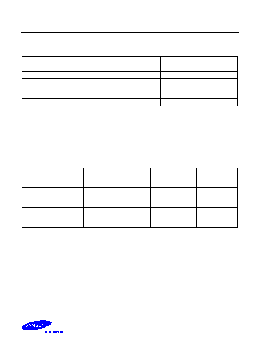
ABSOLUTE MAXIMUM RATINGS
Characteristic
Symbol
Value
Unit
Supply Voltage
VDD (AVDD33A, AVDD33D)
4.5
V
Analog Output Voltage
VOUT
VSS to VDD
V
Digital Input Voltage
D[11:0]
VSS to VDD
V
Reference Voltage
REFT
REFB
VDD
VSS
V
Operating Temperature Range
Topr
-45 to 120
∞
C
NOTES:
1. ABSOLUTE MAXIMUM RATING specifies the values beyond which the device may be damaged permanently.
Exposure to ABSOLUTE MAXIMUM RATING conditions for extended periods may affect reliability. Each condition value
is applied with the other values kept within the following operating conditions and function operation under any of these
conditions is not implied.
2. All voltages are measured with respect to VSS (AVSS33A or AVSS33D or AVBB) unless otherwise specified.
3. 100pF capacitor is discharged through a 1.5k
resistor (Human body model)
RECOMMENDED OPERATING CONDITIONS
Characteristics
Symbol
Min
Typ
Max
Unit
Supply Voltage
AVDD33A - AVSS33A
AVDD33D - AVSS33D
3.15
3.3
3.45
V
Supply Voltage Difference
AVDD33A - AVDD33D
-0.1
0.0
0.1
V
Reference Voltage
REFT
REFB
1.0
0.3
≠
≠
3.0
2.0
V
Digital Input 'Low' Voltage
Digital Input 'High' Voltage
VIL
VIH
VSS
0.7
◊
VDD
≠
≠
0.3
◊
VDD
VDD
V
Operating Temperature
Topr
0
≠
70
∞
C
NOTES:
1. Be sure that the voltage of REFT should be 1.0V larger than that of REFB at least.
2. It is strongly recommended that to avoid power latch-up all the supply pins (AVDD33A,AVDD33D) be driven from the
same source.