 | –≠–ª–µ–∫—Ç—Ä–æ–Ω–Ω—ã–π –∫–æ–º–ø–æ–Ω–µ–Ω—Ç: dac1331x | –°–∫–∞—á–∞—Ç—å:  PDF PDF  ZIP ZIP |
DAC1331X
0.18
µ
µ
m 10-BIT 40MSPS DAC
1
GENERAL DESCRIPTION
The DAC1331X core is a CMOS 10-bit dual D/A Converter Wireless Lan application. The typical conversion rate
is 40MHz. It is fabricated with 0.18um process and operated at 1.8Vsingle power.
FEATURES
-- 40MSPS operation
-- +1.8V single power supply
-- 0 ~ 0.5V output swing
-- Power down mode (active HIGH)
-- Two's complementary parallel input
TYPICAL APPLICATION
-- Wireless Lan Card
-- CDMA
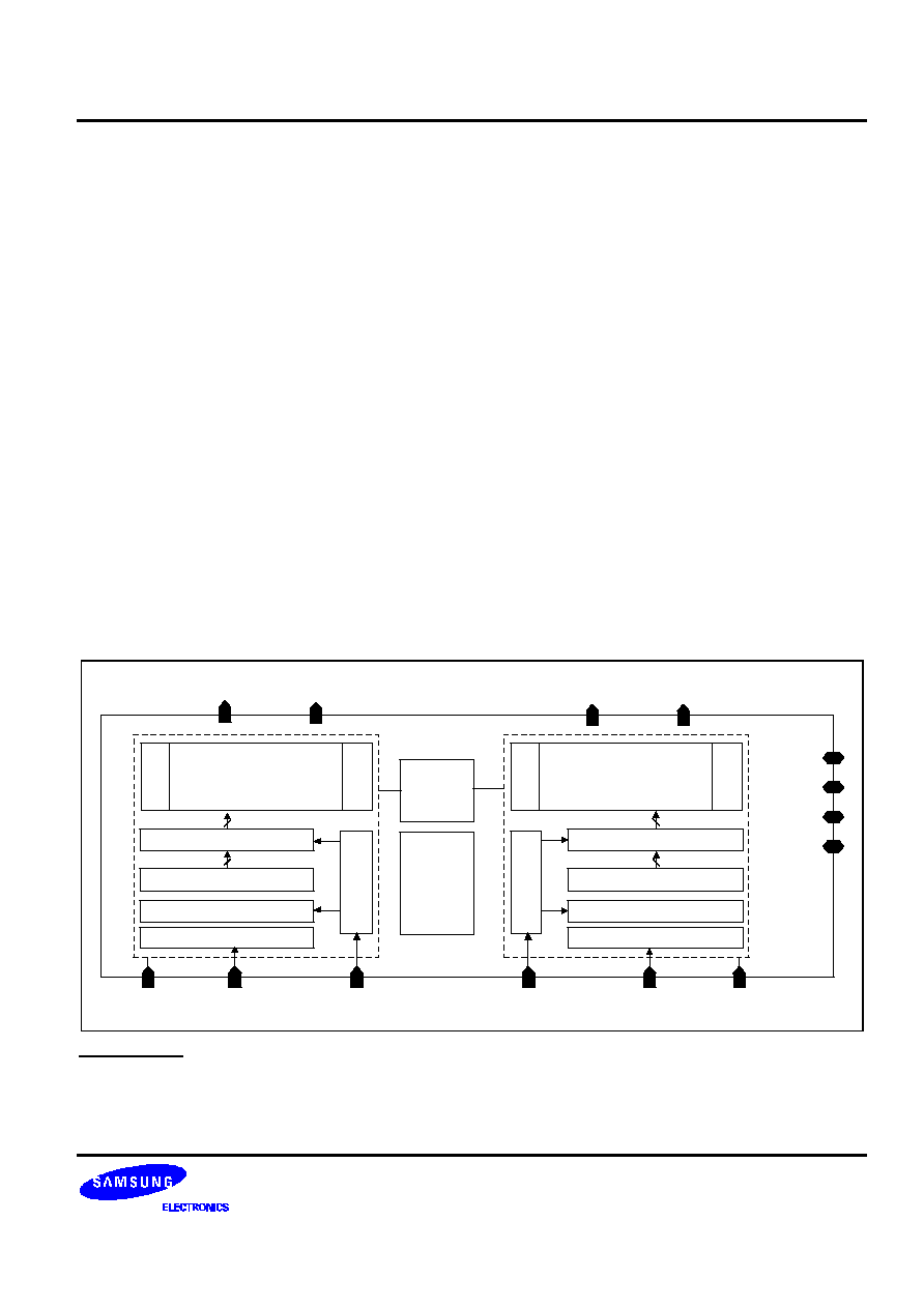
FUNCTIONAL BLOCK DIAGRAM
TXIN
TXQP
TXQN
DI[9:0]
CLKI
CLKQ
IRSET
VREFOUT
DQ[9:0]
PDQ
Decoder
IB & 1'st Latch
2'nd Latch
Analog Switch
CKGEN
Decoder
IB & 1'st Latch
2'nd Latch
Analog Switch
CKGEN
36
OPA
PDI
TXIP
Level shifter
Level shifter
CCOMP
SIN
REF
CR
CR
CR
CR
36
36
36
1.3 (Apr. 2002)
No responsibility is assumed by SEC for its use nor for any infringements of patents or other rights of third parties
that may from its use. The content of this datasheet is subject to without any notice.
0.18
µ
µ
m 10-BIT 40MSPS DAC
DAC1331X
2
CORE PIN DESCRIPTION
Pin Name
I/O Type
I/O Pad
Pin Description
TXIP,TXIN
TXQP,TXQN
AO
poa_abb
Analog Output Voltage
DI[9:0],
DQ[9:0]
DI
picc_abb
Digital Input
PDI,PDQ
DI
picc_abb
power down and standby mode
CLKI, CLKQ
DI
picc_abb
Clock Input
VREFOUT
AI
poa_abb
Bias (0.4V)
IRSET
AO
poa_abb
Probing pin
CCOMP
AB
poa_abb
Using Compensation Capacitor(0.1uF)
SIN
AB
poa_abb
Using Compensation Capacitor(0.1uF)
AVDD18A
AP
vdd1t
Analog Power
AVSS18A
AG
vss1t
Analog Ground
AVDD18D
DP
vdd1t
Digital Power
AVSS18D
DP
vss1t
Digital Ground
AVBB18A
AG
vbb1t
Analog Ground (bulk bias )
AVBB18D
AG
vbb1t
Analog Ground ( bulk bias )
I/O Type Abbr.
-- AI: Analog Input
-- DI: Digital Input
-- AO: Analog Output
-- DO: Digital Output
-- AB: Analog Bi-direction
-- DB: Digital Bi-direction
-- AP: Analog Power
-- AG: Analog Ground
-- DP: Digital Power
-- DG: Digital Ground

DAC1331X
0.18
µ
µ
m 10-BIT 40MSPS DAC
3
CORE CONFIGURATION
TXQP
DI[9:0]
dac1331x
AVBB18D
AVSS18A
AVDD18A
AVBB18A
AVSS18D
AVDD18D
DQ[9:0]
PDI
PDQ
CCOMP
SIN
IRSET
VREFOUT
CLKI
CLKQ
TXQN
TXIN
TXIP

0.18
µ
µ
m 10-BIT 40MSPS DAC
DAC1331X
4
FUNCTIONAL DESCRIPTION
This is 10bit 40MSPS dual digital to analog data converter and uses segment architecture for 5bits of MSB sides,
binary-weighted architecture for 5bits of LSB side It contains of First latch block, decoder block Second latch
block, AMP block , switch buffer block, REF block for power down, CM(current mirror)block and analog switch
block. This core uses reference current to decide the 1LSB current size by dividing the reference current by
32times. So the reference current must be constant and the switch's physical real size can be constant by using
OPA block with high DC gain. The most significant block of this core is analog switch block and it must maintain
the uniformity at each switch, so layout designer must care of the matching characteristics on analog switch and
CM block. To adjust full current output, you must force the "vrefout" voltage source value.
Error
: Linearity error is defined as the maximum deviation of the actual analog output from the ideal
output, determined by a straight line drawn from zero to full scale.
Monotonicity : A D/A converter is monotonic if the output either increases or remains constants as the digital
input increases.
Offset Error
: The deviation of the output current from the ideal of zero is called offset error. For IO, 0mV
output expected when the inputs are all 0s.
Gain Errors
: The difference between the actual andideal output span. The actual span is determined by the
output when all inputs are set to 1s minus the output when all inputs are set to 0s.
Output Compliance Range : The range of allowable voltage at the output of a current-output DAC.
Operation beyond the maximum compliance limits may cause either output stage saturation or
breakdown resulting in nonlinear performance.
Settling Time : The time required for the output to reach and remain within a specified error band about its final
value, measured from the start of the output transition
Glitch Impulse
: Asymmetrical switching times in a DAC give rise to undesired output transients that are
quantified by a glitch impulse. It is specified as the net area of the glitch in pV-s.

DAC1331X
0.18
µ
µ
m 10-BIT 40MSPS DAC
5
ABSOLUTE MAXIMUM RATINGS
Characteristic
Symbol
Values
Unit
Supply Voltage
VDD
2.5
V
Digital Input Voltage
CK
PD
VIN
AVSS18D to AVDD18D
V
Storage Temperature Range
Tstg
-45 to 150
∞
C
NOTES:
1. It is strongly recommended that to avoid power latch-up all the supply Pins(AVDD18A,AVSS18A) be driven from the
same source.
2. Absolute Maximum Rating values applied individually while all other parameters are within specified operating
conditions.
Function operation under any of these conditions is not implied.
3.
Applied voltage must be current limited to specified range.
4. Absolute Maximum Ratings are value beyond which the device may be damaged permanently. Normal operation is not
guaranteed.
RECOMMENDED OPERATING CONDITIONS
Characteristics
Symbol(Name)
Min
Typ
Max
Unit
Operating Supply Voltage
AVDD25D-AVSS25D
AVDD25A-AVSS25A
1.7
1.8
1.9
V
Reference Input
Voltage(External)
VREFOUT
≠
0.4
≠
V
Operating Temperature
Range
TOPR
-40
≠
85
∞
C
NOTE: It is strongly recommended that to avoid power latch-up all the supply pins(AVDD18A,AVDD18D)
be driven from
the same source.
0.18
µ
µ
m 10-BIT 40MSPS DAC
DAC1331X
6
DC ELECTRICAL CHARACTERISTICS
Characteristics
Symbol
Min
Typ
Max
Unit
Resolution
-
-
10
-
Bits
Differential Linearity Error
DLE
-
-
±
1
LSB
Integral Linearity Error
ILE
-
-
±
2
LSB
Monotonicity
-
-
Guaranteed
-
-
Analog Output Voltage Range
-
-
1 V
PP
0.5 V
PP
-
Differential
Single ended
Maximum Output Compliance
Voc
0
-
+ 0.6
V
External Reference Voltage
-
-
0.4
-
V
Full Scale Error (differential)
-50
-
50
mV
IQ Gain Mismatch
-0.18
0.18
dB
Power Supply Current
Is
-
25
-
mA
NOTE: Converter Specifications (unless otherwise specified)
Output Loading Condition : Output Load Capacitor = 10pF ,Output Load Resistor = 50
AC ELECTRICAL CHARACTERISTICS
Characteristics
Symbol Min
Typ
Max
Unit
Conditions
Maximum Conversion Rate
f
C
-
40
MSPS Data Rate = 1 ~ 17MHz
Dynamic Supply Current
Ivdd1
-
25
-
mA
Ivdd1 = I
AVDD18A
+ I
AVDD18D
Dynamic Supply Current
(Power Down Mode)
Ivdd2
-
50
-
uA
Ivdd2 = I
AVDD18A
+ I
VRT
+ I
AVDD18D
PDI,PDQ=HIGH
Analog Output Delay
Td
-
20
-
ns
DATA : All Low to All High
Analog Output Rise Time
Tr
-
30
-
ns
DATA : All Low to All High
Analog Output Fall Time
Tf
-
3.0
-
ns
DATA : All Low to All High
Analog Output Settling Time
Ts
-
50
-
ns
DATA : All Low to All High
Glitch Impulse
GI
-
100
-
pVsec
Feedthrough
fdth
-
90
-
dB
Setup Time
Ts
-
1
-
nsec
Hold Time
Th
-
1
-
nsec
Power Down On/Off time
-
-
500/500
-
usec
PDI/PDQ : LOW to HIGH
HIGH to LOW
SNDR( Fout=1MHz,
Fck=40MHz)
SNDR
48
-
-
dB
Fout = 1 ~ 17MHz
NOTES:
1.
The above parameters are guaranteed over the full temperature range.
2.
Clock and data feed through is a function of the amount of overshoot and undershoot on the digital inputs Settling time
does not include clock and data feed through . Glitch impulse include clock and data feed through.
3.
Setup and Hold Time are simulation values, not a test result.

DAC1331X
0.18
µ
µ
m 10-BIT 40MSPS DAC
7
TIMING DIAGRAM (FOR ONE CHANNEL)
Data
Input
TXIP,TXIN,TXQP,TXQN
Ts
50%
Tset
Th
Td
Half clock pipeline delay
CLKI,CLKQ
0.1%
NOTES:
1. Output delay measured from the 50% point of the rising edge of CLKI,CLKQ to the full scale transition.
2. Settling time measured from the 50% point of full scale transition to the output remaining within
±
1,2LSB..
3. Output rise/fall time measured between the 10% and 90% points of full scale transition.
PC BOARD LAYOUT CONSIDERATIONS
1. PC Board Considerations
To minimize Noise On The Power Lines And The Ground Lines, The Digital Inputs Need To Be Shielded And
Decoupled. This Trace Length Between Groups Of AVDD18A,AVDD18D pins short as possible so as to
minimize inductive ringing.
2. Supply Decoupling and Planes
For the de-coupling capacitor between the power line and the ground line, 0.1mFceramic capacitor is used in
parallel with a 10mF tantalum capacitor. The digital power plane (AVDD18D) and analog power plane
(AVDD18A) are connected through a ferrite bead, and also the digital ground plane (AVSS18D) and the analog
ground plane (AVSS25A). This ferrite bead should be located within 3inches of the DAC1331X. The analog power
plane supplies power to the DAC1331X of the analog output pin and related devices.
3. Analog Signal Interconnection
To minimized noise pickup and reflections due to impedance mismatch, the DAC1331X should be located as
close as possible to the output connector.
The line between DAC output and monitor input should also be regarded as a transmission line. Due to the fact,
it can cause problems in transmission line mismatch. As a solution to these problems, the double-termination
methods used. By using this, both ends of the termination lines are matched, providing an ideal, non-reflective
system.
0.18
µ
µ
m 10-BIT 40MSPS DAC
DAC1331X
8
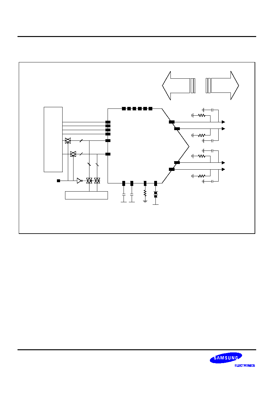
CORE EVALUATION GUIDE
DSP
BLOCK
TEST logic and mux
Test Selection
R1: 50
, R2:1270
(Load Resistance)
Cp:10pF (parasitic capacitance)
CLKI
CLKQ
TXIP
TXIN
DI[9:0]
AVDD18A
PDI
DAC1331X
BaseBand
RF
PDQ
10
DQ[9:0]
AVDD18A
AVSS18A
AVDD18D
AVSS18D
AVBB18A
AVBB18D
SIN
R1
Cp
R1
Cp
TXQN
TXQP
R1
Cp
R1
Cp
10
10
10
CCOMP
AVDD18A
0.1uF
0.1uF
IRSET
R2
VREFOUT
DC = 0.4V
NOTES:
In order to reduce the number of I/O pad, you can tie AVBB18A, AVBB18D port to AVSS18A and share the AVDD18D ,
AVSS18D with other digital power and ground. We don't offer Test logic block. So if you need test logic block, you must
make it by yourself as.
The voltage is scaled factor of 1/32 for this core. The full scale current is given as the decimal value equivalent to the digital
code.
1. Resolution
If you want to change the 10bit resolution to 8bit resolution with the same output voltage, connect the rest lower two pin
to ground.
2. Output Range Alteration
In order to change the output swing , use following equation.
Vout(TXIP,TXIN,TXQP,TXQN) = { Vrefout / (R2*M)}*(1023)*50
The maximum output swing level is 0.5V when M, R2 are 32, 2.23k
respectively.
DAC1331X
0.18
µ
µ
m 10-BIT 40MSPS DAC
9
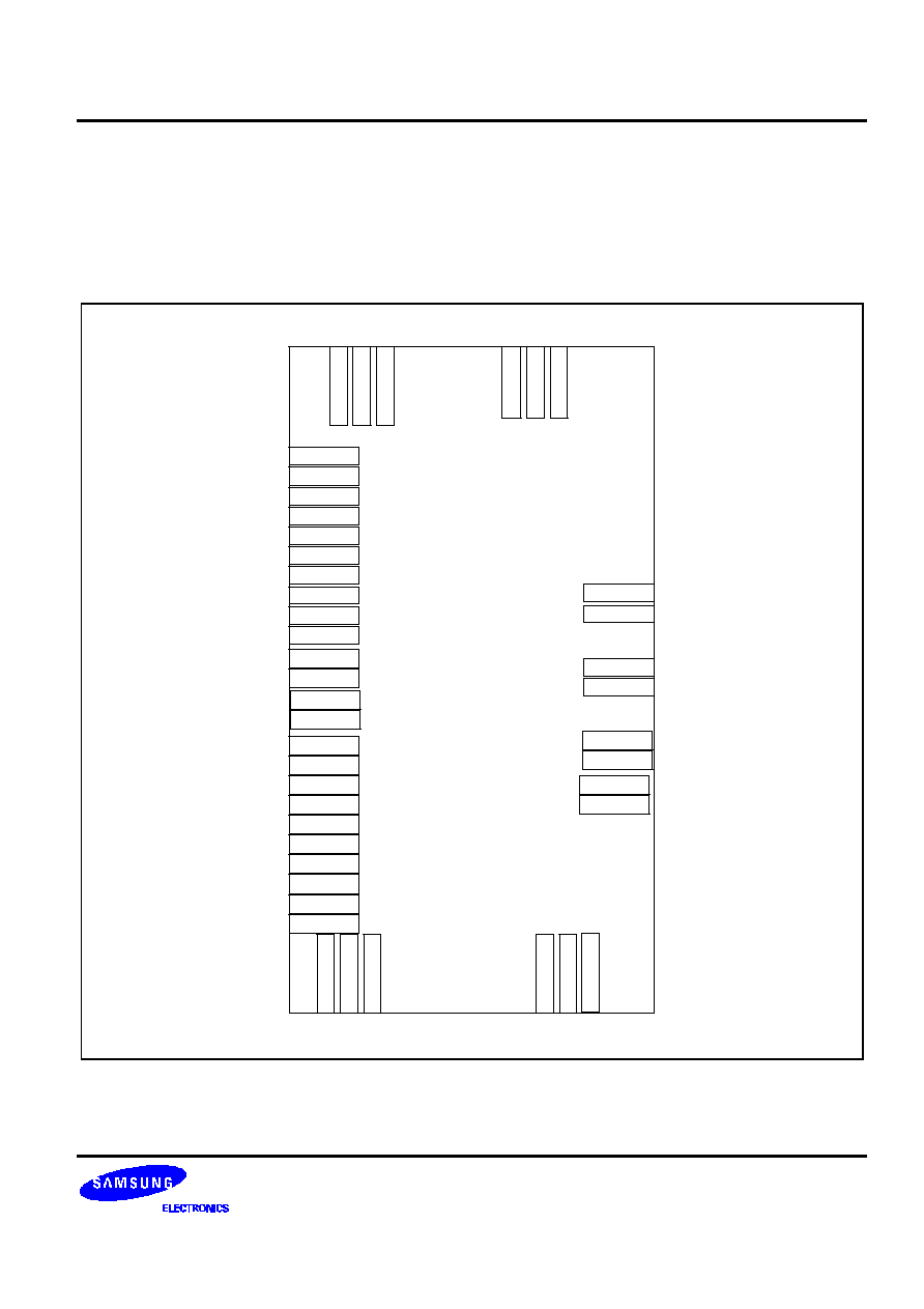
PHANTOM CELL INFORMATION
-- Pins of the core can be assigned externally (Package pins) or internally (internal ports) depending on design
methods.
The term "External" implies that the pins should be assigned externally like power pins.
The term "External/internal" implies that the applications of these pins depend on the user.
dac1331x
10bit 40MSPS DAC
A
V
D
D
1
8
A
A
V
S
S
1
8
A
A
V
B
B
1
8
A
TXIN
CCOMP
TXIP
SIN
DQ[9]
DQ[8]
DQ[7]
DQ[6]
DQ[5]
DQ[4]
DQ[3]
DQ[2]
DQ[1]
DQ[0]
A
V
B
B
1
8
A
A
V
S
S
1
8
A
A
V
D
D
1
8
A
A
V
B
B
1
8
D
A
V
S
S
1
8
D
A
V
D
D
1
8
D
A
V
B
B
1
8
D
A
V
S
S
1
8
D
A
V
D
D
1
8
D
PDI
CLKI
DI[9]
DI[8]
DI[7]
DI[6]
DI[5]
DI[4]
DI[3]
DI[2]
DI[1]
DI[0]
CLKQ
PDQ
VREFOUT
IRSET
TXIN
TXIP

0.18
µ
µ
m 10-BIT 40MSPS DAC
DAC1331X
10
Pin Name
Pin Usage
Pin Layout Guide
AVDD18A
External
- Maintain the large width of lines as far as the pads.
AVSS18A
External
- place the port positions to minimize the length of power lines.
AVBB18A
External
- Do not merge the analog powers with another power from other blocks.
AVDD18D
External
- Use good power and ground source on board.
AVSS18D
External
AVBB18D
External
CCOMP
External
- Do not overlap with digtal lines.
IRSET
External
- Maintain the shortest path to pads.
SIN
External
- Separate from all other analog signals
TXIP/TXIN
External
- Maintain the larger width and the shorter length as far as the pads.
TXQP/TXQN
External
- Separate from all other digital lines.
CLKI
External/Internal
- Separated from the analog clean signals if possible.
CLKQ
External/Internal
- Do not exceed the length by 1,000um.
DI[9]
External/Internal
- In Phantom cell in case of many ports of one power name , you must
DI[8]
External/Internal
drag the ports individually to PAD in parallel.
DI[7]
External/Internal
- Customer must use two PAD's individually for analog power ports
DI[6]
External/Internal
because of PAD's current limitation.
DI[5]
External/Internal
DI[4]
External/Internal
DI[3]
External/Internal
DI[2]
External/Internal
DI[1]
External/Internal
DI[0]
External/Internal
PDI
External/Internal
PDQ
External/Internal
DI[9]
External/Internal
DI[8]
External/Internal
D[7]
External/Internal
D[6]
External/Internal
D[5]
External/Internal
D[4]
External/Internal
D[3],D[2]
External/Internal
D[1],D[0]
External/Internal

DAC1331X
0.18
µ
µ
m 10-BIT 40MSPS DAC
11
FEEDBACK REQUEST
We appreciate your interest in our products. If you have further questions, please specify in the attached form.
Thank you very much.
DC / AC Electrical Characteristic
Characteristics
Min
Typ
Max
Unit
Remarks
Supply Voltage
V
Power dissipation
mW
Resolution
Bits
Analog Output Voltage
V
Operating Temperature
∞
C
Output Load Capacitor
pF
Output Load Resistor
Integral Non-Linearity Error
LSB
Differential Non-Linearity Error
LSB
Maximum Conversion Rate
MHz
Voltage Output DAC
Characteristics
Min
Typ
Max
Unit
Remarks
Reference Voltage TOP
BOTTOM
V
Analog Output Voltage Range
V
Digital Input Format
Binary Code or 2's Complement Code
Current Output DAC
Characteristics
Min
Typ
Max
Unit
Remarks
Analog Output Maximum Current
mA
Analog Output Maximum Signal
Frequency
kHz
Reference Voltage
V
External Resistor for Current Setting
(RSET)
Pipeline Delay
sec
-- Do you want to Power down mode?
-- Do you want to Internal Reference Voltage (BGR)?
-- Which do you want to serial input type or parallel input type?

0.18
µ
µ
m 10-BIT 40MSPS DAC
DAC1331X
12
HISTORY CARD
Version
Date
Modified Items
Comments
Ver 1.0
01.05.27
Original version published
Ver 1.1
01.08.03
VREFOUT : 0.7V
0.4V
Power Down On/Off Time addition (5/10 page)
Power Down Current (5/10 page)
Ver 1.2
02.02.28
Typo correction
Ver 1.3
02.04.20
Add Phantom cell guide