
Revision 0.3
January 2006
K1B5616BA(B)M
- 1 -
UtRAM
Preliminary
256Mb (16M x 16 bit) UtRAM
INFORMATION IN THIS DOCUMENT IS PROVIDED IN RELATION TO SAMSUNG PRODUCTS, AND
IS SUBJECT TO CHANGE WITHOUT NOTICE.
NOTHING IN THIS DOCUMENT SHALL BE CONSTRUED AS GRANTING ANY LICENSE, EXPRESS
OR IMPLIED, BY ESTOPPEL OR OTHERWISE, TO ANY INTELLECTUAL PROPERTY RIGHTS IN
SAMSUNG PRODUCTS OR TECHNOLOGY.
ALL INFORMATION IN THIS DOCUMENT IS PROVIDED ON AS "AS IS" BASIS WITHOUT GUAR-
ANTEE OR WARRANTY OF ANY KIND.
1. For updates or additional information about Samsung products, contact your nearest Samsung office.
2. Samsung products are not intended for use in life support, critical care, medical, safety equipment, or similar
applications where Product failure could result in loss of life or personal or physical harm, or any military or defense
application, or any governmental procurement to which special terms or provisions may apply.
* Samsung Electronics reserves the right to change products or specification without notice.

Revision 0.3
January 2006
K1B5616BA(B)M
- 2 -
UtRAM
Preliminary
Document Title
16Mx16 bit Synchronous Burst Uni-Transistor Random Access Memory
Revision History
Revision No. History Draft
Date
Remark
0.0
Initial
July 29, 2005
Preliminary
- Design target
0.1
Revised
September 13, 2005
Preliminary
- Added ADV interrupt comment in
Burst READ(ADV Interrupt) and Burst WRITE(ADV Interrupt).
- Changed I
CC3
latency in test conditions
from latency 3 to latency 5.
- Defined DC values
I
CC2
: 40mA
I
CC3
: 40mA
I
SB1
: 200
�A < 40�C , 350�A < 85�C.
- Errata Correction.
0.2
Revised
September 16, 2005
Preliminary
- Deleted t
ADV
, t
AS(A)
, t
AH(A)
,t
CSS(A)
in Mode 1(Async. Read
and Async. Write)
- Changed t
AS(A)
from 0ns to 5ns in Mode 2(Sync. Read
and Async. Write)
0.21
Revised
November 8, 2005
Preliminary
- Errata Correction in AC test conditions.
0.3
Revised
January 23, 2006
Preliminary
- Changed AC Parameter
tWL : 10ns 12ns
tWH : 10ns(66MHz)/ 8ns(80MHz) 11ns(66MHz)/ 9ns(80MHz)
tCD : 10ns(66MHz)/ 8ns(80MHz) 11ns(66MHz)/ 9ns(80MHz)
tHZ : 8ns 10ns
-
Updated Capacitance Value
C
IN
: 8pF
C
IO
: 8pF
- Updated DC Parameter
ICC2 : 35mA
ICC2P : 20mA
ICC3 : 35mA
ISB1 : 350
�A(85�C), 200�A(40�C)
ISBP(1/2) : 250
�A(85�C), 180�A(40�C)
ISBP(1/4) : 220
�A(85�C), 150�A(40�C)
ISBD : 10
�A

Revision 0.3
January 2006
K1B5616BA(B)M
- I -
UtRAM
Preliminary
Table of Contents
GENERAL DESCRIPTION...............................................................................................................................1
FEATURES & FUNCTION BLOCK DIAGRAM.................................................................................................1
PRODUCT FAMILY ...................................................................................................................................1
TERMINOLOGY DESCRIPTION................................................................................................................2
..........................................................................................................................................................................2
POWER UP SEQUENCE .................................................................................................................................3
MODE STATE MACHINE.................................................................................................................................3
ABSOLUTE MAXIMUM RATINGS .............................................................................................................4
RECOMMENDED DC OPERATING CONDITIONS ....................................................................................4
CAPACITANCE ................................................................................................................................................4
DC AND OPERATING CHARACTERISTICS..............................................................................................4
MRS (MODE REGISTER SET) ........................................................................................................................5
MRS CODE.................................................................................................................................................5
MRS TIMING WAVEFORM (SOFTWARE) ................................................................................................6
MRS TIMING WAVEFORM (PS Pin)..........................................................................................................7
PAR (Partial Array Refresh) mode [A3~A1]................................................................................................8
DPD (Deep Power Down) mode [A4]..........................................................................................................8
Burst Length [A7~A5] & Wrap [A12] ...........................................................................................................9
WAIT Configuration [A8] & WAIT Polarity [A13] .........................................................................................9
Latency [A11~A9] .......................................................................................................................................10
Driver Strength [A17~A16]..........................................................................................................................10
OPEARTION MODE [A15~A14] .................................................................................................................11
MODE1. ASYNCHRONOUS READ / ASYNCHRONOUS WRITE MODE .................................................11
MODE2. SYNCHRONOUS BURST READ / ASYNCHRONOUS WRITE MODE ......................................12
MODE3. SYNCHRONOUS BURST READ / SYNCHRONOUS BURST WRITE MODE............................13
MODE 1 AC OPERATING CONDITIONS (ASYNCH. READ / ASYNCH. WRITE) ..........................................14
TIMING WAVEFORMS (ASYNCH. READ / ASYNCH. WRITE).................................................................15
Asynch. READ ............................................................................................................................................15
Asynch. PAGE READ .................................................................................................................................15
Asynch. WRITE (1) .....................................................................................................................................16
Asynch. WRITE (2) .....................................................................................................................................16
MODE 2 AC OPERATING CONDITIONS (SYNCH. READ / ASYNCH. WRITE).............................................17
TIMING WAVEFORMS (SYNCH. READ / ASYNCH. WRITE) ...................................................................18
Burst READ - Fixed Latency .......................................................................................................................18
Burst READ - Variable Latency...................................................................................................................19
Burst READ ( ADV Interrupt) - Fixed Latency............................................................................................20
Burst READ ( ADV Interrupt) - Variable Latency ........................................................................................21
Burst READ STOP......................................................................................................................................22
Asynch. WRITE ( ADV Latch) .....................................................................................................................23
Asynch. WRITE ( ADV Fix Low) .................................................................................................................23
Burst READ followed by Asynch. WRITE ...................................................................................................24
Asynch. WRITE followed by Burst READ ...................................................................................................25
MODE 3 AC OPERATING CONDITIONS (SYNCH. READ / SYNCH. WRITE) ...............................................26
TIMING WAVEFORMS (SYNCH. READ / SYNCH. WRITE)......................................................................27
Burst READ - Fixed Latency .......................................................................................................................27
Burst READ - Variable Latency...................................................................................................................28
Burst READ ( ADV Interrupt) - Fixed Latency............................................................................................29
Burst READ ( ADV Interrupt) - Variable Latency ........................................................................................30
Burst WRITE ...............................................................................................................................................31
Burst WRITE (ADV PULSE Interrupt) .........................................................................................................32
Burst READ STOP & Burst WRITE STOP..................................................................................................33
Burst READ followed by Burst WRITE........................................................................................................34
Burst WRITE followed by Burst READ........................................................................................................35

Revision 0.3
January 2006
K1B5616BA(B)M
- 1 -
UtRAM
Preliminary
16M x 16 bit Synchronous Burst Uni-Transistor CMOS RAM
GENERAL DESCRIPTION
The world is moving into the mobile multi-media era and therefore the mobile handsets need bigger & faster memory capacity to
handle the multi-media data. SAMSUNG's UtRAM products are designed to meet all the request from the various customers who
want to cope with the fast growing mobile market. UtRAM is the perfect solution for the mobile market with its low cost, high den-
sity and high performance feature. K1B5616BA(B)M is fabricated by SAMSUNG
s advanced CMOS technology using one transis-
tor memory cell. The device supports the traditional SRAM like asynchronous operation (asynchronous page read and
asynchronous write), the NOR flash like synchronous operation (synchronous burst read and asynchronous write, K1B5616BAM)
and the fully synchronous operation (synchronous burst read and synchronous burst write, K1B5616BBM). These three operation
modes are defined through the mode register setting. The device also supports the special features for the standby power saving.
Those are the Partial Array Refresh(PAR) mode, Deep Power Down(DPD) mode and internal TCSR (Temperature Compensated
Self Refresh). The optimization of output drive strength is possible through the mode register setting to adjust for the different data
loadings. Through this drive strength optimization, the device can minimize the noise generated on the data bus during read oper-
ation.
FEATURES & FUNCTION BLOCK DIAGRAM
� Process technology: CMOS
� Organization: 16M x 16 bit
� Power supply voltage: 1.7V~1.95V
� Three state outputs
� Supports MRS (Mode Register Set)
- PS pin set up
- Software set up
� Supports power saving modes
- PAR (Partial Array Refresh)
- DPD (Deep Power Down)
- Internal TCSR (Temperature Compensated Self Refresh)
� Supports driver strength optimization
� K1B5616BAM supports
- Asynchronous read / Asynchronous write
- Synchronous burst read / Asynchronous write
� K1B5616BBM supports
- Asynchronous read / Asynchronous write
- Synchronous burst read / Synchronous burst write
� Synchronous burst operation
- Max. clock frequency : 104MHz
- Fixed and Variable read latency
- 4 / 8 / 16 / 32 and Continuous burst
- Wrap / No-wrap
- Latency : 4(Variable) @ 104MHz
3(Variable) @ 80MHz
2(Variable) @ 66MHz
- Burst stop
- Burst read suspend
- Burst write data masking
PRODUCT FAMILY
1) Mode1 : Asynchronous read / Asynchronous write
Mode2 : Synchronous burst read / Asynchronous write
Mode3 : Synchronous burst read / Synchronous burst write
Product Family
Operating Mode
1)
Operating Temp.
Vcc Range
Speed
Current Consumption
Standby
(I
SB1
, Max.)
Operating
(I
CC2
P, Max.)
K1B5616BAM-I
Mode 1 & Mode 2
Industrial(-25~85
�C)
1.7~1.95V
104MHz
350
�A < 85�C
200
�A < 40�C
20mA
K1B5616BBM-I
Mode 1 & Mode 3
Clk gen.
Row
select
I/O
0
~I/O
7
Data
cont
Data
cont
Data
cont
I/O
8
~I/O
15
V
CC
V
SS
I/O Circuit
WE
OE
UB
CS
LB
Control Logic
ADV
Row
Addresses
WAIT
PS
CLK
V
CCQ
Memory
Array
Column Address
Column Select
Pre-charge circuit
Revision 0.3
January 2006
K1B5616BA(B)M
- 2 -
UtRAM
Preliminary
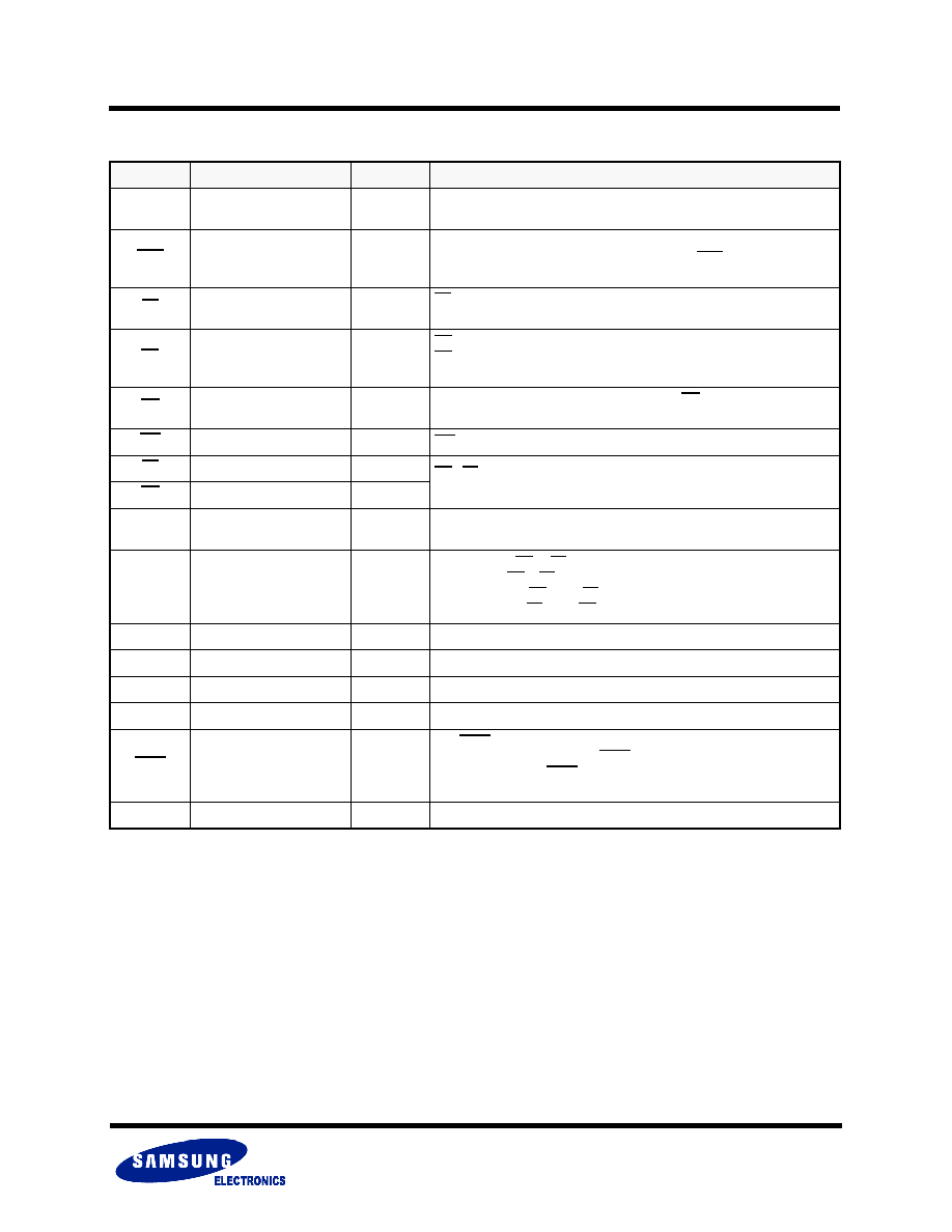
TERMINOLOGY DESCRIPTION
Name
Function
Type
Description
CLK
Clock
Input
Synchronizes the memory to the system operating frequency during syn-
chronous operations. Commands are referenced to CLK.
ADV
Address Valid
Input
Indicates that a valid address is present on the address inputs.
Addresses can be latched on the rising edge of ADV during asynchro-
nous READ and WRITE operations.
PS
Mode Register set
Input
PS low enables Mode Register to be set and enables either PAR or DPD
to be set.
CS
Chip Select
Input
CS low enables the chip to be active
CS high disables the chip and puts it into standby mode or deep power
down mode.
OE
Output Enable
Input
Enables the output buffers when LOW. when OE is HIGH, the output buff-
ers are disabled.
WE
Write Enable
Input
WE low enables the chip to start writing the data
LB
Lower Byte (I/O
0
~
7
)
Input
UB ( LB) low enables upper byte (lower byte) to allow data Input/output
from I/O buffers.
UB
Upper Byte (I/O
8
~
15
)
Input
A0~A23
Address 0 ~ Address 23
Input
Inputs for addresses during READ and WRITE operations. Addresses
are internally latched during READ and WRITE cycles.
I/O0~I/O15
Data Inputs / Outputs
Input/Output
Depending on UB or LB status,
word(16-bit, UB & LB low) data,
upper byte(8-bit, UB low & LB high) data or
lower byte(8-bit, LB low & UB high) data is loaded
V
CC
Voltage Source
Power
Device Power supply. Power supply for device core operation.
V
CCQ
I/O Voltage Source
Power
I/O Power supply. Power supply for input/output buffers.
V
SS
Ground Source
GND
Ground for device core operation
V
SSQ
I/O Ground Source
GND
Ground for input/output buffers
WAIT
Valid Data Indicator
Output
The WAIT signal is output signal indicating the status of the data on the
bus whether or not it is valid. WAIT is asserted when a burst crosses a
word-line boundary. WAIT is asserted and should be ignored during
asynchronous and page mode operations.
DNU
Do Not Use
-
-