
Revision 3.0
May 2001
K1S321615M
- 1 -
UtRAM
Document Title
2Mx16 bit Uni-Transistor Random Access Memory
The attached datasheets are provided by SAMSUNG Electronics. SAMSUNG Electronics CO., LTD. reserve the right to change the specifications and
products. SAMSUNG Electronics will answer to your questions about device. If you have any questions, please contact the SAMSUNG branch offices.
Revision History
Revision No.
0.0
0.1
1.0
2.0
3.0
Remark
Advance
Preliminary
Final
Final
Final
History
Initial Draft
- Design target
Revised
- Change package type from FBGA to TBGA.
- Improve operating current from 30mA to 25mA.
- Change input and output reference voltage from 1.1V to 1.5V at AC
test condition.
- Expand max operating voltage from 3.0V to 3.3V.
- Expand max operating temperature from 70
∞
C to 85
∞
C.
- Release speed from 70/85ns to 100ns.
- Release standby current form 170
µ
A to 200
µ
A.
- Add Power up timing diagram.
- Add AC characteristics for continuous write.
Finalize
- Release standby current form 200
µ
A to 250
µ
A.
- Release deep power down current form 10
µ
A to 20
µ
A.
- Release t
WC
for continuous write operation from 100ns to 110ns.
- Release t
CW
for continuous write operation from 90ns to 100ns.
- Release t
AW
for continuous write operation from 90ns to 100ns.
- Release t
BW
for continuous write operation from 90ns to 100ns.
- Release t
WP
for continuous write operation from 90ns to 100ns.
Revised
- Add product list
Revised
- Improve standby current from 250
µ
A to 150
µ
A.
Draft Date
September 4, 2000
February 9, 2001
March 30, 2001
April 16, 2001
May 28, 2001
Revision 3.0
May 2001
K1S321615M
- 2 -
UtRAM
PRODUCT FAMILY
Product Family
Operating Temp.
Vcc Range
Speed
(t
RC
)
Power Dissipation
PKG Type
Standby
(I
SB1
, Max.)
Deep power
down(I
SBD
, Max.)
Operating
(I
CC2
, Max.)
K1S321615M-E Extended(-25~85
∞
C)
2.7~3.3V
100ns
150
µ
A
20
µ
A
25mA
48-TBGA-9.00x12.00
2M x 16 bit Uni-Transistor CMOS RAM
GENERAL DESCRIPTION
The K1S321615M is fabricated by SAMSUNG's advanced
CMOS technology using one transistor memory cell. The device
support, extended temperature range and 48 ball Chip Scale
Package for user flexibility of system design. The device also
supports deep power down mode for low standby current.
FEATURES
∑
Process Technology: CMOS
∑
Organization: 2M x16 bit
∑
Power Supply Voltage: 2.7~3.3V
∑
Three state output status
∑
Deep Power Down: Memory cell data hold invalid
∑
Package Type: 48-TBGA-9.00x12.00
∑
Compatible with Low Power SRAM
PIN DESCRIPTION
1) Reserved for future user
Name
Function
Name
Function
CS
Chip Select Input
Vcc
Power
ZZ
Deep Power Down
Vss
Ground
OE
Output Enable Input
UB
Upper Byte(I/O
9
~
16
)
WE
Write Enable Input
LB
Lower Byte(I/O
1
~
8
)
A
0
~A
20
Address Inputs
DNU
Do Not Use
1)
I/O
1
~I/O
16
Data Inputs/Outputs
48-TBGA: Top View(Ball Down)
LB
OE
A0
A1
A2
ZZ
I/O9
UB
A3
A4
CS
I/O1
I/O10
I/O11
A5
A6
I/O2
I/O3
Vss
I/O12
A17
A7
I/O4
Vcc
Vcc
I/O13
DNU
A16
I/O5
Vss
I/O15
I/O14
A14
A15
I/O6
I/O7
I/O16
A19
A12
A13
WE
I/O8
A18
A8
A9
A10
A11
A20
1
2
3
4
5
6
A
B
C
D
E
F
G
H
SAMSUNG ELECTRONICS CO., LTD. reserves the right to change products and specifications without notice
.
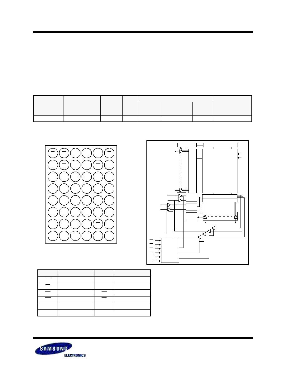
FUNCTIONAL BLOCK DIAGRAM
Clk gen.
Row
select
I/O
1
~I/O
8
Data
cont
Data
cont
Data
cont
I/O
9
~I/O
16
Vcc
Vss
Precharge circuit.
Memory array
I/O Circuit
Column select
WE
OE
UB
CS
LB
Control Logic
ZZ
Row
Addresses
Column Addresses

Revision 3.0
May 2001
K1S321615M
- 3 -
UtRAM
ABSOLUTE MAXIMUM RATINGS
1)
1. Stresses greater than those listed under "Absolute Maximum Ratings" may cause permanent damage to the device. Functional operation should be
restricted to recommended operating condition. Exposure to absolute maximum rating conditions longer than 1seconds may affect reliability.
Item
Symbol
Ratings
Unit
Voltage on any pin relative to Vss
V
IN
, V
OUT
-0.2 to V
CC
+0.3V
V
Voltage on Vcc supply relative to Vss
V
CC
-0.2 to 3.6V
V
Power Dissipation
P
D
1.0
W
Storage temperature
T
STG
-65 to 150
∞
C
Operating Temperature
T
A
-25 to 85
∞
C
FUNCTIONAL DESCRIPTION
1. X means don't care.(Must be low or high state)
CS
ZZ
OE
WE
LB
UB
I/O
1~8
I/O
9~16
Mode
Power
H
H
X
1)
X
1)
X
1)
X
1)
High-Z
High-Z
Deselected
Standby
X
1)
L
X
1)
X
1)
X
1)
X
1)
High-Z
High-Z
Deselected
Deep Power Down
L
H
X
1)
X
1)
H
H
High-Z
High-Z
Deselected
Standby
L
H
H
H
L
X
1)
High-Z
High-Z
Output Disabled
Active
L
H
H
H
X
1)
L
High-Z
High-Z
Output Disabled
Active
L
H
L
H
L
H
Dout
High-Z
Lower Byte Read
Active
L
H
L
H
H
L
High-Z
Dout
Upper Byte Read
Active
L
H
L
H
L
L
Dout
Dout
Word Read
Active
L
H
X
1)
L
L
H
Din
High-Z
Lower Byte Write
Active
L
H
X
1)
L
H
L
High-Z
Din
Upper Byte Write
Active
L
H
X
1)
L
L
L
Din
Din
Word Write
Active
ZZ=V
IL
CS=V
IH
ZZ=V
IL
CS=V
IL
, UB or/and LB=V
IL
ZZ=V
IH
CS=V
IH
, ZZ=V
IH
STANDBY MODE STATE MACHINES
Read Operation Twice
Power On
Initial State
(Wait 200
µ
s)
Active
Standby
Mode
Deep Power
Down Mode
STANDBY MODE CHARACTERISTIC
Power Mode
Memory Cell Data
Standby Current(
µ
A)
Wait Time(
µ
s)
Standby
Valid
150
0
Deep Power Down
Invaild
20
200
ZZ=V
IH
POWER UP SEQUENCE
1. Apply power.
2. Maintain stable power(Vcc min.=2.7V) for a minium 200
µ
s with CS=high.
3. Issue read operation at least twice.
CS=V
IH

Revision 3.0
May 2001
K1S321615M
- 4 -
UtRAM
DC AND OPERATING CHARACTERISTICS
1. Typical values are tested at V
CC
=3.0V,
T
A
=25
∞
C and not guaranteed.
Item
Symbol
Test Conditions
Min
Typ
1)
Max
Unit
Input leakage current
I
LI
V
IN
=Vss to Vcc
-1
-
1
µ
A
Output leakage current
I
LO
CS=V
IH,
ZZ=V
IH
, OE=V
IH
or WE=V
IL
, V
IO
=Vss to Vcc
-1
-
1
µ
A
Average operating current
I
CC1
Cycle time=1
µ
s, 100% duty, I
IO
=0mA, CS
0.2V,
ZZ
Vcc-0.2V, V
IN
0.2V or V
IN
V
CC
-0.2V
-
2
5
mA
I
CC2
Cycle time=Min, I
IO
=0mA, 100% duty, CS=V
IL
, ZZ=V
IH,
VIN=V
IL
or V
IH
-
18
25
mA
Output low voltage
V
OL
I
OL
=2.1mA
-
-
0.4
V
Output high voltage
V
OH
I
OH
=-1.0mA
2.4
-
-
V
Standby Current(CMOS)
I
SB1
CS
Vcc-0.2V, ZZ
Vcc-0.2V, Other inputs=Vss to Vcc
-
120
150
µ
A
Deep Power Down
I
SBD
ZZ
0.2V, Other inputs=Vss to Vcc
-
5
20
µ
A
RECOMMENDED DC OPERATING CONDITIONS
1)
1. T
A
=-25 to 85
∞
C, otherwise specified.
2. Overshoot: Vcc+1.0V in case of pulse width
20ns.
3. Undershoot: -1.0V in case of pulse width
20ns.
4. Overshoot and undershoot are sampled, not 100% tested.
Item
Symbol
Min
Typ
Max
Unit
Supply voltage
Vcc
2.7
3.0
3.3
V
Ground
Vss
0
0
0
V
Input high voltage
V
IH
2.2
-
Vcc+0.2
2)
V
Input low voltage
V
IL
-0.2
3)
-
0.6
V
CAPACITANCE
1)
(f=1MHz, T
A
=25
∞
C)
1. Capacitance is sampled, not 100% tested.
Item
Symbol
Test Condition
Min
Max
Unit
Input capacitance
C
IN
V
IN
=0V
-
8
pF
Input/Output capacitance
C
IO
V
IO
=0V
-
10
pF
PRODUCT LIST
Extended Temperature Products(-25~85
∞
C)
Part Name
Function
K1S321615M-EE10
48-TBGA with 48 ball, 100ns, 3.0V
Revision 3.0
May 2001
K1S321615M
- 5 -
UtRAM
AC CHARACTERISTICS
(Vcc=2.7~3.3V, T
A
=-25 to 85
∞
C)
1. The characteristics which is restricted for continuous write operation over 20 times, please refer to technical note.
2. The characteristics for continuous write operation.
Parameter List
Symbol
Speed Bins
Units
100ns
1)
100ns
2)
Min
Max
Min
Max
Read
Read Cycle Time
t
RC
100
-
100
-
ns
Address Access Time
t
AA
-
100
-
100
ns
Chip Select to Output
t
CO
-
100
-
100
ns
Output Enable to Valid Output
t
OE
-
50
-
50
ns
UB, LB Access Time
t
BA
-
100
-
100
ns
Chip Select to Low-Z Output
t
LZ
10
-
10
-
ns
UB, LB Enable to Low-Z Output
t
BLZ
10
-
10
-
ns
Output Enable to Low-Z Output
t
OLZ
5
-
5
-
ns
Chip Disable to High-Z Output
t
HZ
0
25
0
25
ns
UB, LB Disable to High-Z Output
t
BHZ
0
25
0
25
ns
Output Disable to High-Z Output
t
OHZ
0
25
0
25
ns
Output Hold from Address Change
t
OH
5
-
5
-
ns
Write
Write Cycle Time
t
WC
100
-
110
-
ns
Chip Select to End of Write
t
CW
80
-
100
-
ns
Address Set-up Time
t
AS
0
-
0
-
ns
Address Valid to End of Write
t
AW
80
-
100
-
ns
UB, LB Valid to End of Write
t
BW
80
-
100
-
ns
Write Pulse Width
t
WP
70
-
100
-
ns
Write Recovery Time
t
WR
0
-
0
-
ns
Write to Output High-Z
t
WHZ
0
30
0
30
ns
Data to Write Time Overlap
t
DW
40
-
40
-
ns
Data Hold from Write Time
t
DH
0
-
0
-
ns
End Write to Output Low-Z
t
OW
5
-
5
-
ns
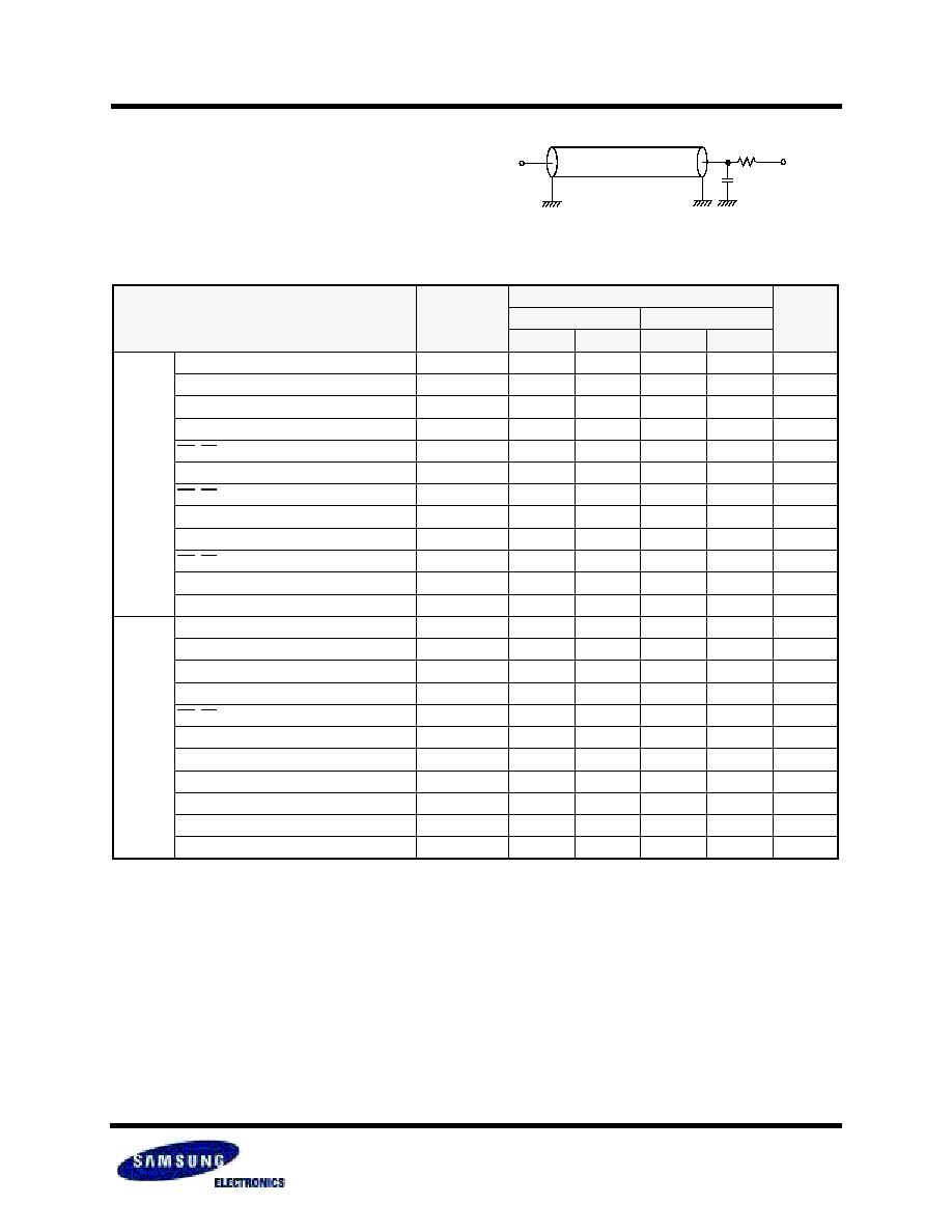
AC OPERATING CONDITIONS
TEST CONDITIONS
(Test Load and Test Input/Output Reference)
Input pulse level: 0.4 to 2.2V
Input rising and falling time: 5ns
Input and output reference voltage: 1.5V
Output load(See right): C
L
=50pF
* Include scope and jig capacitance
Dout
Z
0
=50
50pF*
R
L
=50
V
L
=1.5V
Revision 3.0
May 2001
K1S321615M
- 6 -
UtRAM
Address
Data Out
Previous Data Valid
Data Valid
TIMING DIAGRAMS
TIMING WAVEFORM OF READ CYCLE(1)
(Address Controlled
,
CS=OE=V
IL
, ZZ=WE=V
IH
, UB or/and LB=V
IL
)
TIMING WAVEFORM OF READ CYCLE(2)
(ZZ=WE=V
IH
)
t
AA
t
RC
t
OH
(READ CYCLE)
1.
t
HZ
and
t
OHZ
are defined as the time at which the outputs achieve the open circuit conditions and are not referenced to output voltage
levels.
2. At any given temperature and voltage condition,
t
HZ
(Max.) is less than
t
LZ
(Min.) both for a given device and from device to device
interconnection.
3. The minimum read cycle(
t
RC
) is determined later one of the
t
RC1
and
t
RC2.
Data Valid
High-Z
t
RC1
t
OH
t
AA
t
BA
t
OE
t
OLZ
t
BLZ
t
LZ
t
OHZ
t
BHZ
t
HZ
t
RC2
t
CO
Address
CS
UB, LB
OE
Data out
Revision 3.0
May 2001
K1S321615M
- 7 -
UtRAM
t
AS(3)
TIMING WAVEFORM OF WRITE CYCLE(1)
(WE Controlled
,
ZZ=V
IH
)
TIMING WAVEFORM OF WRITE CYCLE(2)
(CS Controlled
,
ZZ=V
IH
)
Address
Data Undefined
UB, LB
WE
Data in
Data out
t
WC
t
CW(2)
t
AW
t
BW
t
WP(1)
t
AS(3)
t
DH
t
DW
t
WHZ
t
OW
High-Z
High-Z
Data Valid
CS
Address
Data Valid
UB, LB
WE
Data in
Data out
High-Z
High-Z
t
WC
t
CW(2)
t
AW
t
BW
t
WP(1)
t
DH
t
DW
t
WR(4)
CS
t
WR(4)

Revision 3.0
May 2001
K1S321615M
- 8 -
UtRAM
TIMING WAVEFORM OF WRITE CYCLE(3)
(UB, LB Controlled
,
ZZ=V
IH
)
(WRITE CYCLE)
1. A wri
t
e occurs during the overlap(t
WP
) of low CS and low WE. A write begins when CS goes low and WE goes low with asserting UB
or LB for single byte operation or simultaneously asserting UB and LB for double byte operation. A write ends at the earliest transition
when CS goes high and WE goes high. The
t
WP
is measured from the beginning of write to the end of write.
2.
t
CW
is measured from the CS going low to the end of write.
3. t
AS
is measured from the address valid to the beginning of write.
4.
t
WR
is measured from the end of write to the address change.
t
WR
applied in case a write ends as CS or WE going high.
Address
Data Valid
UB, LB
WE
Data in
Data out
High-Z
High-Z
t
WC
t
CW(2)
t
BW
t
WP(1)
t
DH
t
DW
t
WR(4)
t
AW
t
AS(3)
CS
ZZ
MODE
Deep Power Down Mode
Normal Operation
1
µ
s
200
µ
s
Normal Operation
Read Operation Twice or Stay High during 300
µ
s
Suspend
Wake up
TIMING WAVEFORM OF DEEP POWER DOWN MODE
CS
Revision 3.0
May 2001
K1S321615M
- 9 -
UtRAM
200
µ
s
Read Operation Twice
V
CC
ZZ
CS
TIMING WAVEFORM OF POWER UP(1)
200
µ
s
V
CC
ZZ
CS
TIMING WAVEFORM OF POWER UP(2)
(No Dummy Cycle)
300
µ
s

Revision 3.0
May 2001
K1S321615M
- 10 -
UtRAM
C
1
/
2
PACKAGE DIMENSION
6
5
4
3
2
1
A
B
C
D
E
F
G
H
C
B/2
B
C
1
B
C
Bottom View
Top View
D
E
2
E
1
E
C
Side View
0
.
5
5
/
T
y
p
.
0
.
3
5
/
T
y
p
.
A
Y
Detail A
Min
Typ
Max
A
-
0.75
-
B
8.90
9.00
9.10
B1
-
3.75
-
C
11.90
12.00
12.10
C1
-
5.25
-
D
0.40
0.45
0.50
E
-
0.90
1.00
E1
-
0.55
-
E2
0.30
0.35
0.40
Y
-
-
0.08
B1
#A1
A1 INDEX MARK
Notes.
1. Bump counts: 48(8 row x 6 column)
2. Bump pitch : (x,y)=(0.75 x 0.75)(typ.)
3. All tolerence are
±
0.050 unless
otherwise specified.
4. Typ : Typical
5. Y is coplanarity: 0.08(Max)
Unit: millimeters
48 TAPE BALL GRID ARRAY(0.75mm ball pitch)
- 11 -
SAMSUNG Electronics CO., LTD. reserves the right to change products or specifications without notice.
©
2000 SAMSUNG Electronics CO., LTD.
SRAM/NVM PLANNING
YOON-000831
TNAL0001
UtRAM USAGE AND TIMING
TECHNICAL
NOTE
INTRODUCTION
UtRAM is based on single-transistor DRAM cells. As with any
other DRAM, the data in these cells must be periodically
refreshed to prevent data loss. What makes the UtRAM unique
is that it offers a true SRAM style interface that hides all refresh
operations from the memory controller.
START WITH A DRAM TECHNOLOGY
The key to the UtRAM is its high speed and low power. This
speed comes from the use of many small blocks, often just
32Kbits each, to create UtRAM arrays. The small blocks have
short word lines with little capacitance, eliminating a major
source of operating current in conventional DRAM blocks.
Each independent macro-cell on a UtRAM device consists of a
number of these blocks. Each chip has one or more macro.
The address decoding logic is also fast. UtRAM perform a
complete read operation in every tRC, but UtRAM needs power
up sequence like a DRAM.
Power Up Sequence and Diagram
1. Apply power.
2. Maintain stable power for a minium 200
µ
s with CS=high.
3. Issue read operation at least 2 times.
UtRAM USAGE AND TIMING
DESIGN ACHIEVES SRAM SPECIFIC
OPERATIONS
The UtRAM design works just like an SRAM, with no wait
states or other overhead for precharging or refreshing its inter-
nal DRAM cells. SAMSUNG Electronics(SAMSUNG) hides
these operations with advanced design. Precharging takes
place during every access, overlapped with the end of the cycle
and the decoding portion of the next cycle.
Hiding refresh is more difficult, Every row in every block must
be refreshed at least once during the refresh interval to prevent
data loss. SAMSUNG provides a internal refresh controller for
devices. When all accesses during a refresh interval are
directed to one macro-cell, as can happen in signal processing
applications, a more sophisticated approach is required to hide
refresh. The pseudo SRAM, sometimes used on these applica-
tions, which is required a memory controller that can hold off
accesses when a refresh operation is needed. SAMSUNG
unique qualitative advantage over these parts(in addition to
quantitative improvements in access speed and power con-
sumption) is that the UtRAM never needs to hold off accesses,
and indeed it has no hold off signal. The circuitry that gives
SAMSUNG this advantage is fairly simple but has not previ-
ously been disclosed.
AVOID TIMING
Following figures are show you a abonormal timing which is
not supported on UtRAM and their solution.
At read operation, if your system have a timing which sustain
invalid states over 4us at read mode like Figure 1. There are
some guide line for proper operation of UtRAM.
When your system have multiple invalid address signal shorter
than tRC on the timing which showed in Figure 1, UtRAM need
a normal read timing during that cycle(Figure 2) or toggle the
CS to 'high' about 'tRC'(Figure 3).
CS=V
IL
, UB or/and LB=V
IL
ZZ=V
IH
Read Operation(2 times)
Power On
Initial State
(Wait 200
µ
s)
Active
CS=V
IH
CS
WE
Address
Less than tRC
Over 4us
CS
WE
Address
tRC
Over 4us
Figure 2.
Put on read operation every 4us
Figure 1.
- 12 -
SAMSUNG Electronics CO., LTD. reserves the right to change products or specifications without notice.
©
2000 SAMSUNG Electronics CO., LTD.
SRAM/NVM PLANNING
YOON-000831
TNAL0001
UtRAM USAGE AND TIMING
Figure 3.
CS
WE
Address
Over 4us
tRC
toggle CS to high every 4us
CS
WE
Address
tWP
Over 4us
tWC
Write operation have similar restricted operation with Read. If
your system have a timing which sustain invalid states over 4us
at write mode and system have
continuous
write signal with Min.
tWC over 4us like Figure 4.
Figure 5.
Figure 4.
CS
WE
Address
tWP
Over 4us
tWC
tRC
Figure 6.
CS
WE
Address
tWP
Over 4us
tWC
tRC
You must put read timing on the cycle(Figure 5) or toggle the
CS to high about 'tRC'(Figure 6).
toggle CS to high every 4us
toggle WE to high and stay high at least tRC every 4us