
K3S6V2000M-TC
Synch. MROM
∑
JEDEC standard 3.3V power supply
∑
LVTTL compatible with multiplexed address
∑
Switchable organization
2,097,152 x 16(word mode) /
1,048,576 x 32(double word mode)
∑
All inputs are sampled at the rising edge of the system clock
∑
Read Performance from memory point of view
4-1-1-1 @33MHz (RAS Latency=1, CAS Latency=3)
5-1-1-1 @50MHz (RAS Latency=1, CAS Latency=4)
7-1-1-1 @66MHz (RAS Latency=2, CAS Latency=5)
t
SAC
: 10ns(Targetting 9ns)
∑
MRS cycle with address key programs
-. RAS Latency(1 & 2)
-. CAS Latency(2 ~ 6)
-. Burst Length : 4, 8
-. Burst Type : Sequential & Interleaved
∑
DQM for data-out masking
∑
Package :86TSOP2 - 400
GENERAL DESCRIPTION
FEATURES
1M x32 Synchronous MASKROM
ORDERING INFORMATION
Part NO.
MAX Freq.
Interface
Package
K3S6V2000M-TC15
66MHz
LVTTL
86TSOP2
K3S6V2000M-TC20
50MHz
K3S6V2000M-TC30
33MHz
The K3S6V2000M-TC is a synchronous high bandwidth mask
programmable ROM fabricated with SAMSUNG
s high perfor-
mance CMOS process technology and is organized either as
2,097,152 x16bit(word mode) or as 1,048,576 x32bit(double
word mode) depending on polarity of WORD pin.(see pin func-
tion description). Synchronous design allows precise cycle con-
trol, with the use of system clock, I/O transactions are possible
on every clock cycle. Range of operating frequencies, program-
mable burst length and programmable latencies allow the same
device to be useful for a variety of high bandwidth, high perfor-
mance memory system applications.
FUNCTIONAL BLOCK DIAGRAM
* Samsung Electronics reserves the right to
change products or specification without notice.
Timing Register
1M x 32
S
e
n
s
e
A
M
P
.
Column Decoder
Latency & Burst Length
Programming Register
A
d
d
r
e
s
s
R
e
g
i
s
t
e
r
R
o
w
B
u
f
f
e
r
R
o
w
D
e
c
o
d
e
r
C
o
l
.
B
u
f
f
e
r
L
R
A
S
LCKE
LRAS
LMR
CLK
CKE
MR
RAS
CAS
CS
CLK
ADD
LCAS
Output Buffer
. . .
Q0
Q16
Q15
Q31
Cell Array
DQM

K3S6V2000M-TC
Synch. MROM
PIN CONFIGURATION (TOP VIEW)
86TSOPII - 400
(0.5 mm Pin Pitch)
V
DD
Q0
V
DD
Q
Q16
Q1
VssQ
Q17
Q2
V
DD
Q
Q18
Q3
Q19
MR#
V
DD
DQM
1
2
3
4
5
6
7
8
9
10
11
12
13
14
15
16
17
18
19
20
21
22
23
24
25
26
27
28
29
30
31
32
33
34
35
36
37
38
39
40
41
42
43
77
76
75
74
73
72
71
70
69
68
67
66
65
64
63
62
61
60
59
58
57
56
55
54
53
52
51
50
49
48
47
46
45
44
86
85
84
83
82
81
80
79
78
VssQ
NC
CAS#
RAS#
CS#
A12
A11
A10
A0
WORD#
A1
A2
NC
V
DD
NC
Q4
VssQ
Q20
Q5
V
DD
Q
Q21
Q6
VssQ
Q22
Q7
V
DD
Q
Q23
V
DD
Vss
Q31
VssQ
Q15
Q30
V
DD
Q
Q14
Q29
VssQ
Q13
Q28
Q12
NC
Vss
NC
V
DD
Q
NC
NC
CLK
CKE
A8
A7
A6
A5
A4
A3
NC
Vss
NC
Q27
V
DD
Q
Q11
Q26
VssQ
Q10
Q25
V
DD
Q
Q9
Q24
VssQ
Q8
Vss
A9

K3S6V2000M-TC
Synch. MROM
PIN FUNCTION DESCRIPTION
Note1. V
DD
and V
DD
Q is same voltage.
PIN
NAME
INPUT FUNCTION
CLK
System Clock
Active on the rising edge to sample all inputs.
CS
Chip Select
Disables or enables device operation by masking or enabling all inputs except
CLK and CKE.
CKE
Clock Enable
Masks system clock to freeze operation from the next clock cycle. CKE should be
enabled at least one cycle prior to new command. Disables input buffers for power down
in standby mode.
A
0
~ A
12
Address
Row / column addresses are multiplexed on the same pins.
Row address: RA
0
~ RA
12
, column address: CA
0
~ CA
6
(x32): CA
0
~ CA
7
(x16)
RAS
Row Address Strobe
Latches row addresses on the rising edge of the CLK with RAS low.
Enables row access
CAS
Column Address Strobe
Latches column addresses on the rising edge of the CLK with CAS low.
Enables column access.
MR
Mode Register Set
Enables mode register set with MR low. (Simultaneously CS,RAS and CAS are low)
Q
0
~ Q
31
Data Output
V
DD
/V
SS
Power Supply/Ground
Power and ground for the input buffers and the core logic.
V
DD
Q
/V
SS
Q
Data Output Power/
Ground
Power and ground for the output buffers.
WORD
x32/x16 Mode Selection
Double word mode/word mode, depending on polarity of WORD pin.
Should be set before CAS enabling.
DQM
Data-out Masking
It works similar to OE during read operation.
N.C
No Connection
This pin is recommended to be left No Connection on the device.

K3S6V2000M-TC
Synch. MROM
ABSOLUTE MAXIMUM RATINGS
Note : Permanent device damage may occur if ABSOLUTE MAXIMUM RATINGS are exceeded.
Functional operation should be restricted to recommended operating condition.
Parameter
Symbol
Min
Max
Unit
Voltage on V
DD
Relative to Vss
V
DD
, V
DD
Q
-0.5
4.6
V
Voltage on Any Pin Relative to Vss
V
IN
, V
OUT
-0.5
V
DD
+ 0.5
4.6
V
Operating Temperature
T
A
0
70
∞
C
Storage Temperature
T
STG
-55
125
∞
C
Short circuit current
I
OS
-
50
mA
Power Dissipation
P
D
-
1
W
DC OPERATING CONDITIONS
Recommended operating conditions(Voltage referenced to V
SS
, T
A
=0 to 70
∞
C)
Parameter
Symbol
Min
Typ
Max
Unit
Supply Voltage
V
DD
, V
DD
Q
3.0
3.3
3.6
V
Supply Voltage(Ground)
V
SS,
V
SS
Q
0
0
0
V
DC CHARACTERISTICS
Note : 1. V
IH
(Max)=4.6V for pulse width
10ns acceptable, pulse width measured at 50% of pulse amplitude.
2. V
IL
(Min)=-1.5V for pulse width
10ns acceptable, pulse width measured at 50% of pulse amplitude.
3. The condition is the same as Self Refresh Mode of SDRAM, that is, in this case CS,RAS,CAS have to be set to Low, MR has to be set to High.
Parameter
Symbol
Min
Max
Unit
Test Condition
Standby Current ( Note3)
I
CC3P
-
150
uA
CKE
V
IL
(Max), t
CC
=Min
I
CC3PS
-
150
uA
CKE=0, t
CC
=Min
Active Standby Current
I
CC3N
-
50
mA
CS
V
IH
(Min), t
CC
=Min,
All Outputs Open
Burst Mode Operating Current
I
CC4
-
150
mA
t
CC
=Min, All Outputs Open
Input Leakage Current
I
IL
-10
10
uA
0V
V
IN
V
DD
+ 0.3V
Pins not under test=0V
Output Leakage Current (Dout Disabled)
I
OL
-10
10
uA
(0V
V
OUT
V
DD
Max)
Q# in High-Z
Input High Voltage, All Inputs
V
IH
2.0
V
DD
+ 0.3
V
(Note1)
Input Low Voltage, All Inputs
V
IL
-0.3
0.8
V
(Note2)
Output High Voltage Level (Logic 1)
V
OH
2.4
-
V
I
OH
=-2mA
Output Low Voltage Level (Logic 0)
V
OL
-
0.4
V
I
OL
=2mA
K3S6V2000M-TC
Synch. MROM
AC OPERATING TEST CONDITIONS
(T
A
= 0 to 70
∞
C, V
DD
= 3.3V
±
0.3V, unless otherwise noted.)
Note : If CLK transition time is longer than 1ns, timing parameters should be compensated. Add [(tr+tf)/2-1]ns for transition time longer than 1ns. Transi-
tion time is measured between V
IL
(Max) and V
IH
(Min).
Parameter
Value
Timing Reference Levels of Input/Output Signals
1.4V
Input Signal Levels
V
IH
/V
IL
=2.4V/0.4V
Transition Time (Rise & Fall) of Input Signals
tr/tf=1ns/1ns
Output Load
LVTTL
3.3V
1200
870
Output
50pF
V
OH
(DC)=2.4V, I
OH
=-2mA
V
OL
(DC)=0.4V, I
OL
=2mA
Vtt=1.4V
50
Output
50pF
Z
0
=50
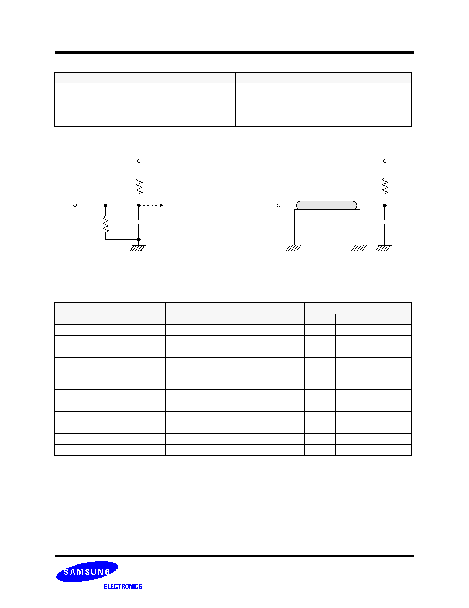
(Fig. 2) AC Output Load Circuit
(Fig. 1) DC Output Load Circuit
(AC operating conditions unless otherwise noted)
Note :
1. These t
RC
values are for BL=8. For BL=4, t
RC
=6 clks for up to 66MHz, t
RC
=5 clks for up to 50MHz, and t
RC
=5 clks for up to 33MHz. RAS latency
increase means, a simultaneous t
RC
increase in the same number of cycles.
( If RAS latency is 3 clks, t
RC
is 12 clks for BL=8.) Refer to attached technical note for gapless operation.
2. These
t
VCVC
values are for BL=8. For BL=4,
t
VCVC
=4clks for up to 66MHz,
t
VCVC
=3clks for up to 50MHz, and
t
VCVC
=2clks for up to 33MHz. Refer to
attached technical note for gapless operation.
Parameter
Symbol
up to 66MHz
up to 50 Mhz
up to 33MHz
Unit
Notes
Min
Max
Min
Max
Min
Max
CLK Cycle Time
t
CC
15
-
20
-
30
-
ns
CLK to Valid Output Delay
t
SAC
-
10
-
10
-
10
ns
Data Output Hold Time
t
OH
4
-
4
-
4
-
ns
CLK High Pulse Width
t
CH
4
-
6.5
-
11.5
-
ns
CLK Low Pulse Width
t
CL
4
-
6.5
-
11.5
-
ns
Row-active to Row-active
t
RC
10
-
9
-
9
-
clks
1
Input Setup Time
t
SS
4
-
4
-
4
-
ns
Input Hold Time
t
SH
2
-
2
-
2
-
ns
CLK to Output in Low-Z
t
SLZ
0
-
0
-
0
-
ns
CLK to Output in High-Z
t
SHZ
-
10
-
15
-
25
ns
Transition Time
t
T
0.1
10
0.1
10
0.1
10
ns
Valid CAS Enable to Valid CAS Enable
t
VCVC
8
-
7
-
6
-
clks
2
OPERATING AC PARAMETERS

K3S6V2000M-TC
Synch. MROM
CAPACITANCE
(T
A
=25
∞
C, f=1MHz)
Parameter
Symbol
Min
Max
Unit
Input Capacitance
C
IN
-
5
pF
Output Capacitance
C
OUT
-
7
pF
FUNCTION TRUTH TABLE
(V=Valid, X=Don't Care, H=Logic High, L=Logic Low)
Abbreviations (RA: Row Address, CA: Column Address, NOP: No Operation Command, DWM: Double Word Mode, WM: Word Mode)
Notes :
1. A
0
~ A
6
: Program keys (@MRS). After power up, mode register set, can be set before issuing other input command. After the mode register set com-
mand is completed, no new commands can be issued for 3 CLK Cycles, and CS or MR state must be defined "H" within 3 CLK cycles. Refer to the
Mode Register Field Table
2. In the case CKE is low, two standby modes are possible. Those are stand-by mode in power-down.
Power Down: CKE="L" (at all the parts except the range of Row Active, Read & Data out)
Clock Suspend: CKE="L" (at the range of Row Active, Read & Data Out)
3. DQM sampled at rising edge of a CLK makes a Hi-Z state the data-out state, delayed by 2CLK cycles.
4. Precharge command on Synch.DRAM can be used for Burst Stop operation during burst read operation only.
5. Mode selection control is decided simultaneously with column access start, and according to the polarity of WORD pin, "H" state is DWM,
"L" state is WM.
Command
CKEn
-1
CKEn
CS
RAS
CAS
MR
DQM
Add.
WORD
Notes
Register
Mode Register Set
H
X
L
L
L
L
X
Code
X
1
Row Active
Row Access& Latch
Row Access & Latch
H
X
L
L
H
H
X
RA
X
Read
Column Access & Latch
H
X
L
H
L
H
X
CA
X
Burst Stop
(Burst Stop on Synch.DRAM)
H
X
L
H
H
L
X
X
X
(Precharge on Synch.DRAM)
H
X
L
L
H
L
X
X
X
Power Down &
Clock Suspend
Two Standby Mode
Entry
H
L
X
X
X
X
X
X
X
2
Exit
L
H
X
X
X
X
X
X
X
DQM
H
X
V
X
3
Illegal
(Write on Synch.DRAM)
H
X
L
H
L
L
X
CA
X
(Refresh on Synch.DRAM)
H
X
L
L
L
H
X
X
X
No Operation Command
H
X
H
X
X
X
X
X
X
4
H
X
L
H
H
H
X
X
X
Organization Control
H
X
L
H
L
H
X
CA
H
5
L

K3S6V2000M-TC
Synch. MROM
Register Programmed with MRS
Address
A
6
A
5
A
4
A
3
A
2
A
1
A
0
Function
RAS Latency
CAS Latency
Burst Type
Burst Length
Burst Length
A
1
A
0
Length
0
0
Reserved
0
1
4
1
0
8
1
1
Reserved
Burst Type
A
2
Type
0
Sequential
1
Interleave
CAS Latency
A
5
A
4
A
3
Length
0
0
0
Reserved
0
0
1
2
0
1
0
3
0
1
1
4
1
0
0
5
1
0
1
6
1
1
0
Reserved
1
1
1
Reserved
RAS
A
6
Type
0
1
1
2
Notes :
-. After power up, when user wants to change mode register set, user must exit from power down mode
and start mode register set before entering normal operation mode.
MODE REGISTER FIELD TABLE TO PROGRAM MODES
(3) Each address is arranged as follows
for X32 operation
,
for X16 operation,
when CA7 is set to Low, data belonging to 0~15th registers are output to Q0~Q15 pins, and when CA7 is set to High, data belonging
to16~31th registers are output to Q0~Q15 pins.
Address Register
AR19
AR18
AR17
...
AR8
AR7
AR6
...
AR3
AR2
AR1
AR0
Address
RA12
RA11
RA10
...
RA1
RA0
CA6
...
CA3
CA2
CA1
CA0
(1) WORD = "H" : x32 Organization
Note : Column Address MSB (at x32 organization) (X=Don't Care)
Function
A
0
A
1
A
2
A
3
A
4
A
5
A
6
A
7
A
8
A
9
A
10
A
11
A
12
Row Address
RA
0
RA
1
RA
2
RA
3
RA
4
RA
5
RA
6
RA
7
RA
8
RA
9
RA
10
RA
11
RA
12
Column Address
CA
0
CA
1
CA
2
CA
3
CA
4
CA
5
CA
6
Note
X
X
X
X
X
X
(2) WORD="L" : x16 Organization
Note : Column Address MSB (at x16 organization) (X=Don't Care)
Function
A
0
A
1
A
2
A
3
A
4
A
5
A
6
A
7
A
8
A
9
A
10
A
11
A
12
Row Address
RA
0
RA
1
RA
2
RA
3
RA
4
RA
5
RA
6
RA
7
RA
8
RA
9
RA
10
RA
11
RA
12
Column Address
CA
0
CA
1
CA
2
CA
3
CA
4
CA
5
CA
6
CA
7
Note
X
X
X
X
X
ADDRESSING MAP
* Initial Address
- BL=4(CA0,CA1)
- BL=8(CA0,CA1,CA2)
BL=8
BL=4
MSB
LSB

K3S6V2000M-TC
Synch. MROM
BURST SEQUENCE(BURST LENGTH = 4)
Initial address
Sequential
Interleave
A1
A0
0
0
0
1
2
3
0
1
2
3
0
1
1
2
3
0
1
0
3
2
1
0
2
3
0
1
2
3
0
1
1
1
3
0
1
2
3
2
1
0
x32 operation (double word mode)
Column Address
D15 ~ D0 (Hexadecimal)
D31 ~ D16 (Hexadecimal)
CA6
CA5
CA4
CA3
CA2
CA1
CA0
0
0
0
0
0
0
0
A
A
A
A
0
0
0
0
0
0
0
0
0
0
1
B
B
B
B
1
1
1
1
0
0
0
0
0
1
0
C
C
C
C
2
2
2
2
0
0
0
0
0
1
1
D
D
D
D
3
3
3
3
0
0
0
0
1
0
0
E
E
E
E
4
4
4
4
0
0
0
0
1
0
1
F
F
F
F
5
5
5
5
x16 operation (word mode)
Column Address
Data Out (Hexadecimal)
Comment
CA7
CA6
CA5
CA4
CA3
CA2
CA1
CA0
0
0
0
0
0
0
0
0
A
A
A
A
D15 ~ D0
0
0
0
0
0
0
0
1
B
B
B
B
D15 ~ D0
0
0
0
0
0
0
1
0
C
C
C
C
D15 ~ D0
0
0
0
0
0
0
1
1
D
D
D
D
D15 ~ D0
0
0
0
0
0
1
0
0
E
E
E
E
D15 ~ D0
0
0
0
0
0
1
0
1
F
F
F
F
D15 ~ D0
:
1
0
0
0
0
0
0
0
0
0
0
0
D31 ~ D16
1
0
0
0
0
0
0
1
1
1
1
1
D31 ~ D16
1
0
0
0
0
0
1
0
2
2
2
2
D31 ~ D16
BURST SEQUENCE(BURST LENGTH = 8)
Initial address
Sequential
Interleave
A2
A1
A0
0
0
0
0
1
2
3
4
5
6
7
0
1
2
3
4
5
6
7
0
0
1
1
2
3
4
5
6
7
0
1
0
3
2
5
4
7
6
0
1
0
2
3
4
5
6
7
0
1
2
3
0
1
6
7
4
5
0
1
1
3
4
5
6
7
0
1
2
3
2
1
0
7
6
5
4
1
0
0
4
5
6
7
0
1
2
3
4
5
6
7
0
1
2
3
1
0
1
5
6
7
0
1
2
3
4
5
4
7
6
1
0
3
2
1
1
0
6
7
0
1
2
3
4
5
6
7
4
5
2
3
0
1
1
1
1
7
0
1
2
3
4
5
6
7
6
5
4
3
2
1
0

K3S6V2000M-TC
Synch. MROM
CLOCK (CLK)
The clock input is used as a reference for SMROM operation. A square wave signal(CLK) must be applied externally at cycle time
t
CC.
All operations are synchronized to the rising edge of the clock. The clock transitions must be monotonic between V
IL
and V
IH
.
During operation with CKE high, all inputs are assumed to be in valid state (low or high) for the duration of set-up and hold time
around the positive edge of the clock for proper functionality and I
CC
specifications.
CLOCK ENABLE (CKE)
The clock enable(CKE) gates the clock into the SMROM and is asserted high during all cycles, except for power down, stand-by and
clock suspend mode. If CKE goes low synchronously with clock (set-up and hold time same as other inputs), the internal clock is sus-
pended from the next clock cycle and the state of output and burst address is frozen for as long as the CKE remains low. All other
inputs are ignored from the next clock cycle after CKE goes low. The SMROM remains in the power down mode ignoring other inputs
for as long as CKE remains low. The power down exit is synchronous as the internal clock is suspended. When CKE goes high at
least "1 CLK + t
SS
" before the rising edge of the clock, then the SMROM becomes active from the same clock edge accepting all the
input commands.
NOP and DEVICE DESELECT
When RAS, CAS and MR are high, the SMROM performs no operation (NOP). NOP does not initiate any new operation. Device
deselect is also a NOP and is entered by asserting CS high. CS high disables the command decoder so that RAS, CAS, MR and all
the address inputs are ignored. In addition, entering a mode register set command in the middle of a normal operation, results in an
illegal state in SMROM.
POWER-UP
The following power-up sequence is recommended.
1. Apply power and start clock, Attempt to maintain MR, CKE and DQM inputs to pull them high and the other pins are NOP condition
at the inputs before or along with V
DD
(and V
DD
Q) supply.
2. Maintain stable power, stable clock and NOP input condition for a minimum of 20us.
3. When user wants to change the default mode register set values, perform a MODE REGISTER SET cycle to program the RAS
latency, CAS latency, burst length and burst type.
4. At the end of three clock cycles after the mode register set cycle, the device is ready for operation. When the above sequence is
used for power-up, all outputs will be in high impedance state. The high impedance of outputs is not guaranteed in any other
power-up sequence.
MODE SELECTION CONTROL
Mode selection control is decided simultaneously with column access, and according to WORD pin voltage level. High level signifies
double word mode(x32) and low level signifies word mode(x16).
ADDRESS DECODING
The address bits required to decode one of the available cell locations out of the total depth are multiplexed onto the address select
pins and latched by externally applying two commands. The first command, RAS asserted low, latches the row address into the
device. A second command, CAS asserted low, subsequently latches the column address.
DEVICE OPERATIONS

K3S6V2000M-TC
Synch. MROM
MODE REGISTER SET (MRS)
The mode register stores the data for controlling the various operating modes of SMROM. It programs the RAS latency, CAS latency,
burst length, burst type. The default value of the mode register is defined as RAS latency=2, CAS latency=5, Burst length=4,
Sequential Burst Type. When and if the user wants to change its values, the user must exit from power down mode and start mode
register set before entering normal operation mode. The mode register is reprogrammed by asserting low on CS, RAS, CAS and MR
(The SMROM should be in active mode with CKE already high prior to writing the mode register). The state of address pins A
0
~ A
6
in the same cycle as CS, RAS, CAS and MR going low is the data written in the mode register. Three clock cycles are required to
complete the program in the mode register, therefore after mode register set command is completed, no new commands can be
issued for 3 clock cycles and CS or MR must be fixed to high within 3 clock cycles. The mode register is divided into various fields
depending on functionality. The burst length field uses A
0
~ A
1
, burst type uses A
2
, CAS latency (read latency from column address)
uses A
3
~ A
5,
RAS latency uses
A
6
(RAS to CAS delay). Refer to the table for specific codes for various burst length, burst type, CAS
latencies and RAS latencies.
LATENCY
There are latencies between the issuance of a Row active command and when data is available on the I/O buffers. The RAS to CAS
delay is defined as the RAS latency. The CAS to data out delay is the CAS latency. The CAS and RAS latencies are programmable
through the mode register. RAS latencies of 1 and 2, and CAS latencies of 2 through 6 are supported. It is understood that some
RAS and CAS latency values are reserved for future use, and may not be available in the first generation for SMROM. The followings
are the supported minimum values in the first generation. RAS latency=2, and CAS latency=5 for 66MHz operation, and RAS
latency=1, and CAS latenecy=4 for 50MHz operation, and RAS latency=1, and CAS latenecy=3 for 33MHz operation.
DQM OPERATION
The DQM is used to mask output operations when a complete burst read is not required. It works similar to OE during a read opera-
tion. The read latency is two cycles from DQM, which means DQM masking occurs two cycles later in the read cycle. DQM operation
is synchronous with the clock. The masking occurs for a complete cycle. (Also refer to the DQM timing diagram)
BURST READ
The burst read command is used to access a burst of data on consecutive clock cycles from an active row state. The burst read com-
mand is issued by asserting low CS and CAS with MR being high on the rising edge of the clock. The first output appears in CAS
latency number of clock cycles after the issuance of the burst read command. The burst length, burst sequence and latency from the
burst read command are determined by the mode register which is already programmed. Burst read can be initiated on any column
address of the active row. The output goes into high-impedance at the end of the burst, unless a new burst read is initiated to keep
the data output gapless. The burst read can be terminated by issuing another burst read.
DEVICE OPERATIONS

K3S6V2000M-TC
Synch. MROM
D
0
Internal
CLK
Internal
CLK
CKE
Internal
CLK
Note :
1. After mode register set command is completed, no new commands can be issued for 3 clock cycles, and MR or CS should be fixed "H"
within a minimum of 3 clock cycles.
BASIC FEATURE AND FUNCTION DESCRIPTIONS
1. MRS
Mode Register Set
CLK
CMD
MRS
ACT
Note 1
3CLK
2. CLOCK Suspend
Clock Suspended During Burst Read (BL=4)
Masked by CKE
Q
0
Q
1
Q
2
Q
3
Suspended Dout
CLK
CMD
RD
CKE
Data
3. Clock Suspend Exit & power Down Exit
1) Clock Suspend Exit
CLK
CKE
CMD
RD
2) Power Down Exit
CLK
CMD
NOP
ACT
t
SS
t
SS
: This command do not be activated.

K3S6V2000M-TC
Synch. MROM
Q
0
Q
1
Q
3
Q
0
Q
2
Q
3
Q
1
Q
2
Q
3
Masked by DQM
Q
0
D
1
Q
1
Q
8
Q
3
Q
0
Q
7
Q
8
Q
2
Q
6
Q
7
Q
1
*Note :
1. DQM makes data out Hi-Z after 2CLKs which should masked by CKE " L"
Q
7
Q
6
Q
5
4. DQM Operation
CLK
CMD
DQM
Data(CL2)
Data(CL3)
Data(CL4)
RD
CLK
CMD
DQM
CKE
RD
1) Read Mask (BL=4)
2) DQM with Clock Suspended (BL=8)
Hi-Z
Hi-Z
Hi-Z
Q
5
Q
4
Q
3
Hi-Z
Hi-Z
Hi-Z
Hi-Z
Hi-Z
Hi-Z
DQM to Data-out Mask = 2CLKs
Hi-Z
Hi-Z
Hi-Z
Note 1
Data(CL2)
Data(CL3)
Data(CL4)

K3S6V2000M-TC
Synch. MROM
0
1
2
3
4
5
6
7
8
9
10
11
12
13
14
15
16
17
18
19
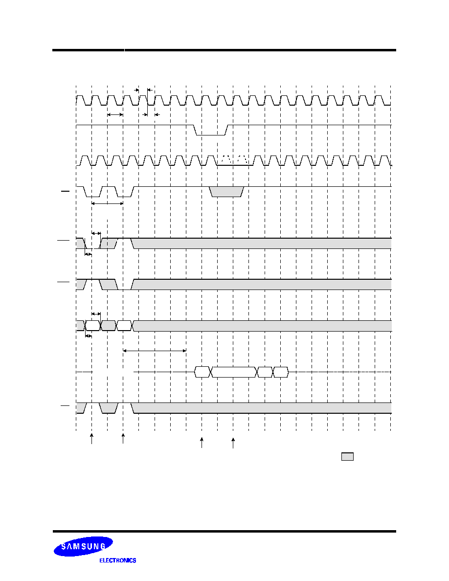
Read Cycle I : Normal @RAS Latency=2, CAS Latency=5, Burst Length=4
t
SS
t
SH
CKE
CS
RAS
CAS
ADDR
Data
t
CH
t
CC
t
CL
HIGH
t
SH
t
SS
t
SHZ
t
SAC
t
OH
Qa0 Qa1 Qa2 Qa3
CAb
RAb
*Note:
1. When the burst length is 4 at 66MHz, t
RC
is equal to 6 clock cycles.
RAS
Latency
MR
*Note 1
t
RC
=6 clocks at BL=4
Row Active
Read
Row Active
Read
:
Don't Care
t
SS
t
SH
Qb0 Qb1 Qb2 Qb3
CAa
RAa
CLK
t
RC

K3S6V2000M-TC
Synch. MROM
0
1
2
3
4
5
6
7
8
9
10
11
12
13
14
15
16
17
18
19
Read Cycle II : Consecutive Column Access @RAS Latency = 2, CAS Latency=5, BL = 4
t
SS
t
SH
t
SS
t
SH
CKE
CS
RAS
CAS
ADDR
Data
t
CH
t
CC
t
CL
HIGH
t
SH
t
SS
CAa
RAa
t
SHZ
t
SAC
t
OH
Qb1 Qb2 Qb3
CAb
Note:
When column access is initiated beyond t
VCVC,
1. at BL=4, CAa access read is completed, CAb access read begins.
Qb0
RAS
Latency
t
VCVC
=4 clocks at BL=4
Burst Length=4
Qa1 Qa2 Qa3
Qa0
MR
Row Active
Read
Read
: Don't Care
CLK
*Note 1
K3S6V2000M-TC
Synch. MROM
0
1
2
3
4
5
6
7
8
9
10
11
12
13
14
15
16
17
18
19
Read Cycle III : Clock Suspend @RAS Latency = 2, CAS Latency=5, Burst Length=4
t
SS
t
SH
CKE
CS
RAS
CAS
ADDR
Data
t
CH
t
CC
t
SH
t
SS
CAa
RAa
Note :
1. From next clock after CKE goes low, clock suspension begins.
2. For clock suspension, data output state is held & maintained.
RAS
Latency
t
VCVC
= 4 clocks at BL=4
*Note 2
Burst Length=4
Qa2 Qa3
*Note 1
MR
Row Active
Read
Clock Suspend Resume
:
Don't Care
Qa1
CLK
Internal
CLK
t
CL
Qa0

K3S6V2000M-TC
Synch. MROM
0
1
2
3
4
5
6
7
8
9
10
11
12
13
14
15
16
17
18
19
Read Interrupted by Precharge Command & Burst Read Stop Cycle @Burst Length=8
*Note :
1. The burst stop command is valid at every page burst length.
The data bus goes to High-Z after the CAS latency from the burst stop command is issued.
2. The interval between read command (column address presented) and burst stop command is 1 cycle(min).
HIGH
CL=3
ADDR
CAS
RAS
CS
CKE
CLK
MR
DQM
Qa0 Qa1 Qa2
Qa4
Qb0 Qb1 Qb2 Qb3 Qb4 Qb5
RAa
CAa
CAb
Row Active
Precharge
Burst Stop
Read
Read
:
Don't Care
Note1
CL=2
Data
Qa0 Qa1 Qa2
Qa4
Qb0 Qb1 Qb2 Qb3 Qb4 Qb5
Qa3
Qa3
*Note1, 2
Note1
Note2
Note2

K3S6V2000M-TC
Synch. MROM
0
1
2
3
4
5
6
7
8
9
10
11
12
13
14
15
16
17
18
19
Power Down & Clock Suspend Cycle :
CKE
CS
RAS
CAS
ADDR
Data
Power Down
Read
Clock Suspend
CAa
RAa
@RAS Latency = 2, CAS Latency=5, Burst Length=4
Qa1
Qa2
Qa0
MR
Qa3
Row Active
(High)
Data Hi-Z State
CLK
(internal)
NOP
Power-down
Clock Suspend
Entry
Entry
Power-down
Exit
Clock Suspend
Exit
Note :
1. From next clock after CKE goes low, clock suspend and power down begins.
2. After power down exit, NOP should be issued and new command can be issued after 1clock.
:
Don't Care
t
SS
t
SH
*Note 2
*Note 1
t
SS
*Note 1

K3S6V2000M-TC
Synch. MROM
0
1
2
3
4
5
6
7
8
9
10
11
12
13
14
15
16
17
18
19
Mode Register Set:
t
SS
t
SH
CKE
CS
RAS
CAS
ADDR
Data
MR
t
CH
t
CC
t
CL
HIGH
Code
RAa
Note :
1. After the mode register set is completed, no new commands can be issued for 3CLK cycles.
2. After power up, necessarily mode register set should be completed at least one time and CS or MR must be fixed "H" within
3clock cycles, and when user wants to change mode register set, user must exit from power down mode and start mode reg-
ister set before chip enters normal operation mode.
RAS
Latency
Data Hi-Z State
MRS
Row Active
:
Don't Care
CAa
Qa0 Qa1 Qa2 Qa3
@RAS Latency = 2, CAS Latency=5, Burst Length=4
CLK

K3S6V2000M-TC
Synch. MROM
FUNCTION TRUTH TABLE
* : After the power up, when user wants to change MR set, user must exit from power down mode and start MR set before chip enters normal operation
mode.
Current
State
Input Signal
Next State Operation
CKE
CS
RAS
CAS
MR
Add.
After
Power Up*
L
X
X
X
X
X
-. Power Down
H
L
L
H
H
RA
-. Row Active ; latch RA
H
L
L
L
L
Code
-. Mode Register Set
Row Active
H
L
L
H
H
RA
-. If consecutive row access is issued within
t
RCmin.
without CAS enabling, only the final
RA is valid.
H
L
H
L
H
CA
-. Begin READ ; latch CA
H
L
L
L
L
Code
Illegal *
L
X
X
X
X
X
-. Clock Suspend
READ
H
L
L
H
H
RA
-. Row Access in Read State,
within the tRC, previous read is ignored and
new row is activated.
beyond the tRC, previous read is completed
and new read begins.
H
L
H
L
H
CA
-. Consecutive Column Access,
within the t
VCVC
, only the final CA is valid
and the previous burst read is ignored.
Beyond the t
VCVC
, the previous read is
completed and new read begins.
H
L
L
H
L
X
-. NOP (After Burst Read) / Read Interrupt
H
L
H
H
L
X
-. NOP (After Burst Read) / Read Interrupt
H
L
L
L
L
Code
Illegal *
L
X
X
X
X
X
-. Clock Suspend / Power Down
Any State
L
L
L
L
H
X
-. Low Power Consumption Mode
Any State
H
L
H
H
H
X
NOP
Any State
H
L
L
L
H
X
Illegal
H
L
H
L
L
CA
Illegal

K3S6V2000M-TC
Synch. MROM
#86
22.22
±
0.10
0.875
±
0.004
MAX
22.62
0.891
MAX
1.00
±
0.10
0.039
±
0.004
1.20
0.047
MIN
0.010
0.05
0.004 MAX
0.10 MAX
#1
0.61
( )
0.024
1
0
.
1
6
0
.
4
0
0
0.50
0.020
+0.075
0.125
-0.035
+0.004
0.005
-0.002
1
1
.
7
6
±
0
.
2
0
0
.
4
6
3
±
0
.
0
0
8
#44
0.50
0.0197
+0.10
0.20
-0.03
0~8
∞
#43
0
.
4
5
~
0
.
7
5
0
.
0
1
8
~
0
.
0
3
0
0.21
±
0.05
0.008
±
0.002
(Unit : mm/inch)
PACKAGE DIMENSIONS
86-TSOP2-400

K3S6V2000M-TC
Synch. MROM
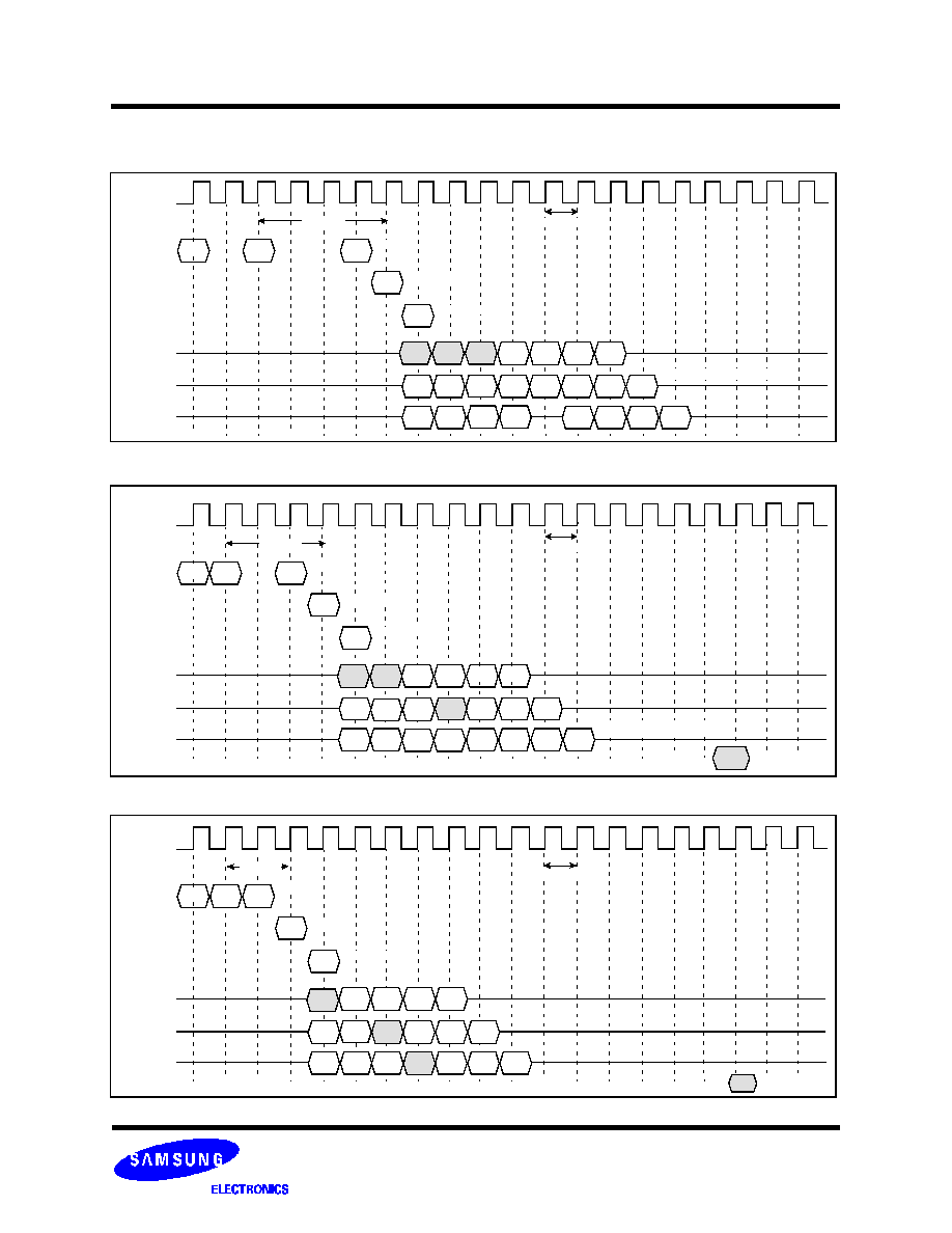
K3S6V2000M-TC15
Burst Length
RAS Latency
CAS Latency
tRCmin.
tVCVCmin.
4
2
5
6
4*
6
7
5
8
2
5
10
8*
6
11
9
Technical Notes
( unit : number of clock )
K3S6V2000M-TC20
Burst Length
RAS Latency
CAS Latency
tRCmin.
tVCVCmin.
4
1
4
4*
3/ 4*
5
5
4*
6
6
5
8
1
4
8*
7/ 8*
5
9
8*
6
10
9
( unit : number of clock )
K3S6V2000M-TC30
Note :
Above tables are not specifications values, rather actual values.
There are no gapless operations for CAS latency 6,7 and 8.
* : Minimum clocks for Gapless Operation.
Burst Length
RAS Latency
CAS Latency
tRCmin.
tVCVCmin.
4
1
3
3/
4*
2/ 4*
4
4*
3/
4*
5
5
4*
8
1
3
7/
8*
6/
8
*
4
8*
7/
8
*
5
9
8*
( unit : number of clock )
1. Frequency vs. AC Parameter Relationship Table

K3S6V2000M-TC
Synch. MROM
RD
PRE
Q
0
Q
0
Q
1
Q
0
Q
1
RD
Q
0
Q
1
Q
0
Q
1
Q
0
Q
1
Q
1
3. Read interrupt operation by issuing the precharge or Burst Stop Command
CLK
CMD
CLK
CMD
QB
1
QB
2
RD
QB
3
RD
A
B
QB
0
QB
1
QB
2
QB
3
QB
0
QB
1
QB
2
QB
3
QB
0
Note 2
Data(CL2)
Data(CL3)
Data(CL4)
*Note :
1. By " Interrupt", It is meant to stop burst read by external command before the end of burst.
By "CAS Interrupt", to stop burst read by CAS access.
2. CAS to CAS delay. (=1CLK)
2. CAS Interrupt
Read interrupted by Read (BL=4)
Note 1
CLK
CMD
ADD
CASE I ) Issued read Interrupt command during burst read operation period.
RD
PRE
Q
0
Q
0
Q
0
Note 2
RD
STOP
Q
0
Q
0
Q
0
CLK
CMD
CLK
CMD
CASE II ) Issued read Interrupt command between read command and data out.
*Note :
1. The data bus goes to High-Z after CAS Latency from the burst stop (or precharge) command.
2. Valid output data will last up to CL-1 clock cycle from PRE command.
Note 2
Note 1
Note 1
Technical Notes
(Continuous)
Data(CL2)
Data(CL3)
Data(CL4)
Data(CL2)
Data(CL3)
Data(CL4)
Data(CL2)
Data(CL3)
Data(CL4)
Data(CL2)
Data(CL3)
Data(CL4)
STOP

K3S6V2000M-TC
Synch. MROM
RDa
4. Read cycle depending on t
RC
@ RL = 2, CL = 5, BL = 4 ; 66MHz
tRC(min)=6
ACT
tCC=15ns
RDb
ACT
RDb
Qb
1
Qb
2
Qb
3
Qb
0
Qb
1
Qb
2
Qb
3
Qb
0
Qa
1
Qa
2
Qa
0
Qa
3
Qa
1
Qa
2
Qa
0
Qa
3
High-Z
CASE I )
RDb
ACT
CASE II )
CASE III )
ACT
@ RL = 1, CL = 4, BL = 4 ; 50MHz
tRC(min)=4
ACT
tCC=20ns
ACT
Qb
1
Qb
2
Qb
3
Qb
0
Qb
1
Qb
2
Qb
3
Qb
0
Qa
1
Qa
2
Qa
0
Qa
3
Qa
1
Qa
2
Qa
0
Qa
3
CASE I )
ACT
CASE II)
CASE III)
ACT
@ RL = 1, CL = 3, BL = 4 ; 33MHz
tRC(min)=3
ACT
tCC=30ns
ACT
Qb
1
Qb
2
Qb
3
Qb
0
Qb
2
Qb
3
Qb
1
Qa
1
Qa
0
Qa
2
Qa
1
Qa
2
Qa
0
Qa
3
CASE I)
ACT
CASE II)
CASE III)
ACT
Qb
1
Qb
2
Qb
3
Qb
0
Qb
1
Qb
2
Qb
3
Qb
0
Qb
1
Qb
2
Qb
3
Qb
0
: Invalid Data
CLK
CMD
CASE I )
CASE II )
CASE III )
CLK
CMD
CASE I )
CASE II )
CASE III )
CLK
CMD
CASE I )
CASE II )
CASE III )
RDa
RDb
RDb
RDb
RDa
RDb
RDb
RDb
(Gapless Operation)
(Gapless Operation)
K3S6V2000M-TC
Synch. MROM
5. Read cycle depending on tVCVC
@ RL = 2, CL = 5, BL = 4 ; 66MHz
tVCVC=4
ACT
Qb
1
Qb
2
Qb
3
Qb
0
CASE I)
CASE II)
CASE III)
CLK
CMD
CASE I )
CASE II )
CASE III )
Qb
1
Qb
2
Qb
3
Qb
0
Qb
1
Qb
2
Qb
3
Qb
0
Qa
0
Qa
1
Qa
0
@ RL = 1, CL = 4, BL = 4 ; 50MHz
tVCVC=3
ACT
Qb
1
Qb
2
Qb
3
Qb
0
CASE I)
CASE II)
CASE III)
CLK
CMD
CASE I )
CASE II )
CASE III )
Qb
1
Qb
2
Qb
3
Qb
1
Qb
2
Qb
3
Qb
0
Qa
0
Qa
1
Qa
0
@ RL = 1, CL = 3, BL = 4 ; 33MHz
tVCVC=2
ACT
Qb
1
Qb
2
Qb
3
Qb
0
CASE I)
CASE II)
CASE III)
CLK
CMD
CASE I )
CASE II )
CASE III )
Qb
1
Qb
2
Qb
3
Qb
1
Qb
2
Qb
3
Qa
0
Qa
1
Qa
0
RDa
RDb
RDb
RDb
RDa
RDb
RDb
RDb
RDa RDb
RDb
RDb
Qa
2
Qa
3
Qa
1
Qa
3
Qa
2
(Gapless Operation)
(Gapless Operation)
: Invalid Data
: Invalid Data
Qa
3
Qa
2
Qa
2
Qa
1
Qa
2
Qa
1
tCC=15ns
tCC=20ns
tCC=30ns

K3S6V2000M-TC
Synch. MROM
6. Read Cycle depending on t
VCVC
and t
RC
@ RL = 1, CL = 4, BL = 4 ; 50MHz (Gapless Operation)
tVCVC=4
ACT
CLK
CMD
Read out
Qc
0
Qc
1
Qa
0
@ RL = 1, CL = 4, BL = 4 ; 50MHz
CLK
@ RL = 1, CL = 4, BL = 4 ; 50MHz
CLK
RDa
RDb
Qa
2
Qa
1
: Invalid Data
ACT RDc
RDd
tCC=20ns
tCC=20ns
tCC=20ns
Qc
2
ACT RDe
RDf
Qe
0
: Invalid Data
CMD
Read out
Qc
0
Qc
1
Qa
0
Qa
2
Qa
1
RDd
Qc
2
ACT RDe
RDf
Qe
0
Qe
1
Qe
2
Qa
3
Qc
3
ACT
CMD
Read out
Qb
2
Qb
3
Qa
0
RDa
RDb
Qa
2
Qa
1
ACT RDc
RDd
Qc
0
ACT RDe
Qd
0
Qd
1
Qd
2
Qa
3
Qb
1
Qb
0
Qc
1
Qc
2
Qc
3
tVCVC=4
tVCVC=4
ACT RDa
RDb ACT RDc