K3S7V2000M-TC
Synch. MROM
∑
JEDEC standard 3.3V power supply
∑
LVTTL compatible with multiplexed address
∑
Address: Row address: RA
0
~ RA
12
Column address: CA
0
~ CA
7
(x32): CA
0
~ CA
8
(x16)
∑
Switchable organization
4,194,304 x 16(word mode) /
2,097,152 x 32(double word mode)
∑
All inputs are sampled at the rising edge of the system clock
∑
Read Performance at memory point of view
@33MHz 4-1-1-1 (RAS Latency=1, CAS Latency=3)
@50MHz 5-1-1-1 (RAS Latency=1, CAS Latency=4)
@66MHz 5-1-1-1 (RAS Latency=1, CAS Latency=4)
@83MHz 7-1-1-1 (RAS Latency=2, CAS Latency=5)
@100MHz 7-1-1-1 (RAS Latency=2, CAS Latency=5)
∑
t
SAC
: 6ns
∑
Default mode by user requirement
∑
MRS cycle with address key programs
-. RAS Latency(1 & 2)
-. CAS Latency(3 ~ 6)
-. Burst Length : 4, 8
-. Burst Type : Sequential & Interleaved
∑
DQM for data-out masking
∑
Package :86TSOP2 - 400
GENERAL DESCRIPTION
FEATURES
64M-Bit (4Mx16 /2Mx32) Synchronous MASKROM
ORDERING INFORMATION
Part NO.
MAX Freq.
Interface
Package
K3S7V2000M-TC10
100MHz
LVTTL
86TSOP2
K3S7V2000M-TC12
83MHz
K3S7V2000M-TC15
66MHz
K3S7V2000M-TC20
50MHz
K3S7V2000M-TC30
33MHz
The K3S7V2000M-TC is a synchronous high bandwidth mask
programmable ROM fabricated with SAMSUNG
s high perfor-
mance CMOS process technology and is organized either as
4,194,304 x16bit(word mode) or as 2,097,152 x32bit(double
word mode) depending on polarity of WORD pin.(see pin func-
tion description). Synchronous design allows precise cycle con-
trol, with the use of system clock, I/O transactions are possible
on every clock cycle. Range of operating frequencies, program-
mable burst length and programmable latencies allow the same
device to be useful for a variety of high bandwidth, high perfor-
mance memory system applications.
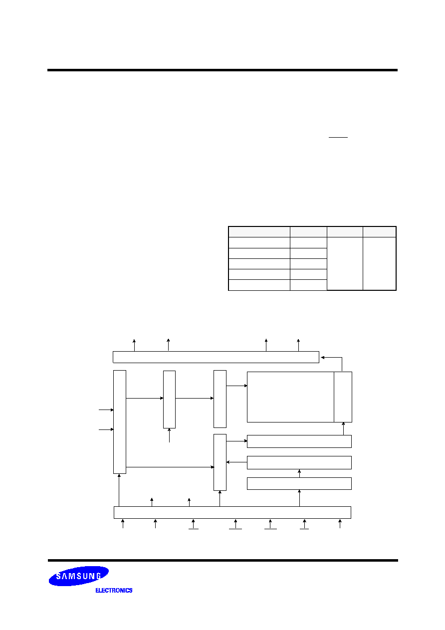
FUNCTIONAL BLOCK DIAGRAM
* Samsung Electronics reserves the right to
change products or specification without notice.
Timing Register
4M x 16 /2M x 32
S
e
n
s
e
A
M
P
.
Column Decoder
Latency & Burst Length
Programming Register
A
d
d
r
e
s
s
R
e
g
i
s
t
e
r
R
o
w
B
u
f
f
e
r
R
o
w
D
e
c
o
d
e
r
C
o
l
.
B
u
f
f
e
r
L
R
A
S
LCKE
LRAS
LMR
CLK
CKE
MR
RAS
CAS
CS
CLK
ADD
LCAS
Output Buffer
. . .
Q0
Q16
Q15
Q31
Cell Array
DQM

K3S7V2000M-TC
Synch. MROM
PIN CONFIGURATION (TOP VIEW)
86TSOPII - 400
(0.5 mm Pin Pitch)
V
DD
Q0
V
DD
Q
Q16
Q1
VssQ
Q17
Q2
V
DD
Q
Q18
Q3
Q19
MR#
V
DD
DQM
1
2
3
4
5
6
7
8
9
10
11
12
13
14
15
16
17
18
19
20
21
22
23
24
25
26
27
28
29
30
31
32
33
34
35
36
37
38
39
40
41
42
43
77
76
75
74
73
72
71
70
69
68
67
66
65
64
63
62
61
60
59
58
57
56
55
54
53
52
51
50
49
48
47
46
45
44
86
85
84
83
82
81
80
79
78
VssQ
NC
CAS#
RAS#
CS#
A12
A11
A10
A0
WORD#
A1
A2
NC
V
DD
NC
Q4
VssQ
Q20
Q5
V
DD
Q
Q21
Q6
VssQ
Q22
Q7
V
DD
Q
Q23
V
DD
Vss
Q31
VssQ
Q15
Q30
V
DD
Q
Q14
Q29
VssQ
Q13
Q28
Q12
NC
Vss
NC
V
DD
Q
NC
NC
CLK
CKE
A8
A7
A6
A5
A4
A3
NC
Vss
NC
Q27
V
DD
Q
Q11
Q26
VssQ
Q10
Q25
V
DD
Q
Q9
Q24
VssQ
Q8
Vss
A9
K3S7V2000M-TC
Synch. MROM
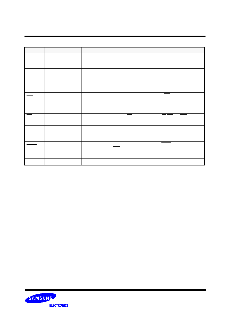
PIN FUNCTION DESCRIPTION
Note1. V
DD
and V
DD
Q is same voltage.
PIN
NAME
INPUT FUNCTION
CLK
System Clock
Active on the rising edge to sample all inputs.
CS
Chip Select
Disables or enables device operation by masking or enabling all inputs except
CLK and CKE.
CKE
Clock Enable
Masks system clock to freeze operation from the next clock cycle. CKE should be
enabled at least one cycle prior to new command. Disables input buffers for power down
in standby mode.
A
0
~ A
12
Address
Row / Column addresses are multiplexed on the same pins.
Row address: RA
0
~ RA
12
, Column address: CA
0
~ CA
7
(x32): CA
0
~ CA
8
(x16)
RAS
Row Address Strobe
Latches row addresses on the rising edge of the CLK with RAS low.
Enables row access
CAS
Column Address Strobe
Latches column addresses on the rising edge of the CLK with CAS low.
Enables column access.
MR
Mode Register Set
Enables mode register set with MR low. (Simultaneously CS,RAS and CAS are low)
Q
0
~ Q
31
Data Output
V
DD
/V
SS
Power Supply/Ground
Power and ground for the input buffers and the core logic.
V
DD
Q
/V
SS
Q
Data Output Power/
Ground
Power and ground for the output buffers.
WORD
x32/x16 Mode Selection
Double word mode/word mode, depending on polarity of WORD pin.
Should be set before CAS enabling.
DQM
Data-out Masking
It works similar to OE during read operation.
N.C
No Connection
This pin is recommended to be left No Connection on the device.

K3S7V2000M-TC
Synch. MROM
ABSOLUTE MAXIMUM RATINGS
Note : Permanent device damage may occur if ABSOLUTE MAXIMUM RATINGS are exceeded.
Functional operation should be restricted to recommended operating condition.
Parameter
Symbol
Min
Max
Unit
Voltage on V
DD
Relative to Vss
V
DD
, V
DD
Q
-0.5
4.6
V
Voltage on Any Pin Relative to Vss
V
IN
, V
OUT
-0.5
V
DD
+ 0.5
4.6
V
Operating Temperature
T
A
0
70
∞
C
Storage Temperature
T
STG
-55
125
∞
C
Short circuit current
I
OS
-
50
mA
Power Dissipation
P
D
-
1
W
DC OPERATING CONDITIONS
Recommended operating conditions(Voltage referenced to V
SS
, T
A
=0 to 70
∞
C)
Parameter
Symbol
Min
Typ
Max
Unit
Supply Voltage
V
DD
, V
DD
Q
3.0
3.3
3.6
V
Supply Voltage(Ground)
V
SS,
V
SS
Q
0
0
0
V
DC CHARACTERISTICS
Note : 1. V
IH
(Max)=4.6V for pulse width
10ns acceptable, pulse width measured at 50% of pulse amplitude.
2. V
IL
(Min)=-1.5V for pulse width
10ns acceptable, pulse width measured at 50% of pulse amplitude.
3. The condition is the same as Self Refresh Mode of SDRAM, that is, in this case CS,RAS,CAS have to be set to Low, MR has to be set to High.
Parameter
Symbol
Min
Max
Unit
Test Condition
Standby Current ( Note3)
I
CC3P
-
150
uA
CKE
V
IL
(Max), t
CC
=Min
I
CC3PS
-
150
uA
CKE=0, t
CC
=Min
Active Standby Current
I
CC3N
-
50
mA
CS
V
IH
(Min), t
CC
=Min,
All Outputs Open
Burst Mode Operating Current
I
CC4
-
100
mA
t
CC
=Min, All Outputs Open
Input Leakage Current
I
IL
-10
10
uA
0V
V
IN
V
DD
+ 0.3V
Pins not under test=0V
Output Leakage Current (Dout Disabled)
I
OL
-10
10
uA
(0V
V
OUT
V
DD
Max)
Q# in High-Z
Input High Voltage, All Inputs
V
IH
2.0
V
DD
+ 0.3
V
(Note1)
Input Low Voltage, All Inputs
V
IL
-0.3
0.8
V
(Note2)
Output High Voltage Level (Logic 1)
V
OH
2.4
-
V
I
OH
=-2mA
Output Low Voltage Level (Logic 0)
V
OL
-
0.4
V
I
OL
=2mA
K3S7V2000M-TC
Synch. MROM
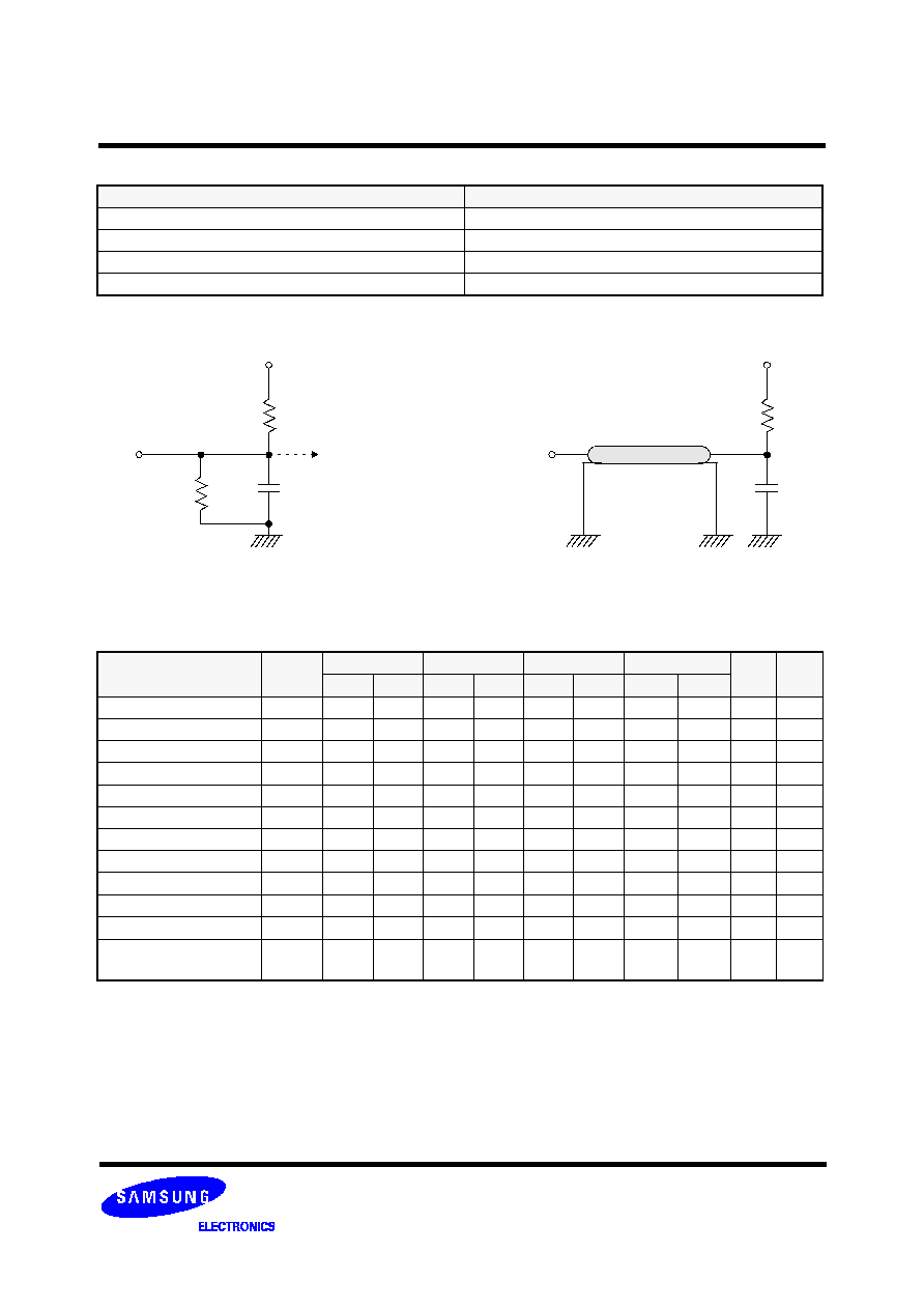
AC OPERATING TEST CONDITIONS
(T
A
= 0 to 70
∞
C, V
DD
= 3.3V
±
0.3V, unless otherwise noted.)
Note : If CLK transition time is longer than 1ns, timing parameters should be compensated. Add [(tr+tf)/2-1]ns for transition time longer than 1ns. Transi-
tion time is measured between V
IL
(Max) and V
IH
(Min).
Parameter
Value
Timing Reference Levels of Input/Output Signals
1.4V
Input Signal Levels
V
IH
/V
IL
=2.4V/0.4V
Transition Time (Rise & Fall) of Input Signals
tr/tf=1ns/1ns
Output Load
LVTTL
3.3V
1200
870
Output
50pF
V
OH
(DC)=2.4V, I
OH
=-2mA
V
OL
(DC)=0.4V, I
OL
=2mA
Vtt=1.4V
50
Output
50pF
Z
0
=50
(Fig. 2) AC Output Load Circuit
(Fig. 1) DC Output Load Circuit
(AC operating conditions unless otherwise noted)
Note :
1. These t
RC
values are for BL=8. For BL=4, t
RC
=6 clks for up to 100MHz, t
RC
=6 clks for up to 83MHz, t
RC
=4 clks for up to 66MHz, t
RC
=4 clks for up to
50MHz, and t
RC
=3 clks for up to 33MHz.
RAS latency increase means, a simultaneous t
RC
increase in the same number of cycles.
( If RAS latency is 3 clks, t
RC
is 12 clks for BL=8.) Refer to attached technical note for gapless operation.
2. These
t
VCVC
values are for BL=8. For BL=4,
t
VCVC
=4clks for up to 100MHz,
t
VCVC
=4clks for up to 83MHz,
t
VCVC
=3clks for up to 66MHz,
t
VCVC
=3clks for
up to 50MHz, and
t
VCVC
=2clks for up to 33MHz.
Refer to attached technical note for gapless operation.
Parameter
Symbol
up to 100MHz
up to 83MHz
up to 66MHz
up to 50 Mhz
Unit
Notes
Min
Max
Min
Max
Min
Max
Min
Max
CLK Cycle Time
t
CC
10
12
15
-
20
-
ns
CLK to Valid Output Delay
t
SAC
-
6
-
6
-
6
-
6
ns
Data Output Hold Time
t
OH
2
-
2
-
2
-
2
-
ns
CLK High Pulse Width
t
CH
3
-
3.5
-
4
-
6.5
-
ns
CLK Low Pulse Width
t
CL
3
-
3.5
-
4
-
6.5
-
ns
Row-active to Row-active
t
RC
10
-
10
-
8
-
8
-
clks
1
Input Setup Time
t
SS
2
-
3
-
4
-
4
-
ns
Input Hold Time
t
SH
1
-
1
-
2
-
2
-
ns
CLK to Output in Low-Z
t
SLZ
0
-
0
-
0
-
0
-
ns
CLK to Output in High-Z
t
SHZ
-
7
-
8
-
10
-
15
ns
Transition Time
t
T
0.1
10
0.1
10
0.1
10
0.1
10
ns
Valid CAS Enable to Valid
CAS Enable
t
VCVC
8
-
8
-
7
-
7
-
clks
2
OPERATING AC PARAMETERS