128M DDR SDRAM
K4D263238F
- 3 -
Rev 1.1 (May 2003)
The K4D263238F is 134,217,728 bits of hyper synchronous data rate Dynamic RAM organized as 4 x 1,048,576 words by
32 bits, fabricated with SAMSUNG
s high performance CMOS technology. Synchronous features with Data Strobe allow
extremely high performance up to
2.0GB/s/chip.
I/O transactions are possible on both edges of the clock cycle. Range of
operating frequencies, programmable burst length and programmable latencies allow the device to be useful for a variety
of high performance memory system applications.
∑ 2.5V ± 5% power supply for device operation
∑ 2.5V ± 5% power supply for I/O interface
∑ SSTL_2 compatible inputs/outputs
∑ 4 banks operation
∑ MRS cycle with address key programs
-. Read latency 3 (clock)
-. Burst length (2, 4, 8 and Full page)
-. Burst type (sequential & interleave)
∑ Full page burst length for sequential burst type only
∑ Start address of the full page burst should be even
∑ All inputs except data & DM are sampled at the positive
going edge of the system clock
∑ Differential clock input
∑ No Write Interrupted by Read function
GENERAL DESCRIPTION
FEATURES
∑ Data I/O transactions on both edges of Data strobe
∑ DLL aligns DQ and DQS transitions with Clock transition
∑ Edge aligned data & data strobe output
∑ Center aligned data & data strobe input
∑ DM for write masking only
∑ Auto & Self refresh
∑ 32ms refresh period (4K cycle)
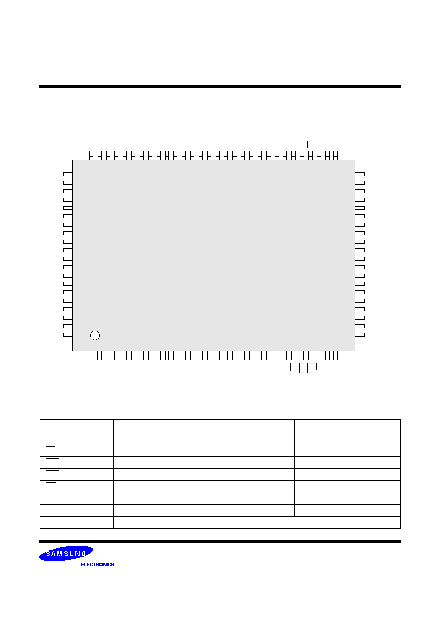
∑ 100pin TQFP package
∑ Maximum clock frequency up to 250MHz
∑ Maximum data rate up to 500Mbps/pin
FOR 1M x 32Bit x 4 Bank DDR SDRAM
1M x 32Bit x 4 Banks Double Data Rate Synchronous DRAM
with Bi-directional Data Strobe and DLL
ORDERING INFORMATION
K4D263238F-UC is the Lead Free package part number.
Part NO.
Max Freq.
Max Data Rate
Interface
Package
K4D263238F-QC40
250MHz
500Mbps/pin
SSTL_2
100 TQFP
K4D263238F-QC50
200MHz
400Mbps/pin
128M DDR SDRAM
K4D263238F
- 5 -
Rev 1.1 (May 2003)
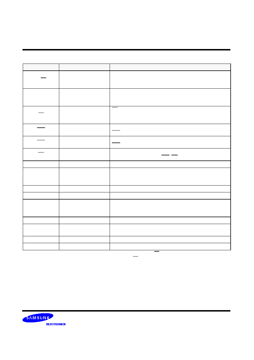
INPUT/OUTPUT FUNCTIONAL DESCRIPTION
*1 : The timing reference point for the differential clocking is the cross point of CK and CK.
For any applications using the single ended clocking, apply V
REF
to CK pin.
Symbol
Type
Function
CK, CK
*1
Input
The differential system clock Input.
All of the inputs are sampled on the rising edge of the clock except
DQ
s and DM
s that are sampled on both edges of the DQS.
CKE
Input
Activates the CK signal when high and deactivates the CK signal
when low. By deactivating the clock, CKE low indicates the Power
down mode or Self refresh mode.
CS
Input
CS enables the command decoder when low and disabled the com-
mand decoder when high. When the command decoder is disabled,
new commands are ignored but previous operations continue.
RAS
Input
Latches row addresses on the positive going edge of the CK with
RAS low. Enables row access & precharge.
CAS
Input
Latches column addresses on the positive going edge of the CK with
CAS low. Enables column access.
WE
Input
Enables write operation and row precharge.
Latches data in starting from CAS, WE active.
DQS
Input/Output
Data input and output are synchronized with both edge of DQS.
DM
0
~ DM
3
Input
Data In mask. Data In is masked by DM Latency=0 when DM is high
in burst write. DM
0
for DQ
0
~ DQ
7,
DM
1
for DQ
8
~ DQ
15,
DM
2
for
DQ
16
~ DQ
23,
DM
3
for DQ
24
~ DQ
31.
DQ
0
~ DQ
31
Input/Output
Data inputs/Outputs are multiplexed on the same pins.
BA
0
, BA
1
Input
Selects which bank is to be active.
A
0
~ A
11
Input
Row/Column addresses are multiplexed on the same pins.
Row addresses : RA
0
~ RA
11
, Column addresses : CA
0
~ CA
7
.
Column address CA
8
is used for auto precharge.
V
DD
/V
SS
Power Supply
Power and ground for the input buffers and core logic.
V
DDQ
/V
SSQ
Power Supply
Isolated power supply and ground for the output buffers to provide
improved noise immunity.
V
REF
Power Supply
Reference voltage for inputs, used for SSTL interface.
MCL
Must Connect Low
Must connect Low