128M GDDR SDRAM
K4D263238G-GC
- 1 -
Rev 1.8 (March. 2005)
128Mbit GDDR SDRAM
Revision 1.8
March 2005
Samsung Electronics reserves the right to change products or specification without notice.
INFORMATION IN THIS DOCUMENT IS PROVIDED IN RELATION TO SAMSUNG PRODUCTS,
AND IS SUBJECT TO CHANGE WITHOUT NOTICE.
NOTHING IN THIS DOCUMENT SHALL BE CONSTRUED AS GRANTING ANY LICENSE,
EXPRESS OR IMPLIED, BY ESTOPPEL OR OTHERWISE,
TO ANY INTELLECTUAL PROPERTY RIGHTS IN SAMSUNG PRODUCTS OR TECHNOLOGY. ALL
INFORMATION IN THIS DOCUMENT IS PROVIDED
ON AS "AS IS" BASIS WITHOUT GUARANTEE OR WARRANTY OF ANY KIND.
1. For updates or additional information about Samsung products, contact your nearest Samsung office.
2. Samsung products are not intended for use in life support, critical care, medical, safety equipment, or similar
applications where Product failure could result in loss of life or personal or physical harm, or any military or
defense application, or any governmental procurement to which special terms or provisions may apply.
128M GDDR SDRAM
K4D263238G-GC
- 2 -
Rev 1.8 (March. 2005)
Revision History
Revision 1.8 (March 5, 2005)
� Remove 80% and 120% of the IBIS(I - V) curve in the data sheet
Revision 1.7 (February 5, 2005)
� Changed EMRS table for Driver Impedance control .
� Added IBIS (I - V) curve in the data sheet
Revision 1.6 (January 5, 2005)
� Added 200MHz/ 166MHz AC characteristics in AC CHARACTERISTICS (II) table of K4D263238G-VC2A and
K4D263238G-VC33.
� Typo corrected
Revision 1.5 (December 29, 2004)
� Added tCK(min)=5ns @ CL3
� Changed tCK(max) of K4D263238G-GC2A from 4ns to 10ns
Revision 1.4 (November 30, 2004)
� Typo Corrected in DC table
Revision 1.3 (November 12, 2004)
� Changed AC spec format
� Changed DC spec measurement condition from VDD(typ) to VDD(max)
Revision 1.2 (October 18, 2004)
� Changed unit of tWR and tWR_A from ns to tCK to avoid misuse.
� Added lower speed timing set
Revision 1.1 (August 31, 2004)
� Added 100% driver strength option as A6A1="11"
Revision 1.0 (July 12, 2004)
� Defined DC spec
Revision 0.4 (June 20, 2004)
� Removed K4D26323QG-GC40/45 from the spec
� Added dummy cycle (20tCK) between EMRS and MRS during the power-up sequence.
Revision 0.3 (June 8, 2004)
� Internal only
Revision 0.2 (April 22, 2004)
� Changed CAS latency of K4D263238G-GC2A from 4tCK to 5tCK
� Changed tWR & tWR_A of K4D263238G-GC2A from 4tCK to 5tCK

128M GDDR SDRAM
K4D263238G-GC
- 3 -
Rev 1.8 (March. 2005)
Revision History
Revision 0.1 (April 19, 2004)
� Changed tRCDRD of K4D263238G-GC33/36 from 4tCK to 5tCK
� Changed tRCDWR of K4D263238G-GC33/36 from 2tCK to 3tCK
� Changed tWR of K4D263238G-GC2A/33/36 from 3tCK to 4tCK.
� Changed tDAL of K4D263238G-GC2A from 8tCK to 9tCK
� Changed tDAL of K4D263238G-GC33/36 from 7tCK to 8tCK
Revision 0.0 (April 7, 2004)
- Target spec
� Defined Target specification
128M GDDR SDRAM
K4D263238G-GC
- 4 -
Rev 1.8 (March. 2005)
The K4D263238G is 134,217,728 bits of hyper synchronous data rate Dynamic RAM organized as 4 x1,048,576 words by
32 bits, fabricated with SAMSUNG
'
s high performance CMOS technology. Synchronous features with Data Strobe allow
extremely high performance up to 2.8GB/s/chip. I/O transactions are possible on both edges of the clock cycle. Range of
operating frequencies, programmable burst length and programmable latencies allow the device to be useful for a variety
of high performance memory system applications.
� 2.5V � 5% power supply for device operation
� 2.5V � 5% power supply for I/O interface
� SSTL_2 compatible inputs/outputs
� 4 banks operation
� MRS cycle with address key programs
-. Read latency 3, 4 (clock)
-. Burst length (2, 4 and 8)
-. Burst type (sequential & interleave)
� All inputs except data & DM are sampled at the positive
going edge of the system clock
� Differential clock input
GENERAL DESCRIPTION
FEATURES
� No Wrtie-Interrupted by Read Function
� 4 DQS's ( 1DQS / Byte )
� Data I/O transactions on both edges of Data strobe
� DLL aligns DQ and DQS transitions with Clock transition
� Edge aligned data & data strobe output
� Center aligned data & data strobe input
� DM for write masking only
� Auto & Self refresh
� 32ms refresh period (4K cycle)
� 144-Ball FBGA
� Maximum clock frequency up to 350MHz
� Maximum data rate up to 700Mbps/pin
FOR 1M x 32Bit x 4 Bank DDR SDRAM
1M x 32Bit x 4 Banks Graphic Double Data Rate Synchronous DRAM
with Bi-directional Data Strobe and DLL
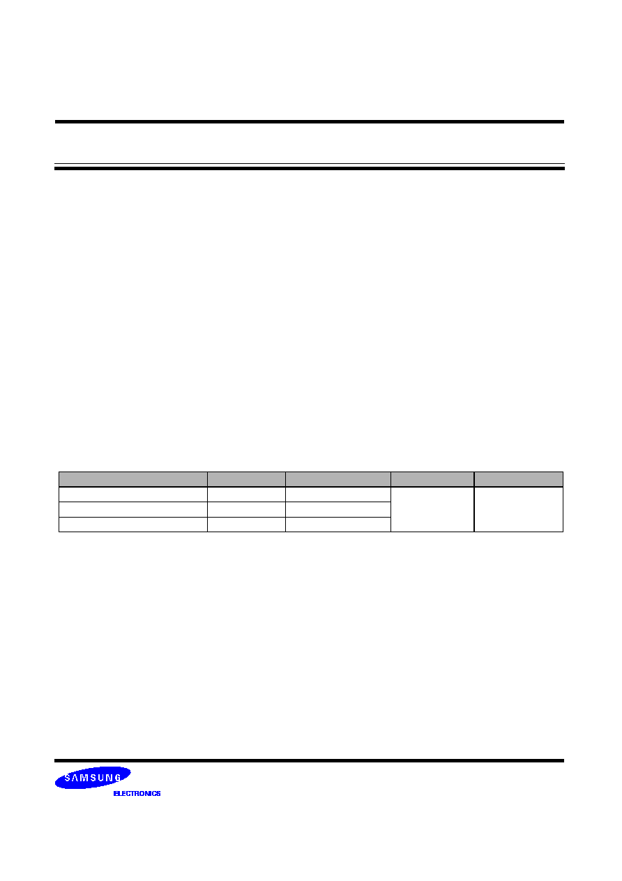
ORDERING INFORMATION
K4D263238G-VC is the Lead Free package part number.
Part NO.
Max Freq.
Max Data Rate
Interface
Package
K4D263238G-GC2A
350MHz
700Mbps/pin
SSTL_2
144-Ball FBGA
K4D263238G-GC33
300MHz
600Mbps/pin
K4D263238G-GC36
275MHz
550Mbps/pin
128M GDDR SDRAM
K4D263238G-GC
- 5 -
Rev 1.8 (March. 2005)
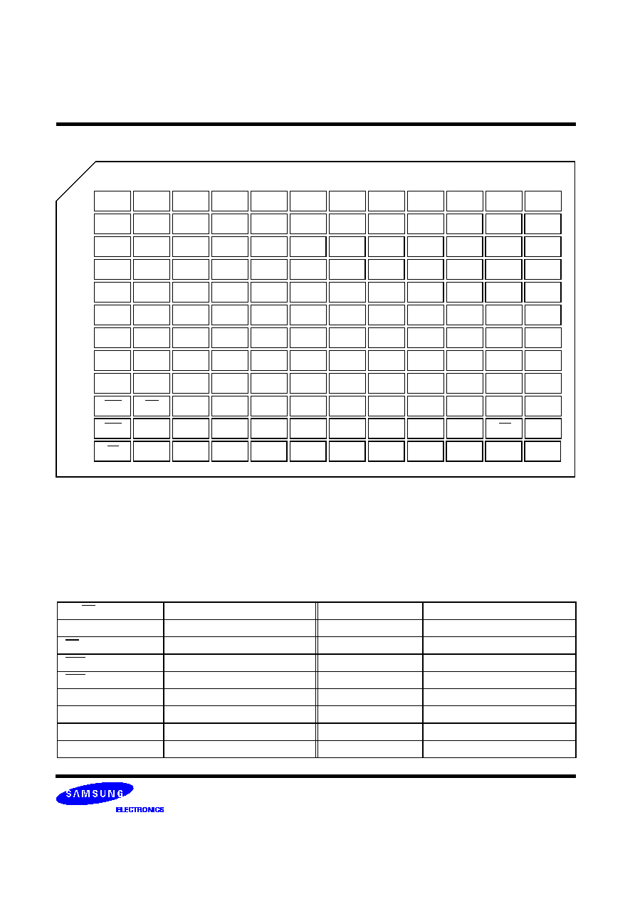
PIN CONFIGURATION
(Top View)
PIN DESCRIPTION
CK,CK
Differential Clock Input
BA
0
, BA
1
Bank Select Address
CKE
Clock Enable
A
0
~A
11
Address Input
CS
Chip Select
DQ
0
~ DQ
31
Data Input/Output
RAS
Row Address Strobe
V
DD
Power
CAS
Column Address Strobe
V
SS
Ground
WE
Write Enable
V
DDQ
Power for DQ
'
s
DQS
Data Strobe
V
SSQ
Ground for DQ
'
s
DM
Data Mask
NC
No Connection
RFU
Reserved for Future Use
MCL
Must Connect Low
DQS0
VSS
RFU
1
Thermal
VSS
Thermal
VSS
Thermal
VSS
Thermal
VSS
Thermal
VSS
Thermal
VSS
Thermal
VSS
Thermal
VSS
Thermal
VSS
Thermal
VSS
Thermal
VSS
Thermal
VSS
Thermal
VSS
Thermal
VSS
Thermal
VSS
Thermal
VSSQ
VSSQ
VSSQ
VSSQ
VSSQ
VSSQ
VSSQ
VSSQ
VSSQ
VSSQ
VSSQ
VSSQ
VSSQ
VSSQ
VSSQ
VSSQ
VSSQ
VSSQ
VSSQ
VSSQ
VSS
VSS
VSS
VSS
VSS
VSS
VSS
VSS
VSS
RFU
2
A5
A6
DQ4
DQ6
DQ7
DQ17
DQ19
DQS2
DQ21
DQ22
CAS
RAS
CS
DM0
VDDQ
DQ5
VDDQ
DQ16
DQ18
DM2
DQ20
DQ23
WE
NC
NC
NC
VDD
VDDQ
VDDQ
NC
VDDQ
VDDQ
VDD
NC
BA0
BA1
A0
DQ3
VDDQ
DQ31
DQ1
A10
A2
A1
VDD
VDD
VDD
DQ2
VDDQ
VDD
A11
A3
A9
A4
DQ0
VDDQ
VDD
DQ29
DQ30
DQ28
VDDQ
NC
VSS
A7
VDDQ
VDDQ
NC
VDDQ
VDDQ
VDD
CK
A8/AP
DM3
VDDQ
DQ26
VDDQ
DQ15
DQ13
DM1
DQ11
DQ9
NC
CK
CKE
DQS3
DQ27
DQ25
DQ24
DQ14
DQ12
DQS1
DQ10
DQ8
NC
VREF
2
3
4
5
6
7
8
9
10
11
12
13
B
C
D
E
F
G
H
J
K
L
M
N
NOTE:
1. RFU1 is reserved for A12
2. RFU2 is reserved for BA2
3. VSS Thermal balls are optional
MCL