
256M GDDR SDRAM
K4D551638F-TC
- 1 -
Rev 1.7 (June 2004)
Target Spec
256Mbit GDDR SDRAM
Revision 1.7
June 2004
4M x 16Bit x 4 Banks
Graphic Double Data Rate
Samsung Electronics reserves the right to change products or specification without notice.
Synchronous DRAM
256M GDDR SDRAM
K4D551638F-TC
- 2 -
Rev 1.7 (June 2004)
Target Spec
Revision History
Revision 1.7 (June 15, 2004) -
Target Spec
∑ Changed VDD/VDDQ of K4D551638F-TC33 from 2.8V + 0.1V to 2.8V(min)/2.95V(max)
Revision 1.6 (March 31, 2004) -
Target Spec
∑ AC Changes : Refer to the AC characteristics of page 13 and 14.
Revision 1.5 (March 18, 2004) -
Target Spec
∑ Added K4D551638F-TC33 in the data sheet.
Revision 1.4 (February 27, 2004) -
Target Spec
∑ Added K4D551638F-TC36/40 in the data sheet.
Revision 1.3 (December 5, 2003)
∑ Changed VDD/VDDQ of K4D551638F-TC50 from 2.5V + 5% to 2.6V + 0.1V
Revision 1.2 (November 11, 2003)
∑ "Wrtie-Interrupted by Read Function" is supported
Revision 1.1 (October 13, 2003)
∑ Defined ICC7 value
Revision 1.0 (October 10, 2003)
∑ Defined DC spec
∑ Changed part number of 16Mx16 GDDR F-die from K4D561638F-TC to K4D551638F-TC.
Revision 0.1 (October 2, 2003) -
Target Spec
∑ Added Lead free package part number in the data sheet.
∑ Removed K4D561638F-TC40 from the data sheet.
Revision 0.0 (July 2, 2003) -
Target Spec
∑ Defined Target Specification

256M GDDR SDRAM
K4D551638F-TC
- 3 -
Rev 1.7 (June 2004)
Target Spec
The K4D551638F is 268,435,456 bits of hyper synchronous data rate Dynamic RAM organized as 4 x 4,194,304 words by
16 bits, fabricated with SAMSUNG
'
s high performance CMOS technology. Synchronous features with Data Strobe allow
extremely high performance up to 1.1GB/s/chip. I/O transactions are possible on both edges of the clock cycle. Range of
operating frequencies, programmable burst length and programmable latencies allow the device to be useful for a variety
of high performance memory system applications.
GENERAL DESCRIPTION
FEATURES
FOR 4M x 16Bit x 4 Bank GDDR SDRAM
4M x 16Bit x 4 Banks Graphic Double Data Rate Synchronous DRAM
with Bi-directional Data Strobe and DLL
ORDERING INFORMATION
1. K4D551638F-LC is the Lead Free package part number.
2. For the K4D551638F-TC60, VDD & VDDQ = 2.5V + 5%
3. For the K4D551638F-TC36, VDD & VDDQ = 2.8V + 0.1V
4. For the K4D551638F-TC33, VDD & VDDQ = 2.8V ~ 2.95V
Part NO.
Max Freq.
Max Data Rate
Interface
Package
K4D551638F-TC33
300MHz
600Mbps/pin
SSTL_2
66pin TSOP-II
K4D551638F-TC36
275MHz
550Mbps/pin
K4D551638F-TC40
250MHz
500Mbps/pin
K4D551638F-TC50
200MHz
400Mbps/pin
K4D551638F-TC60*
166MHz
333Mbps/pin
∑ 2.6V + 0.1V power supply for device operation
∑ 2.6V + 0.1V power supply for I/O interface
∑ SSTL_2 compatible inputs/outputs
∑ 4 banks operation
∑ MRS cycle with address key programs
-. Read latency 3 (clock)
-. Burst length (2, 4 and 8)
-. Burst type (sequential & interleave)
∑ All inputs except data & DM are sampled at the positive
going edge of the system clock
∑ Differential clock input
∑ No Write-Interrupted by Read Function
∑ 2 DQS's ( 1DQS / Byte )
∑ Data I/O transactions on both edges of Data strobe
∑ DLL aligns DQ and DQS transitions with Clock transition
∑ Edge aligned data & data strobe output
∑ Center aligned data & data strobe input
∑ DM for write masking only
∑ Auto & Self refresh
∑ 64ms refresh period (8K cycle)
∑ 66pin TSOP-II
∑ Maximum clock frequency up to 300MHz
∑ Maximum data rate up to 600Mbps/pin
256M GDDR SDRAM
K4D551638F-TC
- 4 -
Rev 1.7 (June 2004)
Target Spec
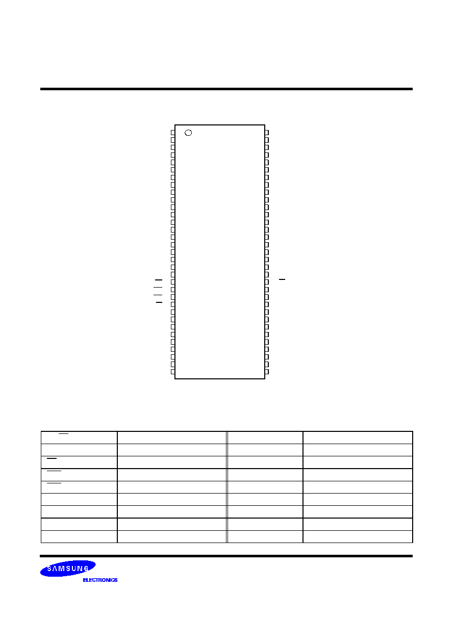
PIN CONFIGURATION
(Top View)
PIN DESCRIPTION
CK,CK
Differential Clock Input
BA
0
, BA
1
Bank Select Address
CKE
Clock Enable
A
0
~A
12
Address Input
CS
Chip Select
DQ
0
~ DQ
15
Data Input/Output
RAS
Row Address Strobe
V
DD
Power
CAS
Column Address Strobe
V
SS
Ground
WE
Write Enable
V
DDQ
Power for DQ
'
s
L(U)DQS
Data Strobe
V
SSQ
Ground for DQ
'
s
L(U)DM
Data Mask
NC
No Connection
RFU
Reserved for Future Use
VREF
Reference voltage
1
66 PIN TSOP(II)
(400mil x 875mil)
2
3
4
5
6
7
8
9
10
11
12
20
19
18
17
16
15
14
13
27
26
25
24
23
22
21
54
53
52
51
50
49
48
47
46
45
44
43
35
36
37
38
39
40
41
42
55
56
57
58
59
60
34
(0.65 mm Pin Pitch)
33
32
31
30
29
28
61
62
63
64
65
66
V
DD
DQ
0
V
DDQ
DQ
1
DQ
2
V
SSQ
DQ
3
DQ
4
V
DDQ
DQ
5
DQ
6
V
SSQ
BA
0
CS
RAS
CAS
WE
LDM
V
DDQ
DQ
7
V
DD
A
3
A
2
A
1
A
0
AP/A
10
BA
1
NC
LDQS
NC
NC
NC
V
DD
V
SS
DQ
15
V
SSQ
DQ
14
DQ
13
V
DDQ
DQ
12
DQ
11
V
SSQ
DQ
10
DQ
9
V
DDQ
A
11
CKE
CK
UDM
V
REF
V
SSQ
DQ
8
V
SS
A
4
A
5
A
6
A
7
A
8
A
9
NC
UDQS
NC
V
SS
CK
NC
A
12
256M GDDR SDRAM
K4D551638F-TC
- 5 -
Rev 1.7 (June 2004)
Target Spec
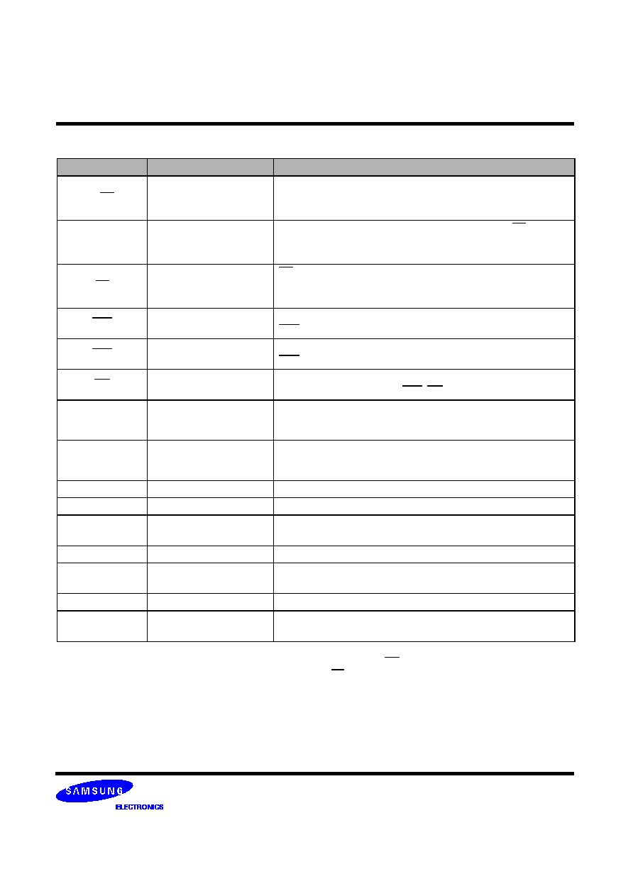
INPUT/OUTPUT FUNCTIONAL DESCRIPTION
*1 : The timing reference point for the differential clocking is the cross point of CK and CK.
For any applications using the single ended clocking, apply V
REF
to CK pin.
Symbol
Type
Function
CK, CK*1
Input
The differential system clock Input.
All of the inputs are sampled on the rising edge of the clock except
DQ
'
s and DM
'
s that are sampled on both edges of the DQS.
CKE
Input
Activates the CK signal when high and deactivates the CK signal
when low. By deactivating the clock, CKE low indicates the Power
down mode or Self refresh mode.
CS
Input
CS enables the command decoder when low and disabled the com-
mand decoder when high. When the command decoder is disabled,
new commands are ignored but previous operations continue.
RAS
Input
Latches row addresses on the positive going edge of the CK with
RAS low. Enables row access & precharge.
CAS
Input
Latches column addresses on the positive going edge of the CK with
CAS low. Enables column access.
WE
Input
Enables write operation and row precharge.
Latches data in starting from CAS, WE active.
LDQS,UDQS
Input/Output
Data input and output are synchronized with both edge of DQS.
For the x16, LDQS corresponds to the data on DQ0-DQ7 ; UDQS
corresponds to the data on DQ8-DQ15.
LDM,UDM
Input
Data in Mask. Data In is masked by DM Latency=0 when DM is
high in burst write. For the x16, LDM corresponds to the data on
DQ0-DQ7 ; UDM correspons to the data on DQ8-DQ15.
DQ
0
~ DQ
15
Input/Output
Data inputs/Outputs are multiplexed on the same pins.
BA
0
, BA
1
Input
Selects which bank is to be active.
A
0
~ A
12
Input
Row/Column addresses are multiplexed on the same pins.
Row addresses : RA
0
~ RA
12
, Column addresses : CA
0
~ CA
8
.
V
DD
/V
SS
Power Supply
Power and ground for the input buffers and core logic.
V
DDQ
/V
SSQ
Power Supply
Isolated power supply and ground for the output buffers to provide
improved noise immunity.
V
REF
Power Supply
Reference voltage for inputs, used for SSTL interface.
NC/RFU
No connection/
Reserved for future use
This pin is recommended to be left "No connection" on the device