256M GDDR SDRAM
K4D553235F-GC
- 1 -
Rev 1.6 (May 2005)
256Mbit GDDR SDRAM
Revision 1.6
March 2005
Samsung Electronics reserves the right to change products or specification without notice.
INFORMATION IN THIS DOCUMENT IS PROVIDED IN RELATION TO SAMSUNG PRODUCTS,
AND IS SUBJECT TO CHANGE WITHOUT NOTICE.
NOTHING IN THIS DOCUMENT SHALL BE CONSTRUED AS GRANTING ANY LICENSE,
EXPRESS OR IMPLIED, BY ESTOPPEL OR OTHERWISE,
TO ANY INTELLECTUAL PROPERTY RIGHTS IN SAMSUNG PRODUCTS OR TECHNOLOGY. ALL
INFORMATION IN THIS DOCUMENT IS PROVIDED
ON AS "AS IS" BASIS WITHOUT GUARANTEE OR WARRANTY OF ANY KIND.
1. For updates or additional information about Samsung products, contact your nearest Samsung office.
2. Samsung products are not intended for use in life support, critical care, medical, safety equipment, or similar
applications where Product failure could result in loss of life or personal or physical harm, or any military or
defense application, or any governmental procurement to which special terms or provisions may apply.

256M GDDR SDRAM
K4D553235F-GC
- 2 -
Rev 1.6 (May 2005)
Revision History
Revision 1.6 (May 26, 2005)
� Added CL3 of MRS table
Revision 1.5 (March 16, 2005)
� Corrected the spec revision history from 1.1 ~ 1.4 as below.
Revision 1.4 (March 10, 2005)
� Added a tCK(min) value for -GC33@CL=3
Revision 1.3 (March 04, 2005)
� Removed K4D553235F-GC22 from the datasheet
Revision 1.2 (February 03, 2005)
� Removed -GJ from the spec which is no longer valid.
� Added a couple of note below AC timing table.
Revision 1.1 (December 14, 2004)
� Removed K4D553235F-GC20 from the specification.
� Dualized the 400MHz part's part number by its operating voltage. Newly added -GJ25 operating voltage is equal to 2.0V(typical) which is in mass pro-
duction now. The 400MHz part with VDD & VDDQ= 1.8V(typical) which represented as -GC25 will be available by the 2nd quarter of '05
� Added a couple of note below AC timing table.
Revision 1.0 (September 21, 2004)
� Defined DC specification
Revision 0.1 (June 16, 2004) -
Target Spec
� Defined target specification
Revision 0.0 (May 07, 2004) -
Target Spec
� Defined target specification
256M GDDR SDRAM
K4D553235F-GC
- 3 -
Rev 1.6 (May 2005)
The K4D553235F is 268,435,456 bits of hyper synchronous data rate Dynamic RAM organized as 4 x 2,097,152 words by
32 bits, fabricated with SAMSUNG
'
s high performance CMOS technology. Synchronous features with Data Strobe allow
extremely high performance up to 3.6GB/s/chip. I/O transactions are possible on both edges of the clock cycle. Range of
operating frequencies, programmable burst length and programmable latencies allow the device to be useful for a variety
of high performance memory system applications.
� 1.8V � 0.1V power supply for device operation
� 1.8V � 0.1V power supply for I/O interface
� SSTL_18 compatible inputs/outputs
� 4 banks operation
� MRS cycle with address key programs
-. Read latency 4, 5 and 6 (clock)
-. Burst length (2, 4 and 8)
-. Burst type (sequential & interleave)
� All inputs except data & DM are sampled at the positive
going edge of the system clock
� Differential clock input
GENERAL DESCRIPTION
FEATURES
� No Wrtie-Interrupted by Read Function
� 4 DQS's ( 1DQS / Byte )
� Data I/O transactions on both edges of Data strobe
� DLL aligns DQ and DQS transitions with Clock transition
� Edge aligned data & data strobe output
� Center aligned data & data strobe input
� DM for write masking only
� Auto & Self refresh
� 32ms refresh period (4K cycle)
� 144-Ball FBGA
� Maximum clock frequency up to 450MHz
� Maximum data rate up to 900Mbps/pin
FOR 2M x 32Bit x 4 Bank DDR SDRAM
2M x 32Bit x 4 Banks Graphic Double Data Rate Synchronous DRAM
with Bi-directional Data Strobe and DLL
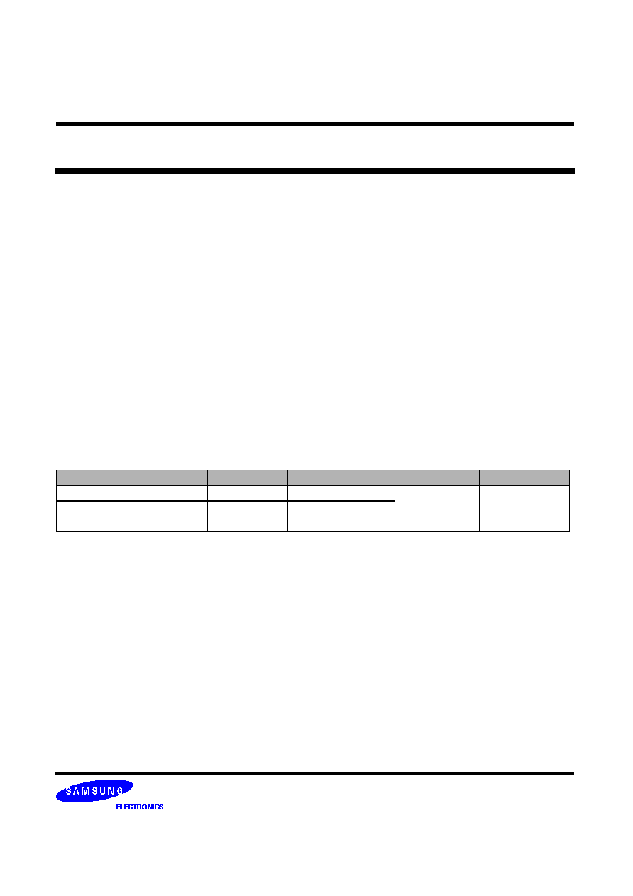
ORDERING INFORMATION
* K4D553235F-VC is the Lead Free package part number.
Part NO.
Max Freq.
Max Data Rate
Interface
Package
K4D553235F-GC25
400MHz
800Mbps/pin
SSTL_18
144-Ball FBGA
K4D553235F-GC2A
350MHz
700Mbps/pin
K4D553235F-GC33
300MHz
600Mbps/pin
256M GDDR SDRAM
K4D553235F-GC
- 4 -
Rev 1.6 (May 2005)
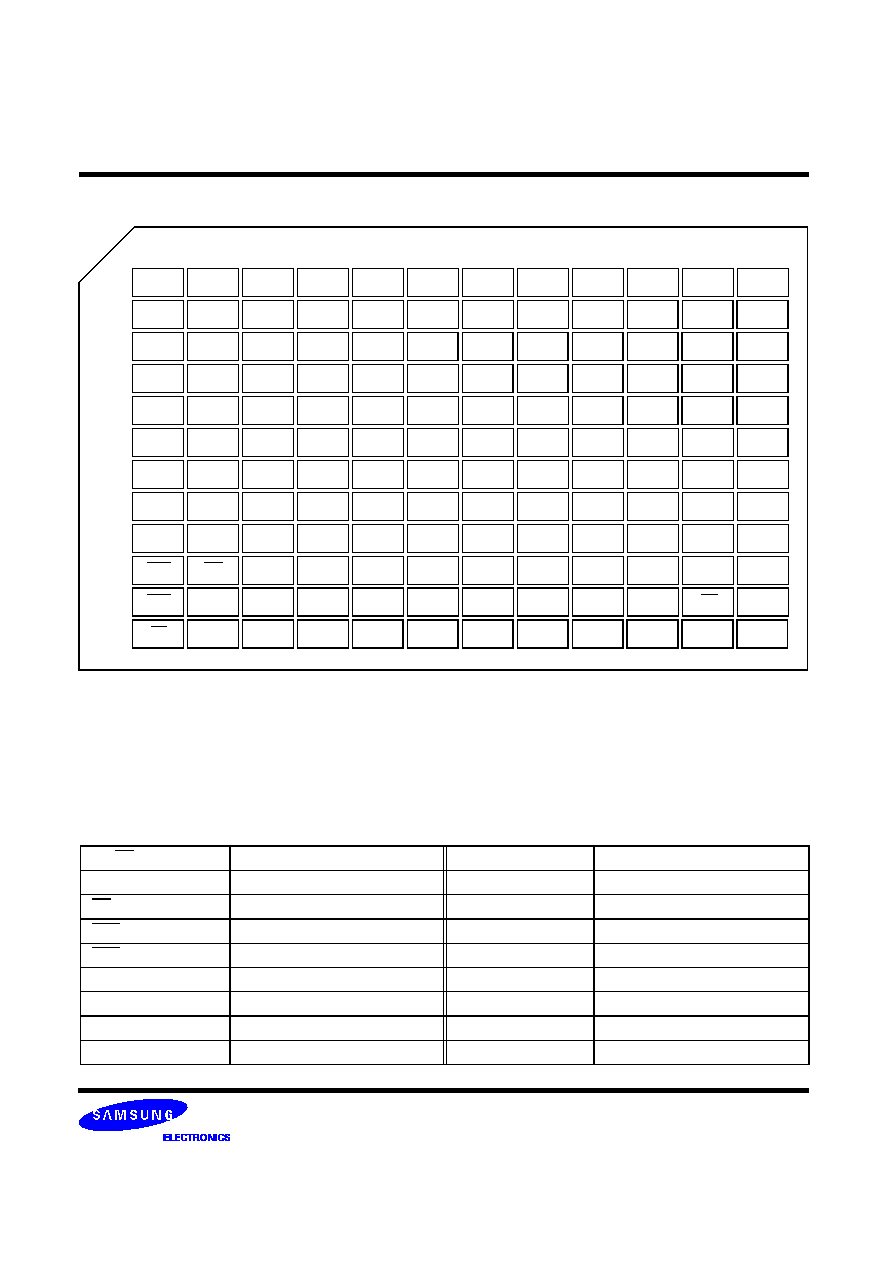
PIN CONFIGURATION
(Top View)
PIN DESCRIPTION
CK,CK
Differential Clock Input
BA
0
, BA
1
Bank Select Address
CKE
Clock Enable
A
0
~A
11
Address Input
CS
Chip Select
DQ
0
~ DQ
31
Data Input/Output
RAS
Row Address Strobe
V
DD
Power
CAS
Column Address Strobe
V
SS
Ground
WE
Write Enable
V
DDQ
Power for DQ
'
s
DQS
Data Strobe
V
SSQ
Ground for DQ
'
s
DM
Data Mask
NC
No Connection
RFU
Reserved for Future Use
MCL
Must Connect Low
DQS0
VSS
RFU
1
Thermal
VSS
Thermal
VSS
Thermal
VSS
Thermal
VSS
Thermal
VSS
Thermal
VSS
Thermal
VSS
Thermal
VSS
Thermal
VSS
Thermal
VSS
Thermal
VSS
Thermal
VSS
Thermal
VSS
Thermal
VSS
Thermal
VSS
Thermal
VSSQ
VSSQ
VSSQ
VSSQ
VSSQ
VSSQ
VSSQ
VSSQ
VSSQ
VSSQ
VSSQ
VSSQ
VSSQ
VSSQ
VSSQ
VSSQ
VSSQ
VSSQ
VSSQ
VSSQ
VSS
VSS
VSS
VSS
VSS
VSS
VSS
VSS
VSS
RFU
2
A5
A6
DQ4
DQ6
DQ7
DQ17
DQ19
DQS2
DQ21
DQ22
CAS
RAS
CS
DM0
VDDQ
DQ5
VDDQ
DQ16
DQ18
DM2
DQ20
DQ23
WE
NC
NC
NC
VDD
VDDQ
VDDQ
NC
VDDQ
VDDQ
VDD
NC
BA0
BA1
A0
DQ3
VDDQ
DQ31
DQ1
A10
A2
A1
VDD
VDD
VDD
DQ2
VDDQ
VDD
A11
A3
A9
A4
DQ0
VDDQ
VDD
DQ29
DQ30
DQ28
VDDQ
NC
VSS
A7
VDDQ
VDDQ
NC
VDDQ
VDDQ
VDD
CK
A8/AP
DM3
VDDQ
DQ26
VDDQ
DQ15
DQ13
DM1
DQ11
DQ9
NC
CK
CKE
DQS3
DQ27
DQ25
DQ24
DQ14
DQ12
DQS1
DQ10
DQ8
NC
VREF
2
3
4
5
6
7
8
9
10
11
12
13
B
C
D
E
F
G
H
J
K
L
M
N
NOTE:
1. RFU1 is reserved for A12
2. RFU2 is reserved for BA2
3. VSS Thermal balls are optional
MCL
256M GDDR SDRAM
K4D553235F-GC
- 5 -
Rev 1.6 (May 2005)
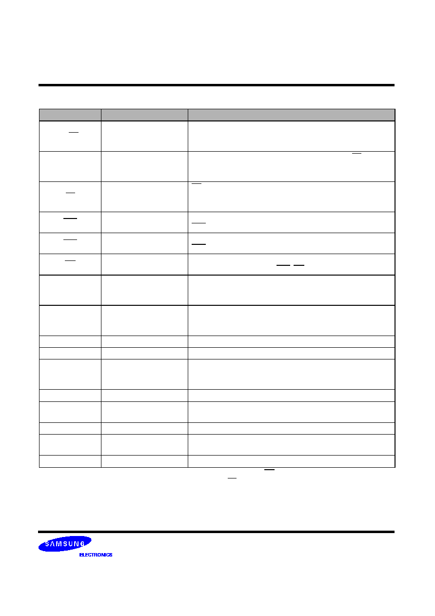
INPUT/OUTPUT FUNCTIONAL DESCRIPTION
*1 : The timing reference point for the differential clocking is the cross point of CK and CK.
For any applications using the single ended clocking, apply V
REF
to CK pin.
Symbol
Type
Function
CK, CK*1
Input
The differential system clock Input.
All of the inputs are sampled on the rising edge of the clock except
DQ
'
s and DM
'
s that are sampled on both edges of the DQS.
CKE
Input
Activates the CK signal when high and deactivates the CK signal
when low. By deactivating the clock, CKE low indicates the Power
down mode or Self refresh mode.
CS
Input
CS enables the command decoder when low and disabled the com-
mand decoder when high. When the command decoder is disabled,
new commands are ignored but previous operations continue.
RAS
Input
Latches row addresses on the positive going edge of the CK with
RAS low. Enables row access & precharge.
CAS
Input
Latches column addresses on the positive going edge of the CK with
CAS low. Enables column access.
WE
Input
Enables write operation and row precharge.
Latches data in starting from CAS, WE active.
DQS
0
~ DQS
3
Input/Output
Data input and output are synchronized with both edge of DQS.
DQS
0
for DQ
0
~ DQ
7,
DQS
1
for DQ
8
~ DQ
15,
DQS
2
for DQ
16
~ DQ
23,
DQS
3
for DQ
24
~ DQ
31.
DM
0
~ DM
3
Input
Data In mask. Data In is masked by DM Latency=0 when DM is high
in burst write. DM
0
for DQ
0
~ DQ
7,
DM
1
for DQ
8
~ DQ
15,
DM
2
for
DQ
16
~ DQ
23,
DM
3
for DQ
24
~ DQ
31.
DQ
0
~ DQ
31
Input/Output
Data inputs/Outputs are multiplexed on the same pins.
BA
0
, BA
1
Input
Selects which bank is to be active.
A
0
~ A
11
Input
Row/Column addresses are multiplexed on the same pins.
Row addresses : RA
0
~ RA
11
, Column addresses : CA
0
~ CA
7
, CA
9
Column address CA
8
is used for auto precharge.
V
DD
/V
SS
Power Supply
Power and ground for the input buffers and core logic.
V
DDQ
/V
SSQ
Power Supply
Isolated power supply and ground for the output buffers to provide
improved noise immunity.
V
REF
Power Supply
Reference voltage for inputs, used for SSTL interface.
NC/RFU
No connection/
Reserved for future use
This pin is recommended to be left "No connection" on the device
MCL
Must Connect Low
Must connect low