
Preliminary
64M DDR SGRAM
K4D623237M
The K4D623237 is 67,108,864 bits of hyper synchronous data rate Dynamic GRAM organized as 4 x 524,288 words by 32
bits, fabricated with SAMSUNG
s high performance CMOS technology. Synchronous features with Data Strobe allow
extremely high performance up to 1.328GB/s/chip. I/O transactions are possible on both edges of the clock cycle. Range of
operating frequencies, programmable burst length and programmable latencies allow the device to be useful for a variety
of high performance memory system applications.
∑ 3.3V
±
5% power supply for device operation
∑ 2.5V
±
5% power supply for I/O interface
∑ SSTL_2 compatible inputs/outputs
∑ 4 banks operation
∑ MRS cycle with address key programs
-. Read latency 2, 3 (clock)
-. Burst length (2, 4, 8 and Full page)
-. Burst type (sequential & interleave)
∑ Full page burst length for sequential burst type only
∑ Start address of the full page burst should be even
∑ All inputs except data & DM are sampled at the positive
going edge of the system clock
∑ Differential clock input
∑ Data I/O transactions on both edges of Data strobe
∑ Data input & output & DM are synchronized with DQS
GENERAL DESCRIPTION
FEATURES
∑ Edge aligned data & data strobe output
∑ Center aligned data & data strobe input
∑ DM for write masking only
∑ Auto & Self refresh
∑ 16ms refresh period (2K cycle)
∑ 100pin TQFP package
∑ Maximum clock frequency up to 166MHz
∑ Maximum data rate up to 333Mbps/pin
Graphics Features
∑ SMRS cycle.
-. Load color register
∑ 16 Columns Block Write.
∑ Byte Masking with DM for Block Write operation is sup-
ported.
FOR 512K x 32Bit x 4 Bank DDR SGRAM
512K x 32Bit x 4 Banks Double Data Rate Synchronous Graphic RAM
with Bi-directional Data Strobe
ORDERING INFORMATION
Part NO.
Max Freq.
Max Data Rate
Interface
Package
K4D623237M-QC60
166MHz
333Mbps/pin
SSTL_2
100 TQFP
K4D623237M-QC70
143MHz
286Mbps/pin
K4D623237M-QC80
125MHz
250Mbps/pin
K4D623237M-QC10
100MHz
200Mbps/pin
Preliminary
64M DDR SGRAM
K4D623237M
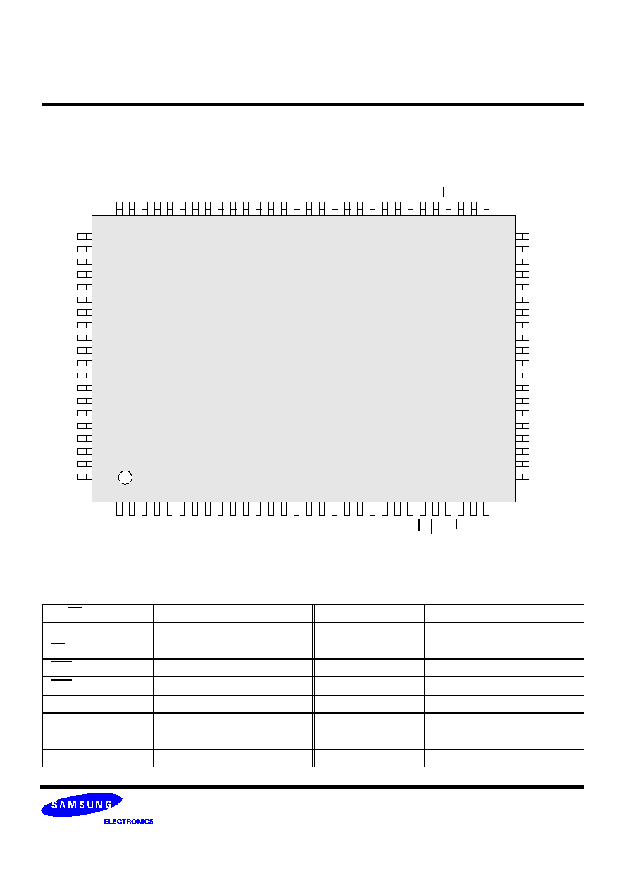
PIN CONFIGURATION
(Top View)
PIN DESCRIPTION
CK,CK
Differential Clock Input
BA
0
, BA
1
Bank Select Address
CKE
Clock Enable
A
0
~A
10
Address Input
CS
Chip Select
DQ
0
~ DQ
31
Data Input/Output
RAS
Row Address Strobe
V
DD
Power
CAS
Column Address Strobe
V
SS
Ground
WE
Write Enable
V
DDQ
Power for DQ
s
DQS
Data Strobe
V
SSQ
Ground for DQ
s
DMi
Data Mask
DSF
Define Special Function
RFU
Reserved for Future Use
MCL
Must Connect Low
DQ29
VSSQ
DQ30
DQ31
VSS
VDDQ
N.C
N.C
N.C
N.C
N.C
VSSQ
RFU
DQS
VDDQ
VDD
DQ0
DQ1
VSSQ
DQ2
81
82
83
84
85
86
87
88
89
90
91
92
93
94
95
96
97
98
99
100
D
Q
3
V
D
D
Q
D
Q
4
D
Q
5
V
S
S
Q
D
Q
6
D
Q
7
V
D
D
Q
D
Q
1
6
D
Q
1
7
V
S
S
Q
D
Q
1
8
D
Q
1
9
V
D
D
Q
V
D
D
V
S
S
D
Q
2
0
D
Q
2
1
V
S
S
Q
D
Q
2
2
D
Q
2
3
V
D
D
Q
D
M
0
D
M
2
W
E
C
A
S
R
A
S
C
S
B
A
0
B
A
1
1
2
3
4
5
6
7
8
9
1
0
1
1
1
2
1
3
1
4
1
5
1
6
1
7
1
8
1
9
2
0
2
1
2
2
2
3
2
4
2
5
2
6
2
7
2
8
2
9
3
0
A7
A6
A5
A4
VSS
A9
N.C
N.C
N.C
N.C
N.C
N.C
N.C
N.C
A10
VDD
A3
A2
A1
A0
50
49
48
47
46
45
44
43
42
41
40
39
38
37
36
35
34
33
32
31
100 Pin TQFP
20 x 14 mm
2
0.65mm pin Pitch
D
Q
2
8
V
D
D
Q
D
Q
2
7
D
Q
2
6
V
S
S
Q
D
Q
2
5
D
Q
2
4
V
D
D
Q
D
Q
1
5
D
Q
1
4
V
S
S
Q
D
Q
1
3
D
Q
1
2
V
D
D
Q
V
S
S
V
D
D
D
Q
1
1
D
Q
1
0
V
S
S
Q
D
Q
9
D
Q
8
V
D
D
Q
V
R
E
F
D
M
3
D
M
1
C
K
C
K
C
K
E
D
S
F
,
M
C
L
A
8
(
A
P
)
8
0
7
9
7
8
7
7
7
6
7
5
7
4
7
3
7
2
7
1
7
0
6
9
6
8
6
7
6
6
6
5
6
4
6
3
6
2
6
1
6
0
5
9
5
8
5
7
5
6
5
5
5
4
5
3
5
2
5
1
Preliminary
64M DDR SGRAM
K4D623237M
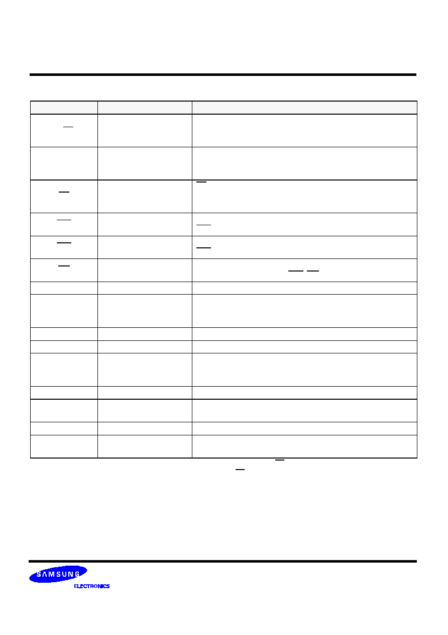
INPUT/OUTPUT FUNCTIONAL DESCRIPTION
*1 : The timing reference point for the differential clocking is the cross point of CK and CK.
For any applications using the single ended clocking, apply V
REF
to CK pin.
Symbol
Type
Function
CK, CK
*1
Input
The differential system clock Input.
All of the inputs are sampled on the rising edge of the clock except
DQ
s and DM
s that are sampled on both edges of the DQS.
CKE
Input
Activates the CK signal when high and deactivates the CK signal
when low. By deactivating the clock, CKE low indicates the Power
down mode or Self refresh mode.
CS
Input
CS enables the command decoder when low and disabled the com-
mand decoder when high. When the command decoder is disabled,
new commands are ignored but previous operations continue.
RAS
Input
Latches row addresses on the positive going edge of the CK with
RAS low. Enables row access & precharge.
CAS
Input
Latches column addresses on the positive going edge of the CK with
CAS low. Enables column access.
WE
Input
Enables write operation and row precharge.
Latches data in starting from CAS, WE active.
DQS
Input/Output
Data input and output are synchronized with both edge of DQS.
DM
0
~ DM
3
Input
Data In mask. Data In is masked by DM Latency=0 when DM is high
in burst write. DM
0
for DQ
0
~ DQ
7,
DM
1
for DQ
8
~ DQ
15,
DM
2
for
DQ
16
~ DQ
23,
DM
3
for DQ
24
~ DQ
31.
DQ
0
~ DQ
31
Input/Output
Data inputs/Outputs are multiplexed on the same pins.
BA
0
, BA
1
Input
Selects which bank is to be active.
A
0
~ A
10
Input
Row/Column addresses are multiplexed on the same pins.
Row addresses : RA
0
~ RA
10
, Column addresses : CA
0
~ CA
7
.
Column address CA
8
is used for auto precharge.
V
DD
/V
SS
Power Supply
Power and ground for the input buffers and core logic.
V
DDQ
/V
SSQ
Power Supply
Isolated power supply and ground for the output buffers to provide
improved noise immunity.
V
REF
Power Supply
Reference voltage for inputs, used for SSTL interface.
DSF, MCL
Define Special Function
Enables block write and special mode register set and must be con-
nected low to disable these special functions.
Preliminary
64M DDR SGRAM
K4D623237M
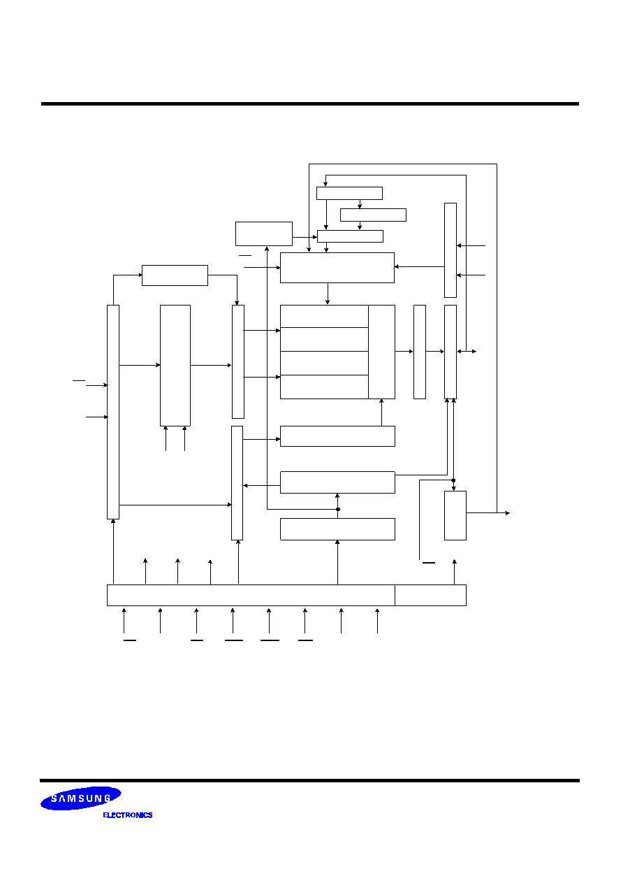
BLOCK DIAGRAM
(512Kbit x 32I/O x 4 Bank)
Bank Select
Timing Register
A
d
d
r
e
s
s
R
e
g
i
s
t
e
r
R
e
f
r
e
s
h
C
o
u
n
t
e
r
R
o
w
B
u
f
f
e
r
R
o
w
D
e
c
o
d
e
r
C
o
l
.
B
u
f
f
e
r
Data Input Register
Serial to parallel
512Kx32
512Kx32
512Kx32
512Kx32
S
e
n
s
e
A
M
P
2
-
b
i
t
p
r
e
f
e
t
c
h
O
u
t
p
u
t
B
u
f
f
e
r
I
/
O
C
o
n
t
r
o
l
Column Decoder
Latency & Burst Length
Programming Register
S
t
r
o
b
e
G
e
n
.
CK,CK
ADD
LCKE
CK,CK
CKE
CS
RAS
CAS
WE
DMi
LDMi
CK,CK
LCAS
LRAS
LCBR
LWE
LWCBR
L
R
A
S
L
C
B
R
CK, CK
64
64
32
32
LWE
LDMi
x32
DQi
Data Strobe
DSF
Intput Buffer
Color Register
MUX
Block Write
Control
Preliminary
64M DDR SGRAM
K4D623237M
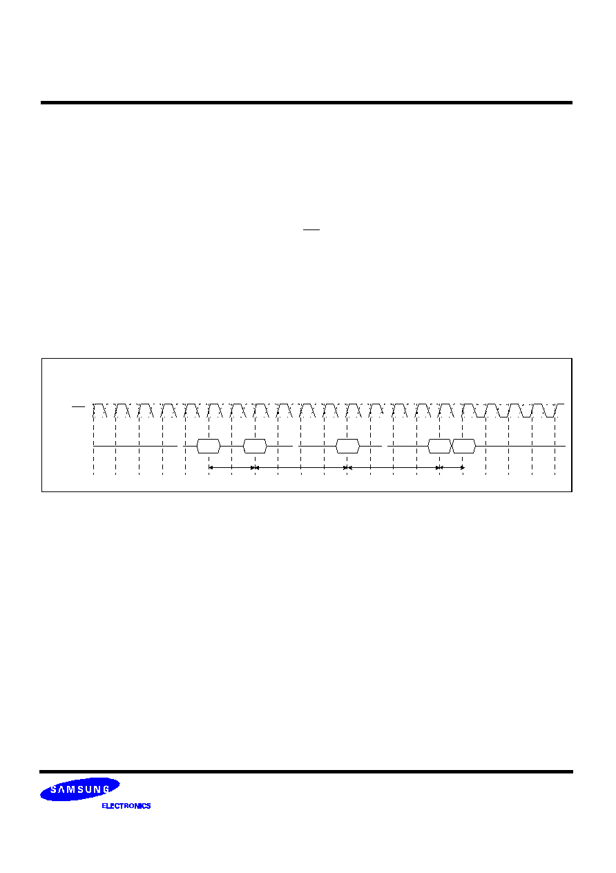
∑ Power-Up Sequence
DDR SGRAMs must be powered up and initialized in a predefined manner to prevent undefined operations.
1. Apply power and keep CKE at low state (All other inputs may be undefined)
- Apply VDD before VDDQ .
- Apply VDDQ before VREF & VTT
2. Start clock and maintain stable condition for a minimum of 200us.
3. The minimum of 200us after stable power and clock(CK,CK ), apply NOP and take CKE to be high .
4. Issue precharge command for all banks of the device.
5. Issue at least 2 or more auto-refresh commands.
6. Issue a mode register set command to initialize the mode register.
cf) Sequence of 4 & 5 is regardless of the order.
FUNCTIONAL DESCRIPTION
Power up Sequence & Auto Refresh(CBR)
Command
0
1
2
3
4
5
6
7
8
9
10
11
12
13
14
15
16
17
18
19
t
RP
Minimum of 2 Refresh Cycles are required
1 tck
precharge
ALL Bank
2nd Auto
Refresh
Mode
Register Set
Any
Command
t
RC
1st Auto
Refresh
t
RC
CK, CK
Inputs must be
stable for 200us
Preliminary
64M DDR SGRAM
K4D623237M
The mode register stores the data for controlling the various operating modes of DDR SGRAM. It programs CAS latency,
addressing mode, burst length, test mode and various vendor specific options to make DDR SGRAM useful for variety of
different applications. The default value of the mode register is not defined, therefore the mode register must be written
after power up to operate the DDR SGRAM. The mode register is written by asserting low on CS, RAS, CAS and WE(The
DDR SGRAM should be in active mode with CKE already high prior to writing into the mode register). The state of address
pins A
0
~ A
10
and BA
0
, BA
1
in the same cycle as CS, RAS, CAS and WE going low is written in the mode register. One
clock cycle is requested to complete the write operation in the mode register. The mode register contents can be changed
using the same command and clock cycle requirements during operation as long as all banks are in the idle state. The
mode register is divided into various fields depending on functionality. The burst length uses A
0
~ A
2
, addressing mode
uses A
3
, CAS latency(read latency from column address) uses A
4
~ A
6
. A
7
is used for test mode. A
7
, A
8
, BA
0
and BA
1
must be set to low for normal DDR SGRAM operation. Refer to the table for specific codes for various burst length,
addressing modes and CAS latencies.
MODE REGISTER SET(MRS)
Address Bus
Mode Register
CAS Latency
A
6
A
5
A
4
Latency
0
0
0
Reserve
0
0
1
Reserve
0
1
0
2
0
1
1
3
1
0
0
Reserve
1
0
1
Reserve
1
1
0
Reserve
1
1
1
Reserve
Burst Length
A
2
A
1
A
0
Burst Type
Sequential
Interleave
0
0
0
Reserve
Reserve
0
0
1
2
2
0
1
0
4
4
0
1
1
8
8
1
0
0
Reserve
Reserve
1
0
1
Reserve
Reserve
1
1
0
Reserve
Reserve
1
1
1
Full page
Reserve
A
7
mode
0
Normal
1
Test
Burst Type
A
3
Type
0
Sequential
1
Interleave
* RFU(Reserved for future use)
should stay "0" during MRS
cycle.
MRS Cycle
Command
*1 : MRS can be issued only at all banks precharge state.
*2 : Minimum
t
RP
is required to issue MRS command.
CK, CK
Precharge
NOP
NOP
MRS
NOP
NOP
NOP
2
0
1
5
3
4
8
6
7
Any
NOP
All Banks
Command
t
RP
t
MRD
=1 t
CK
BA
1
BA
0
A
10
A
9
A
8
A
7
A
6
A
5
A
4
A
3
A
2
A
1
A
0
RFU
TM
CAS Latency
BT
Burst Length

Preliminary
64M DDR SGRAM
K4D623237M
DEFINE SPECIAL FUNCTION(DSF)
The DSF controls the graphic applications of SGRAM. If DSF is tied to low, SGRAM functions are the same as SDRAM
functions. SGRAM can be used as an unified memory by the appropriate DSF command. All the graphic function mode
can be entered only by setting DSF high when issuing commands which otherwise would be normal SDRAM commands.
See the sessions below for the graphic functions that DSF control.
SPECIAL MODE REGISTER SET(SMRS)
There is a special mode register in DDR SGRAM. It is color register. This usage will be explained at "BLOCK WRITE"
session. When A6 and DSF goes high in the same cycle as CS, RAS, CAS and WE going low, load color register(LCR)
process is executed and the color register is filled with color data for associated DQ
s through the DQ pins. At the next
clock of LCR, a new commands can be issued. SMRS, compared with MRS, can be issued at the active state under the
condition that DQ
s are idle.
Special Mode Register Programmed with SMRS
Address
BA
1
BA
0
A
10
A
9
A
8
A
7
A
6
A
5
A
4
A
3
A
2
A
1
A
0
Function
X
LC
X
Load Color Register
A
6
Function
0
Disable
1
Enable
Command
SMRS Cycle
SMRS
NOP
NOP
NOP
NOP
NOP
NOP
DQS
DQ
s
Color
CK, CK
2
0
1
5
3
4
8
6
7
NOP
NOP
Load Color
Register
Block write is a feature allowing the simultaneous writing of consecutive 16 columns of data within a RAM device during
a single access cycle. During block write the data to be written comes from an internal "color" register. The block of col-
umn to be written is aligned on 16 column boundaries and is defined by the column address with the 4 LSB
s ignored.
Write command with DSF=High enables block write for the associated bank. A write command with DSF=Low enables
normal write for the associated bank. The block width is 16 column where column="n" bits for by "n" part. The color reg-
ister is the same width as the data port of the chip. The color register provides the data without column masking. So DQ
states are don
t cared. And Null Column Mask command with high state on DQs make no problem. DQS should toggle
once for valid data mask(DM) input. Block writes are always non-burst, independent of the burst length that has been
programmed into the mode register. Back to back block writes are allowed provided that the specified block write cycle
time(tBWC) is satisfied.
BLOCK WRITE
t
SMRD
=1 t
CK

Preliminary
64M DDR SGRAM
K4D623237M
t
CDLW=0
Note 2
1. t
CCD
: CAS to CAS delay. (=1 tCK)
2. t
CDLW
: Last data in to new column address delay. (=0 tCK)
3. t
BWC
: Block write minimum cycle time. (=1 tCK)
t
CDLW=0
Note 2
t
BWC
Note 3
2) Write interrupted by Block Write (BL=2)
3) Block Write to Block Write
CK, CK
CMD
ADD
CK, CK
CMD
ADD
DQ
*Note :
1) Block Write to Precharge
4) Byte Masking for Block Write
CK, CK
CMD
DMi
DQ
CK, CK
CMD
t
BPL
BW
PRE
WR
WR
WR
BW
t
CCD Note1
t
CCD Note1
A
B
C
D
BW
BW
A
B
SMRS
16 col.
BW
WRITE
16 col.
BW
Byte Masking
for Block Write
Byte Masking
for Normal Write
Color
2
0
1
5
3
4
8
6
7
2
0
1
5
3
4
8
6
7
2
0
1
5
3
4
8
6
7
2
0
1
5
3
4
8
6
7
DQS
Din 0
Din 1
Din A
0
Din A
1
Din B
0
Din B
1
Din C
0
Din C
1
t
BPL
PRE

Preliminary
64M DDR SGRAM
K4D623237M
Burst mode operation is used to provide a constant flow of data to memory locations(write cycle), or from memory loca-
tions(read cycle). There are two parameters that define how the burst mode operates. These parameters including burst
sequence and burst length are programmable and determined by address bits A
0
~ A
3
during the Mode Register Set com-
mand. The burst type is used to define the sequence in which the burst data will be delivered or stored to the SGRAM.
Two types of burst sequences are supported, sequential and interleaved. See the below table. The burst length controls
the number of bits that will be output after a read command, or the number of bits to be input after a write command. The
burst length can be programmed to have values of 2, 4, 8 or Full page. For the full page operation, the starting address
must be an even number.
BURST MODE OPERATION
BURST LENGTH AND SEQUENCE
Burst Length
Starting Address(A
2
, A
1
, A
0
)
Sequential Mode
Interleave Mode
2
xx0
0, 1
0, 1
xx1
1, 0
1, 0
4
x00
0, 1, 2, 3
0, 1, 2, 3
x01
1, 2, 3, 0
1, 0, 3, 2
x10
2, 3, 0, 1
2, 3, 0, 1
x11
3, 0, 1, 2
3, 2, 1, 0
8
000
0, 1, 2, 3, 4, 5, 6, 7
0, 1, 2, 3, 4, 5, 6, 7
001
1, 2, 3, 4, 5, 6, 7, 0
1, 0, 3, 2, 5, 4, 7, 6
010
2, 3, 4, 5, 6, 7, 0, 1
2, 3, 0, 1, 6, 7, 4, 5
011
3, 4, 5, 6, 7, 0, 1, 2
3, 2, 1, 0, 7, 6, 5, 4
100
4, 5, 6, 7, 0, 1, 2, 3
4, 5, 6, 7, 0, 1, 2, 3
101
5, 6, 7, 0, 1, 2, 3, 4
5, 4, 7, 6, 1, 0, 3, 2
110
6, 7, 0, 1, 2, 3, 4, 5
6, 7, 4, 5, 2, 3, 0, 1
111
7, 0, 1, 2, 3, 4, 5, 6
7, 6, 5, 4, 3, 2, 1, 0
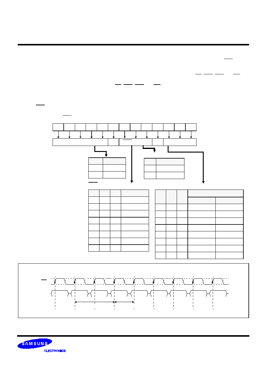
The Bank Activation command is issued by holding CAS and WE high with CS and RAS low at the rising edge of the
clock. The DDR SGRAM has four independent Banks, so two Bank Select addresses(BA
0
, BA
1
) are supported. The Bank
Activation command must be applied before any Read or Write operation is executed. The delay from the Bank Activation
command to the first read or write command must meet or exceed the minimum of RAS to CAS delay time(t
RCD
min
). Once
a bank has been activated, it must be precharged before another Bank Activation command can be applied to the same
bank. The minimum time interval between interleaved Bank Activation commands(Bank A to Bank B and vice versa) is the
Bank to Bank delay time(t
RRD
min
).
BANK ACTIVATION COMMAND
Address
Command
RAS-CAS delay(
t
RCD
)
Bank Activation Command Cycle
(CAS Latency = 2)
Bank A
Row Addr.
Bank A
Col. Addr.
Bank A
Activate
Write A
with Auto
NOP
Precharge
RAS-RAS delay time(
t
RRD
)
Bank A
Row Addr.
Bank B
Row. Addr.
Bank A
Activate
Bank B
Activate
NOP
ROW Cycle Time(
t
RC
)
n
n+1
n+2
2
0
1
: Don
t care
CK, CK
Preliminary
64M DDR SGRAM
K4D623237M
Burst Read operation in DDR SGRAM is in the same manner as the current SDRAM such that the Burst read command
is issued by asserting CS and CAS low while holding RAS and WE high at the rising edge of the clock after t
RCD
from the
bank activation. The address inputs (A
0
~A
7
) determine the starting address for the Burst. The Mode Register sets type of
burst(
S
equential or interleave) and burst length(2, 4, 8, Full page). The first output data is available after the CAS Latency
from the READ command, and the consecutive data are presented on the falling and rising edge of Data Strobe adopted
by DDR SGRAM until the burst length is completed.
BURST READ OPERATION
The Burst Write command is issued by having CS, CAS, and WE low while holding RAS high at the rising edge of the
clock. The address inputs determine the starting column address. There is no real write latency required for burst write
cycle. The first data for burst write cycle must be applied at the first rising edge of the data strobe enabled after t
DQSS
from
the rising edge of the clock that the write command is issued. The remaining data inputs must be supplied on each subse-
quent falling and rising edge of Data Strobe until the burst length is completed. When the burst has been finished, any
additional data supplied to the DQ pins will be ignored.
BURST WRITE OPERATION
Command
< Burst Length=4, CAS Latency=2, 3 >
READ A
NOP
NOP
NOP
NOP
NOP
NOP
NOP
NOP
DQS
DQ
s
CAS Latency=2
Dout 0 Dout 1 Dout 2 Dout 3
DQS
DQ
s
CAS Latency=3
Dout 0 Dout 1 Dout 2 Dout 3
Command
< Burst Length=4 >
NOP
WRITE
NOP
NOP
NOP
NOP
NOP
NOP
NOP
DQS
DQ
s
Din 0
Din 1
Din 2
Din 3
t
DQSS
2
0
1
5
3
4
8
6
7
2
0
1
5
3
4
8
6
7
Ck, Ck
CK, CK
t
DSHZ
t
SDQS
t
ACS
t
SHZ
t
SLZ
Preamble
Postamble
Preamble
Postamble

Preliminary
64M DDR SGRAM
K4D623237M
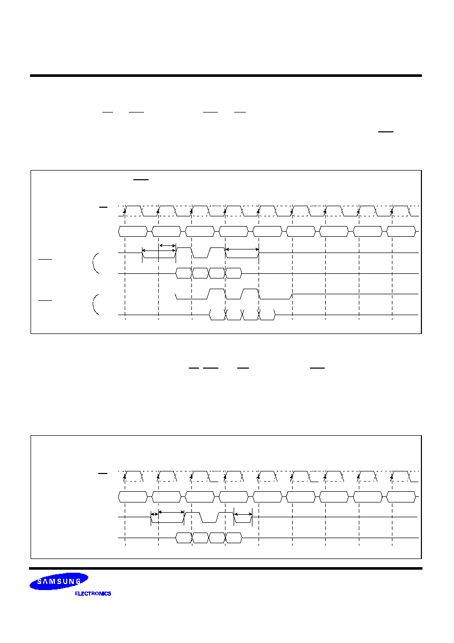
A Burst Read can be interrupted before completion of the burst by new Read command of any bank. When the previous
burst is interrupted, the remaining addresses are overridden by the new address with the full burst length. The data from
the first Read command continues to appear on the outputs until the CAS latency from the interrupting Read command is
satisfied. At this point the data from the interrupting Read command appears. Read to Read interval is minimum 1 tck.
BURST INTERRUPTION
Read Interrupted by a Read
To interrupt a burst read with a write command, Burst stop command must be asserted to avoid data contention on the I/
O bus by placing the DQ
s
(Output drivers) in a high impedance state at least one clock cycle before the Write Command is
initiated.
Read Interrupted by Burst stop & a Write
Command
< Burst Length=4, CAS Latency=2 >
READ A
READ B
NOP
NOP
NOP
NOP
NOP
NOP
NOP
DQS
DQ
s
CAS Latency=2
Dout A
0
Dout A
1
Dout B
0
Dout B
1
Dout B
2
Dout B
3
Command
< Burst Length=4, CAS Latency=2 >
READ
Burst Stop
NOP
WRITE
NOP
NOP
NOP
NOP
DQS
DQ
s
CAS Latency=2
Dout 0
Dout 1
Din 0
Din 1
Din 2
Din 3
CK, CK
CK, CK
2
0
1
5
3
4
8
6
7
2
0
1
5
3
4
8
6
7
NOP
Preliminary
64M DDR SGRAM
K4D623237M
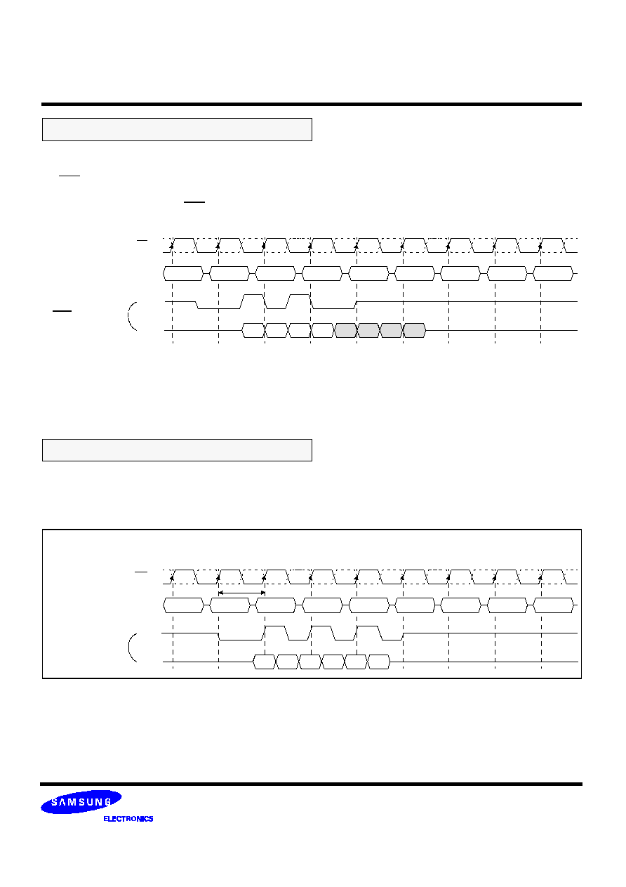
A Burst Read operation can be interrupted by precharge of the same bank. The minimum 1 clock is required for the Read
to precharge intervals without interrupting a Read burst. A precharge command to output disable latency is equivalent to
the CAS latency.
Read Interrupted by a Precharge
Command
< Burst Length=8, CAS Latency=2 >
READ
NOP
Precharge
NOP
NOP
NOP
NOP
NOP
NOP
DQS
DQ
s
CAS Latency=2
Dout 0
Dout 1
Dout 2
Dout 3
A Burst Write can be interrupted before completion of the burst by the new Write Command, with the only restriction being
that the interval that separates the commands must be at least one clock cycle. When the previous burst is interrupted,
the remaining addresses are overridden by the new address and data will be written into the device until the programmed
burst length is satisfied.
Write Interrupted by a Write
Command
< Burst Length=4 >
NOP
WRITE A
WRITE B
NOP
NOP
NOP
NOP
NOP
NOP
DQS
DQ
s
Din A
0
Din A
1
Din B
0
Din B
1
Din B
2
Din B
3
1 tCK interval
Ck, Ck
CK, CK
2
0
1
5
3
4
8
6
7
2
0
1
5
3
4
8
6
7
Dout 4
Dout 5
Dout 6
Dout 7
Interrupted by precharge
Preliminary
64M DDR SGRAM
K4D623237M
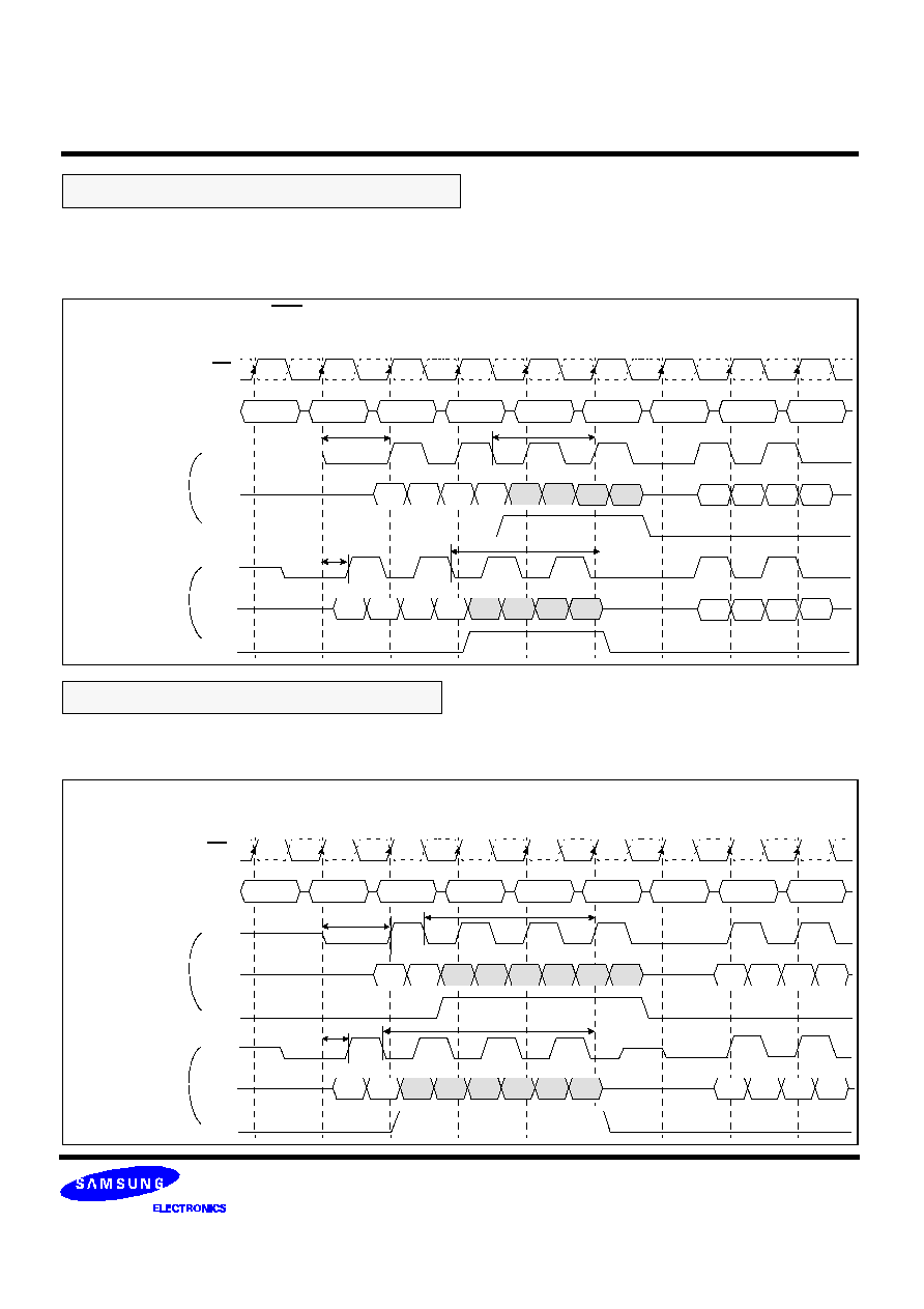
A Burst Write can be interrupted by a Read command to any bank. The DQ
s must be in the high impedance state at
least one clock cycle before interrupting read data appears on the outputs to avoid data contention. When the Read Com-
mand is registered, any residual data from the burst write cycle will be masked by DM. The delay from the last data to Read
command (tCDLR) is required to avoid the data contention DRAM inside.
Write Interrupted by a Read & DM
Command
< Burst Length=8, CAS Latency=2 >
NOP
WRITE
NOP
NOP
READ
NOP
NOP
NOP
NOP
DQS
DQ
s
Din 0
Din 1
Din 2
Din 3
A Burst Write operation can be interrupted before completion of the burst by a precharge of the same bank. A Write
Recovery time(tRDL) is required before a Precharge command to finish the Write operation. When Precharge command is
asserted, any residual data from the burst write cycle must be masked by DM.
Write Interrupted by a Precharge & DM
Din 4
Din 5
Dout 0
Dout 1 Dout 2
Command
< Burst Length=8 >
NOP
WRITE A
NOP
NOP
Precharge
NOP
NOP
NOP
WRITE B
DQS
DQ
s
Dina
0
Dina
1
Dina
2
Dina
3
Dina
4
Dina
5
Dinb
0
Dinb
1
Dinb
2
Dinb
3
Dina
6
Dina
7
Din 6
Din 7
t
CDLRmin
t
RDLmin
t
DQSSmax
DQS
DQ
s
t
CDLRmin
t
DQSSmin
Din 0
Din 1
Din 2
Din 3
Din 4
Din 5
Din 6
Din 7
DM
DQS
DQ
s
t
RDLmax
t
DQSSmin
Dina
0
Dina
1
Dina
2
Dina
3
Dina
4
Dina
5
Dina
6
Dina
7
DM
Dinb
0
Dinb
1
Dinb
2
Dinb
3
t
DQSSmax
Dout 0
Dout 1
Dout 2
CK, CK
CK, CK
Dout 3
Dout 3
2
0
1
5
3
4
8
6
7
2
0
1
5
3
4
8
6
7
Minimum tDQSS
Maximum tDQSS
DM
Minimum tDQSS
Maximum tDQSS
DM

Preliminary
64M DDR SGRAM
K4D623237M
The Burst stop command is initiated by having RAS and CAS high with CS and WE low at the rising edge of the clock
only . The Burst Stop command has the fewest restrictions making it the easiest method to use when terminating a burst
operation before it has been completed. When the Burst Stop command is issued during a burst read cycle, both the data
and DQS(Data Strobe) go to a high impedance state after a delay which is equal to the CAS Latency set in the Mode Reg-
ister. The Burst Stop command, however, is not supported during a write burst operation.
BURST STOP COMMAND
The DDR SGRAM has a Data mask function that can be used in conjunction with data Write cycle only, not Read cycle.
When the Data Mask is activated (DM high) during write operation the write data is masked immediately(DM to Data-mask
Latency is zero).
DM must be issued at the rising edge or the falling edge of Data Strobe instead of a clock edge.
DM FUNCTION
Command
< Burst Length=4, CAS Latency=2, 3 >
READ A
Burst Stop
NOP
NOP
NOP
NOP
NOP
NOP
NOP
DQS
DQ
s
CAS Latency=2
Dout 0 Dout 1
DQS
DQ
s
CAS Latency=3
Command
< Burst Length=8 >
WRITE
NOP
NOP
NOP
NOP
NOP
NOP
NOP
NOP
DQS
DQ
s
Din 0
Din 1
Din 2
Din 3
The burst ends after a delay equal to the CAS latency.
Dout 0 Dout 1
DM
Din 4
Din 5
Din 6
Din7
masked by DM=H
CK, CK
CK, CK
2
0
1
5
3
4
8
6
7
2
0
1
5
3
4
8
6
7
t
DQSSmax

Preliminary
64M DDR SGRAM
K4D623237M
The Auto precharge command can be issued by having column address A
8
High when a Read or a Write command is
asserted into the DDR SGRAM. If A
8
is low when Read or Write command is issued, then normal Read or Write burst oper-
ation is asserted and the bank remains active after the completion of the burst sequence. When the Auto precharge com-
mand is activated, the active bank automatically begins to precharge at the earliest possible moment during read or write
cycle after t
RAS
(min) is satisfied.
AUTO-PRECHARGE OPERATION
Command
< Burst Length=4, CAS Latency=2, 3 >
BANK A
NOP
READ A
NOP
NOP
NOP
NOP
NOP
NOP
DQS
DQ
s
CAS Latency=2
Dout 0 Dout 1 Dout 2 Dout 3
If a Read with Auto-precharge command is initiated, the DDR SGRAM automatically starts the precharge operation on
BL/2 clock later from a Read with Auto-Precharge command when
t
RAS
(min) is satisfied. If not, the start point of precharge
operation will be delayed until
t
RAS
(min) is satisfied. Once the precharge operation has started the bank cannot be reacti-
vated and the new command can not be asserted until the Precharge time(
t
RP
) has been satisfied.
Read with Auto Precharge
ACTIVE
Auto Precharge
* Bank can be reactivated at the
t
RP
completion of
precharge
Begin Auto-Precharge
DQS
DQ
s
CAS Latency=3
Dout 0 Dout 1 Dout 2 Dout 3
When the Read with Auto precharge command is issued, new command can be asserted at T3,T4 and T5 respectively
as follows, even the new command for the same bank is illigal.
Asserted
command
For same Bank
For Different Bank
3
4
5
3
4
5
Read Interrupt
READ +
NO AP*1
READ+
NO AP
Illegal
Legal
Legal
Legal
Active
Illegal
Illegal
Fail
Legal
Legal
Legal
Precharge
Illegal
Illegal
Fail
Legal
Legal
Legal
*1 : AP = Auto Precharge
CK, CK
2
0
1
5
3
4
8
6
7

Preliminary
64M DDR SGRAM
K4D623237M
If A
8
is high when Write command is issued , the write with Auto-Precharge function is performed. Any new command to
the same bank should not be issued until the internal precharge is completed. The internal precharge begins after keeping
t
RDL
(min).
Write with Auto Precharge
Command
< Burst Length=4 >
BANK A
NOP
WRITE A
NOP
NOP
NOP
NOP
NOP
NOP
DQS
DQ
s
Din 0 Din 1 Din 2
ACTIVE
Auto Precharge
* Bank can be reactivated at
completion of
t
RP
t
RDL
t
RP
Internal precharge start
The precharge command is used to precharge or close a bank that has been activated. The precharge command is
issued when CS, RAS and WE are low and CAS is high at the rising edge of the clock, CK. The precharge command can
be used to precharge each bank respectively or all banks simultaneously. The Bank select addresses(BA
0
, BA
1
) are used
to define which bank is precharged when the command is initiated. For write cycle,
t
RDL
(min.) must be satisfied from the
start of the last burst write cycle until the precharge command can be issued. After
t
RP
from the precharge, an active com-
mand to the same bank can be initiated.
PRECHARGE COMMAND
< Bank Selection for Precharge by Bank address bits >
A
8
/AP
BA1
BA
0
Precharge
0
0
0
Bank A Only
0
0
1
Bank B Only
0
1
0
Bank C Only
0
1
1
Bank D Only
1
X
X
All Banks
CK, CK
< Block Write >
CK, CK
CMD
t
BPL
t
RP
Auto Precharge Starts
BW
2
0
1
5
3
4
8
6
7
2
0
1
5
3
4
8
6
7
Din 3
Preliminary
64M DDR SGRAM
K4D623237M
Command
CKE
PRE
t
RP
t
RC
A Self Refresh command is defined by having CS, RAS, CAS and CKE held low with WE high at the rising edge of the
clock. Once the self Refresh command is initiated, CKE must be held low to keep the device in Self Refresh mode. After 1
clock cycle from the self refresh command, all of the external control signals including system clock(CK, CK) can be dis-
abled except CKE. The clock is internally disabled during Self Refresh operation to reduce power. To exit the Self Refresh
mode, supply stable clock input before returning CKE high, assert deselect or NOP command and then assert CKE high.
The Auto Refresh is required before self refresh entry and after self refresh exit.
SELF REFRESH
Auto
=High
Refresh
CMD
Command
CKE
Stable Clock
t
IS
Auto
Refresh
NOP
Self
Refresh
An Auto Refresh command is issued by having CS, RAS and CAS held low with CKE and WE high at the rising edge of
the clock, CK. All banks must be precharged and idle for a
t
RP
(min) before the Auto Refresh command is applied. No con-
trol of the external address pins is required once this cycle has started because of the internal address counter. When the
refresh cycle has completed, all banks will be in the idle state. A delay between the Auto Refresh command and the next
Activate Command or subsequent Auto Refresh Command must be greater than or equal to the
t
RFC(
min).
AUTO REFRESH
CK, CK
CK, CK
t
RC(min)
t
IS
2
0
1
5
3
4
8
6
7
11
9
10

Preliminary
64M DDR SGRAM
K4D623237M
CKE
Precharge
Active
The power down is entered when CKE Low,and exited when CKE High. Once the power down mode is initiated, all of the
receiver circuits except CK and CKE are gated off to reduce power consumption. The both bank should be in idle state
prior to entering the precharge power down mode and CKE should be set high at least 1 tCK+tIS prior to Row active com-
mand. During power down mode, refresh operations cannot be performed, therefore the device cannot remain in power
down mode longer than the refresh period(t
REF
) of the device.
POWER DOWN MODE
power
Entry
down
Precharge
Command
CK, CK
t
IS
t
IS
t
IS
t
IS
2
0
1
5
3
4
8
6
7
12
10
11
13
14
9
power
Exit
down
Precharge
power
Entry
down
Active
power
Exit
down
Active
Read
(NOP)
Preliminary
64M DDR SGRAM
K4D623237M
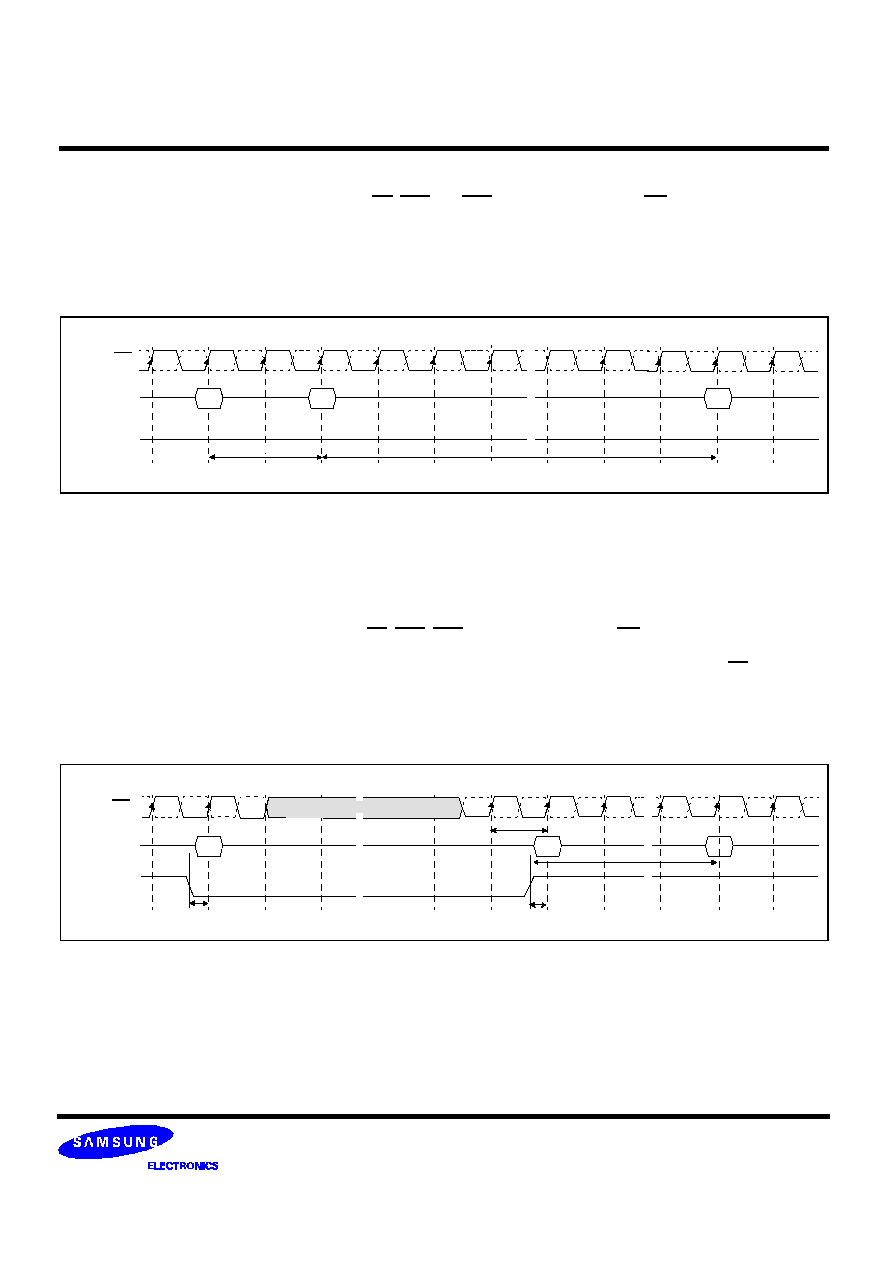
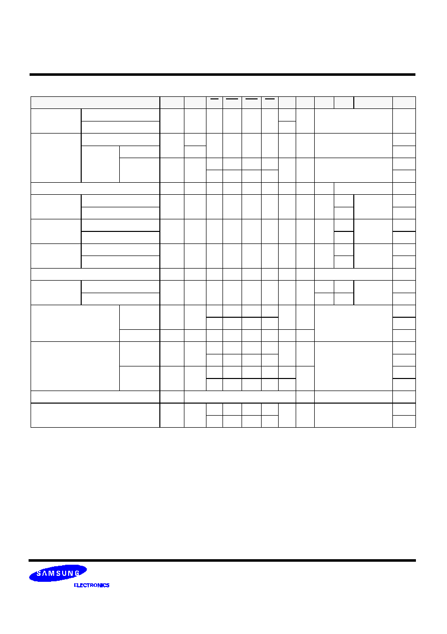
SIMPLIFIED TRUTH TABLE
(V=Valid, X=Don
t Care, H=Logic High, L=Logic Low)
COMMAND
CKEn-1 CKEn
CS
RAS
CAS
WE
DSF
DM
BA
0,1
A
8
/AP A
10
,A
9
,A
7
~A
0
Note
Register
Mode Register Set
H
X
L
L
L
L
L
X
OP CODE
1, 2
Special Mode Register Set
H
Refresh
Auto Refresh
H
H
L
L
L
H
X
X
X
3
Self
Refresh
Entry
L
3
Exit
L
H
L
H
H
H
X
X
X
3
H
X
X
X
3
Bank Active & Row Addr.
H
X
L
L
H
H
X
X
V
Row Address
Read &
Column Address
Auto Precharge Disable
H
X
L
H
L
H
X
X
V
L
Column
Address
4
Auto Precharge Enable
H
4
Write &
Column Address
Auto Precharge Disable
H
X
L
H
L
L
L
X
V
L
Column
Address
4
Auto Precharge Enable
H
4, 6
Block Write &
Column Address
Auto Precharge Disable
H
X
L
H
L
L
H
X
V
L
Column
Address
4, 5
Auto Precharge Enable
H
4,5,6,9
Burst Stop
H
X
L
H
H
L
X
X
X
7
Precharge
Bank Selection
H
X
L
L
H
L
X
X
V
L
X
All Banks
X
H
5
Active Power Down
Entry
H
L
H
X
X
X
X
X
X
L
V
V
V
Exit
L
H
X
X
X
X
X
X
Precharge Power Down Mode
Entry
H
L
H
X
X
X
X
X
X
L
H
H
H
Exit
L
H
H
X
X
X
X
X
L
H
H
H
X
DM
H
X
V
X
8
No Operation Command
H
X
H
X
X
X
X
X
X
L
H
H
H
1. OP Code : Operand Code
A
0
~ A
10
& BA
0
~ BA
1
: Program keys. (@MRS)
A
6
: LCR @ SMRS/Color register exists only one per DQi which all banks share.
Color is loaded into chip through DQ pin
2. MRS can be issued only at all banks precharge state.
SMRS can be issued only if DQ
s are idle.
A new command can be issued after 1 clock cycle of MRS/SMRS.
3. Auto refresh functions are as same as CBR refresh of DRAM.
The automatical precharge without row precharge command is meant by "Auto".
Auto/self refresh can be issued only at all banks precharge state.
Note :

Preliminary
64M DDR SGRAM
K4D623237M
4. BA
0
~ BA
1
: Bank select addresses.
If both BA
0
and BA
1
are "Low" at read, write, row active and precharge, bank A is selected.
If BA
0
is "High" and BA
1
is "Low" at read, write, row active and precharge, bank B is selected.
If BA
0
is "Low" and BA
1
is "High" at read, write, row active and precharge, bank C is selected.
If both BA
0
and BA
1
are "High" at read, write, row active and precharge, bank D is selected.
5. If A
8
/AP is "High" at row precharge, BA
0
and BA
1
is ignored and all banks are selected.
6. During burst write with auto precharge, new read/write command can not be issued.
Another bank read/write command can be issued after the end of burst.
New row active of the associated bank can be issued at t
RP
after the end of burst.
7. Burst stop command is valid at every burst length.
8. DM sampled at the rising and falling edges of the DQS and Data-in are masked at the both edges (Write DM latency is 0).
9. Graphic features are added to SDRAM
s original features.
If DSF is tied to low, graphic functions are disabled and chip operates as a 64M SDRAM with 32 DQ
s.

Preliminary
64M DDR SGRAM
K4D623237M
FUNCTION TRUTH TABLE
Current State CS RAS CAS WE DSF
Address
Command
Action
IDLE
H
X
X
X
X
X
DESEL
NOP
L
H
H
H
X
X
NOP
NOP
L
H
H
L
X
X
TERM
NOP
L
H
L
X
X
BA, CA, A
8
READ/WRITE/BW
ILLEGAL*2
L
L
H
H
X
BA, RA
ACT
Bank Active, Latch RA
L
L
H
L
X
BA, A
8
PRE/PREA
NOP*4
L
L
L
H
X
X
REFA
AUTO-Refresh*5
L
L
L
L
L
Op-Code, Mode-Add
MRS
Mode Register Set*5
H
SMRS
Special Mode Register Set
ROW ACTIVE H
X
X
X
X
X
DESEL
NOP
L
H
H
H
X
X
NOP
NOP
L
H
H
L
X
X
TERM
NOP
L
H
L
H
X
BA, CA, A
8
READ/READA
Begin Read, Latch CA,
Determine Auto-Precharge
L
H
L
L
L
BA, CA, A
8
WRITE/WRITEA
Begin Write, Latch CA,
Determine Auto-Precharge
L
H
L
L
H
BA, CA, A
8
BW/BWA
Begin Block Write, Latch CA,
Determine Auto-Precharge
L
L
H
H
X
BA, RA
ACT
ILLEGAL*2
L
L
H
L
X
BA, A
8
PRE/PREA
Precharge/Precharge All
L
L
L
H
X
X
REFA
ILLEGAL
L
L
L
L
L
Op-Code, Mode-Add
MRS
ILLEGAL
H
SMRS
Special Mode Register Set
READ
H
X
X
X
X
X
DESEL
NOP(Continue Burst to END)
L
H
H
H
X
X
NOP
NOP(Continue Burst to END)
L
H
H
L
X
X
TERM
Terminate Burst
L
H
L
H
L
BA, CA, A
8
READ/READA
Terminate Burst, Latch CA,
Begin New Read, Determine
Auto-Precharge*3
L
H
L
L
X
BA, CA, A
8
WRITE/WRITEA
BW/BWA
ILLEGAL
L
L
H
H
L
BA, RA
ACT
ILLEGAL*2
L
L
H
L
L
BA, A
8
PRE/PREA
Terminate Burst, Precharge
L
L
L
H
X
X
REFA
ILLEGAL
L
L
L
L
L
Op-Code, Mode-Add
MRS
ILLEGAL
H
SMRS
ILLEGAL

Preliminary
64M DDR SGRAM
K4D623237M
FUNCTION TRUTH TABLE
(continued)
Current State
CS RAS CAS WE DSF
Address
Command
Action
WRITE
H
X
X
X
X
X
DESEL
NOP(Continue Burst END)
L
H
H
H
X
X
NOP
NOP(Continue Burst END)
L
H
H
L
X
X
TERM
ILLEGAL
L
H
L
H
X
BA, CA, A
8
READ/READA
Terminate Burst With DM=High,
Latch CA, Begin Read, Determine
Auto-Precharge*3
L
H
L
L
L
BA, CA, A
8
WRITE/WRITEA
Terminate Burst, Latch CA,
Begin new Write, Determine Auto-
Precharge*3
L
H
L
L
H
BA, CA, A
8
BW/BWA
Terminate Burst , Latch CA,
New Block Write, Determine AP.
L
L
H
H
X
BA, RA
ACT
ILLEGAL*2
L
L
H
L
X
BA, A
8
PRE/PREA
Terminate Burst With DM=High,
Precharge
L
L
L
H
X
X
REFA
ILLEGAL
L
L
L
L
L
Op-Code, Mode-Add
MRS
ILLEGAL
H
SMRS
ILLEGAL
READ with AUTO
PRECHARGE
H
X
X
X
X
X
DESEL
NOP(Continue Burst END)
L
H
H
H
X
X
NOP
NOP(Continue Burst END)
L
H
H
L
X
X
TERM
ILLEGAL
L
H
L
X
X
BA, CA, A
8
READ/WRITE
ILLEGAL*2
L
L
H
H
X
BA, RA
ACT
ILLEGAL*2
L
L
H
L
X
BA, A
8
PRE/PREA
ILLEGAL*2
L
L
L
H
X
X
REFA
ILLEGAL
L
L
L
L
L
Op-Code, Mode-Add
MRS
ILLEGAL
H
SMRS
ILLEGAL
WRITE with AUTO
RECHARGE
H
X
X
X
X
X
DESEL
NOP(Continue Burst to END)
L
H
H
H
X
X
NOP
NOP(Continue Burst to END)
L
H
H
L
X
X
TERM
ILLEGAL
L
H
L
X
X
BA, CA, A
8
READ/WRITE
ILLEGAL*2
L
L
H
H
X
BA, RA
ACT
ILLEGAL*2
L
L
H
L
X
BA, A
8
PRE/PREA
ILLEGAL*2
L
L
L
H
X
X
REFA
ILLEGAL
L
L
L
L
L
Op-Code, Mode-Add
MRS
ILLEGAL
H
SMRS
ILLEGAL

Preliminary
64M DDR SGRAM
K4D623237M
FUNCTION TRUTH TABLE
(continued)
Current State
CS
RAS CAS
WE
DSF
Address
Command
Action
BLOCK
WRITE
RECOVERING
H
X
X
X
X
X
DESEL
NOP(Continue Block Write)
L
H
H
H
X
X
NOP
NOP(Continue Block Write)
L
H
H
L
X
X
TERM
NOP
L
H
L
X
X
BA, CA, A
8
READ/READA
WRITE/
WRITEA
ILLEGAL
L
L
H
H
X
BA, RA
ACT
ILLEGAL*2
L
L
H
L
X
BA, A
8
PRE/PREA
Terminate Block Write, Pre-
charge
L
L
L
H
X
X
REFA
ILLEGAL
L
L
L
L
L
Op-Code, Mode-Add
MRS
ILLEGAL
H
SMRS
ILLEGAL
PRE-
CHARGING
H
X
X
X
X
X
DESEL
NOP(Idle after
t
RP
)
L
H
H
H
X
X
NOP
NOP(Idle after
t
RP
)
L
H
H
L
X
X
TERM
NOP
L
H
L
X
X
BA, CA, A
8
READ/WRITE
ILLEGAL*2
L
L
H
H
X
BA, RA
ACT
ILLEGAL*2
L
L
H
L
X
BA, A
8
PRE/PREA
NOP*4(Idle after
t
RP
)
L
L
L
H
X
X
REFA
ILLEGAL
L
L
L
L
L
Op-Code, Mode-Add
MRS
ILLEGAL
H
SMRS
ILLEGAL
ROW
ACTIVATING
H
X
X
X
X
X
DESEL
NOP(ROW Active after
t
RCD
)
L
H
H
H
X
X
NOP
NOP(ROW Active after
t
RCD
)
L
H
H
L
X
X
TERM
NOP
L
H
L
X
X
BA, CA, A
8
READ/WRITE
ILLEGAL*2
L
L
H
H
X
BA, RA
ACT
ILLEGAL*2
L
L
H
L
X
BA, A
8
PRE/PREA
ILLEGAL*2
L
L
L
H
X
X
REFA
ILLEGAL
L
L
L
L
L
Op-Code, Mode-Add
MRS
ILLEGAL
H
SMRS
ILLEGAL

Preliminary
64M DDR SGRAM
K4D623237M
FUNCTION TRUTH TABLE
(continued)
ABBREVIATIONS :
H=High Level, L=Low level, V=Valid, X=Don
t Care
BA=Bank Address, RA=Row Address, CA=Column Address, NOP=No Operation
Note :
1. All entries assume that CKE was High during the preceding clock cycle and the current clock cycle.
2. ILLEGAL to bank in specified state ; function may be legal in the bank indicated by BA, depending on the state of that bank.
3. Must satisfy bus contention, bus turn around, write recovery requirements.
4. NOP to bank precharging or in idle sate. May precharge bank indicated by BA.
5. ILLEGAL if any bank is not idle.
6. Same Bank
s previous Auto precharge will not be performed. But if Bank is different, previous Auto precharge will be performed.
ILLEGAL = Device operation and/or data-integrity are not guaranteed.
Current State
CS RAS
CAS WE DSF
Address
Command
Action
WRITE
RECOVERING
H
X
X
X
X
X
DESEL
NOP
L
H
H
H
X
X
NOP
NOP
L
H
H
L
X
X
TERM
NOP
L
H
L
H
X
BA, CA, A
8
READ
ILLEGAL*2
L
H
L
L
L
BA, CA, A
8
WRITE/WRITEA
New Write, Determine AP.
L
H
L
L
H
BA, CA, A
8
BW/BWA
New BW, Determine AP.
L
L
H
H
X
BA, RA
ACT
ILLEGAL*2
L
L
H
L
X
BA, A
8
PRE/PREA
ILLEGAL*2
L
L
L
H
X
X
REFA
ILLEGAL
L
L
L
L
L
Op-Code, Mode-Add
MRS
ILLEGAL
H
SMRS
ILLEGAL
RE-
FRESHING
H
X
X
X
X
X
DESEL
NOP(Idle after
t
RP
)
L
H
H
H
X
X
NOP
NOP(Idle after
t
RP
)
L
H
H
L
X
X
TERM
NOP
L
H
L
X
X
BA, CA, A
8
READ/WRITE
ILLEGAL
L
L
H
H
X
BA, RA
ACT
ILLEGAL
L
L
H
L
X
BA, A
8
PRE/PREA
ILLEGAL
L
L
L
H
X
X
REFA
ILLEGAL
L
L
L
L
L
Op-Code, Mode-Add
MRS
ILLEGAL
H
SMRS
ILLEGAL
Preliminary
64M DDR SGRAM
K4D623237M
FUNCTION TRUTH TABLE for CKE
ABBREVIATIONS :
H=High Level, L=Low level, X=Don
t Care
Note :
1. After CKE
s low to high transition to exist self refresh mode. And a time of tRC(min) has to be elapse after CKE
s low to high
transition to issue a new command.
2. CKE low to high transition is asynchronous as if restarts internal clock.
A minimum setup time "tSS + one clock" must be satisfied before any command other than exit.
3. Power-down and self refresh can be entered only from the all banks idle state.
4. Must be a legal command.
Current State
CKE
n-1
CKE
n
CS
RAS
CAS
WE
DSF
Add
Action
SELF-
REFRESHING
H
X
X
X
X
X
X
X
INVALID
L
H
H
X
X
X
X
X
Exit Self-Refresh*1
L
H
L
H
H
H
X
X
Exit Self-Refresh*1
L
H
L
H
H
L
X
X
ILLEGAL
L
H
L
H
L
X
X
X
ILLEGAL
L
H
L
L
X
X
X
X
ILLEGAL
L
L
X
X
X
X
X
X
NOP(Maintain Self-Refresh)
Both Bank
Precharge
POWER
DOWN
H
X
X
X
X
X
X
X
INVALID
L
H
H
X
X
X
X
X
Exit Power Down*2
L
H
L
H
H
H
X
X
Exit Power Down*2
L
H
L
H
H
L
X
X
ILLEGAL
L
H
L
H
L
X
X
X
ILLEGAL
L
H
L
L
X
X
X
X
ILLEGAL
L
L
X
X
X
X
X
X
NOP(Maintain Power Down)
ALL BANKS
IDLE
H
H
X
X
X
X
X
X
Refer to Function True Table
H
L
H
X
X
X
X
X
Enter Power Down*3
H
L
L
H
H
H
X
X
Enter Power Down*3
H
L
L
H
H
L
X
X
ILLEGAL
H
L
L
H
L
X
X
X
ILLEGAL
H
L
L
L
H
H
L
RA
Row (& Bank) Active
H
L
L
L
L
H
L
X
Enter Self-Refresh*3
H
L
L
L
L
L
L
OP Code
Mode Register Access
H
L
L
L
L
L
H
OP Code
Special Mode Register Access
L
X
X
X
X
X
X
X
Refer to Current State=Power Down
Any State
other than
listed above
H
H
X
X
X
X
X
X
Refer to Function True Table
H
L
X
X
X
X
X
X
Begin Clock Suspend next cycle*4
L
H
X
X
X
X
X
X
Exit Clock Suspend next cycle*4
L
L
X
X
X
X
X
X
Maintain Clock Suspend

Preliminary
64M DDR SGRAM
K4D623237M
READ
SIMPLIFIED STATE DIAGRAM
SELF
REFRESH
AUTO
REFRESH
POWER
DOWN
ROW
ACTIVE
READA
WRITEA
WRITEA
PRE
CHARGE
POWER
ON
IDLE
MODE
POWER
DOWN
REGISTER
SET
REFS
REFSX
REFA
MRS
CKEL
CKEH
ACT
CKEL
CKEH
WRITE
WRITE
WRITEA
PRE
PRE
POWER
APPLIED
READA
PRE
PRE
READA
READA
READ
READ
Automatic Sequence
Command Sequence
/BW
/BWA
/BW
/BWA
WRITEA
/BWA
BST

Preliminary
64M DDR SGRAM
K4D623237M
ABSOLUTE MAXIMUM RATINGS
Parameter
Symbol
Value
Unit
Voltage on any pin relative to Vss
V
IN
, V
OUT
-1.0 ~ 4.6
V
Voltage on V
DD
supply relative to Vss
V
DD
, V
DDQ
-1.0 ~ 4.6
V
Storage temperature
T
STG
-55 ~ +150
∞
C
Power dissipation
P
D
1.6
W
Short circuit current
I
OS
50
mA
Permanent device damage may occur if ABSOLUTE MAXIMUM RATINGS are exceeded.
Functional operation should be restricted to recommended operating condition.
Exposure to higher than recommended voltage for extended periods of time could affect device reliability.
Note :
POWER & DC OPERATING CONDITIONS(SSTL_2 In/Out)
Recommended operating conditions(Voltage referenced to V
SS
=0V, T
A
=0 to 65
∞
C)
Parameter
Symbol
Min
Typ
Max
Unit
Note
Device Supply voltage
V
DD
3.135
3.3
3.465
V
1
Output Supply voltage
V
DDQ
2.375
2.50
2.625
V
1
Reference voltage
V
REF
1.15
1.25
1.35
V
2, 3
Termination voltage
Vtt
V
REF
-0.04
V
REF
V
REF
+0.04
V
4
Input logic high voltage
V
IH
V
REF
+0.18
-
V
DDQ
+0.30
V
Input logic low voltage
V
IL
-0.30
-
V
REF
-0.18
V
5
Output logic high voltage
V
OH
Vtt+0.76
-
-
V
I
OH
=-15.2mA
Output logic low voltage
V
OL
-
-
Vtt-0.76
V
I
OL
=+15.2mA
Input leakage current
I
IL
-5
-
5
uA
6
Output leakage current
I
OL
-5
-
5
uA
6
1. Under all conditions V
DDQ
must be less than or equal to V
DD
.
2. Typically, the value of V
REF
is expected to be about 0.50*V
DDQ
of the transmitting device.
V
REF
is expected to track variation in V
DDQ
.
3. Peak to peak AC noise on V
REF
may not exceed 2% V
REF
(DC).
4. V
tt
of the transmitting device must track V
REF
of the receiving device.
5. V
IL
(min.)= -1.5V AC(pulse width
5ns).
6. For any pin under test input of 0V
V
IN
V
DD
+0.3V is acceptable.
For all other pins that are not under test V
IN
=0V.
Note :

Preliminary
64M DDR SGRAM
K4D623237M
AC CHARACTERISTICS
Simplified Timing(1) @ BL=4, CL=2
Parameter
Symbol
-60
-70
-80
-10
Unit
Note
Min
Max
Min
Max
Min
Max
Min
Max
CK cycle time
CL=2
t
CK
12
1000
12
1000
12
1000
13
1000
ns
CL=3
6
7
8
10
ns
CK high level width
t
CH
0.4
0.6
0.4
0.6
0.4
0.6
0.4
0.6
tCK
CK low level width
t
CL
0.4
0.6
0.4
0.6
0.4
0.6
0.4
0.6
tCK
CK rising edge to CK rising edge Delay
t
CCB
0.45
0.55
0.45
0.55
0.45
0.55
0.45
0.55
tCK
CK Edge to Data Strobe Edge
t
ACS
2.5
5.5
2.5
5.5
2.5
6.0
2.5
6.0
ns
CK Edge to Output Data Edge
t
AC
2.5
5.5
2.5
5.5
2.5
6.0
2.5
6.0
ns
Data Strobe Edge to Ouput Data Edge
t
DQSQ
-0.4
+0.4
-0.5
+0.5
-0.5
+0.5
-0.6
+0.6
ns
Data valid widow
t
DVQ
1.9
2.1
2.6
3.3
ns
Data strobe valid window
t
DVQS
1.9
2.1
2.6
3.3
ns
DQS Low-Z to 1st valid DQS(Preamble) @ Read
t
SLZ
4
8
5
9
6
10
8
12
ns
Last valid DQS to DQS Hi-Z(Postamble) @ Read
t
SHZ
4
8
5
9
6
10
8
12
ns
Last valid DQS to DQS Hi-Z(Postamble) @ Write
t
DSHZ
2
2.5
3
4
ns
Data out active to Hi-Z
t
HZQ
3
3
3
3
ns
DQS Write Preamble setup time
t
SDQS
0
0
0
0
ns
CK to valid DQS-in
t
DQSS
3.5
1 tCK
4
1 tCK
4
1 tCK
4.5
1 tCK
ns
DQS-in high level width
t
SIH
0.4
0.6
0.4
0.6
0.4
0.6
0.4
0.6
tCK
DQS-in low level width
t
SIL
0.4
0.6
0.4
0.6
0.4
0.6
0.4
0.6
tCK
DQS-in cycle time
t
SIC
1
1
1
1
tCK
Input setup time
t
IS
1.5
1.75
2
2.5
ns
Input hold time
t
IH
1
1
1
1
ns
Data in & DM set-up time
t
DS
0.4
0.4
0.4
0.6
ns
Data in & DM hold time
t
DH
0.7
0.7
0.8
1
ns
CK transition time
t
T
0.5
1.5
0.5
1.7
0.5
2
0.5
2.5
ns
1
3
4
6
7
tCCB
tCL
tCK
tACS
Hi-Z
Hi-Z
CK, CK
DQS
DQ
CS
DM
2
5
tIS
tIH
tAC
8
tDS tDH
0
1
Qa0
tDQSQ
tSHZ
tSLZ
Db0
Db1
Db2
Db3
tDVQS
tSIC
tDQSS
tSIH
tSIL
tDS tDH
tHZQ
tCH
tDVQ
Qa1
Qa2
Qa3
tSDQS
tDSHZ
COMMAND
READ
WRITE

Preliminary
64M DDR SGRAM
K4D623237M
AC CHARACTERISTICS
1. Note : When t
DQSS
is close to the minimum value, t
CDLR
and t
RDL
are 2 tck ,3 tck, respectively.
When t
DQSS
is close to the maximum value, t
CDLR
and t
RDL
are 1.5 tck, 2.5 tck respectively.
For normal write operation, even numbers of Din are to be written inside DRAM.
Simplified Timing(2) @ BL=4, CL=2
Parameter
Symbol
-60
-70
-80
-10
Unit
Note
Min
Max
Min
Max
Min
Max
Min
Max
Row cycle time
t
RC
70
70
70
70
ns
Row active time
t
RAS
48
100K
49
100K
48
100K
50
100K
ns
RAS to CAS delay
t
RCD
18
20
20
20
ns
Row precharge time
t
RP
18
21
20
20
ns
Row active to Row active delay
t
RRD
12
14
16
20
ns
Last data in to Row precharge
t
RDL
3.5 tCK
-
t
DQSS
3.5 tCK
-
t
DQSS
3.5 tCK
-
t
DQSS
3.5 tCK
-
t
DQSS
ns
1
Last data in to Read command delay
t
CDLR
2.5 tCK
-
t
DQSS
2.5 tCK
-
t
DQSS
2.5 tCK
-
t
DQSS
2.5 tCK
-
t
DQSS
ns
1
Last data in to Write command delay
t
CDLW
0
0
0
0
tCK
Col. address to Col. address delay
t
CCD
1
1
1
1
tCK
Mode register set cycle time
t
MRD
1
1
1
1
tCK
Special Mode register set cycle time
t
SMRD
1
1
1
1
tCK
Block write cycle
t
BWC
1
1
1
1
tCK
Block write to precharge
t
BPL
4
4
4
4
tCK
Qa0 Qa1 Qa2 Qa3
0
1
2
3
4
5
6
7
8
BAa
Ra
Ra
tRCD
ACTIVE
ACTIVE
WRITE
WRITE
Qa0 Qa1 Qa2 Qa3
Qb0 Qb1
Qb3
13
14
15
16
17
18
19
20
21
BAa
BAb
Ca
Cb
tCCD
BAa
Ca
9
10
11
12
PRECH
BAa
22
READ
BAa
Ra
Ra
Qa0 Qa1 Qa2 Qa3
Normal Write Burst
(@ BL=4)
Multi Bank Interleaving Write Burst
(@ BL=4)
Write Interrupted by Read
(@ CL=2, BL=4)
BAa
Ra
Ra
BAb
Rb
Rb
Qb2
tCDLR
tRAS
tRC
tRP
tRRD
COMMAND
DQS
DQ
WE
DM
CK, CK
A8/AP
ADDR
(A0~A7,
BA[1:0]
A9,A10)
ACTIVE
WRITE

Preliminary
64M DDR SGRAM
K4D623237M
DC CHARACTERISTICS
Note : 1. Measured with outputs open.
2. Refresh period is 16ms.
3. Assumes minimum column address update cycle
t
BWC
(min).
Parameter
Symbol
Test Condition
CAS
Latency
Version
Unit
Note
-60
-70
-80
-10
Operating Current
(One Bank Active)
I
CC1
Burst Lenth=2
t
RC
t
RC
(min)
I
OL
=0mA
260
240
220
200
mA
1
Precharge Standby Current in
Power-down mode
I
CC2
P
CKE
V
IL
(max),
t
CC
=10ns
2
mA
I
CC2
PS
CKE
V
IL
(max), CK
V
IL
(min),
t
CC
=
2
Precharge Standby Current
in Non Power-down mode
I
CC2
N
CKE
V
IH
(min), CS
V
IH
(min),
t
CC
=10ns Input signals are changed
once
65
mA
I
CC2
NS
CKE
V
IH
(min),CK
V
IL
(max),
t
CC
=
20
Active Standby Current
power-down mode
I
CC3
P
CKE
V
IL
(max),
t
CC
=10ns
4
mA
I
CC3
PS
CKE
VIL(max),CK
VIL(max),
t
CC
=
4
Active Standby Current in
in Non Power-down mode
I
CC3
N
CKE
VIH(min), CS
VIH(min),
t
CC
=10ns Input signals are changed
once
65
mA
I
CC3
NS
CKE
VIH(min),CK
VIL(max),
t
CC
=
Input signals are stable.
40
Operating Current
(Burst Mode)
I
CC4
I
OL
=0mA
Page Burst
All Banks activated
t
CCD
=2 tck
3
400
360
320
280
mA
1
2
300
300
300
280
Refresh Current
I
CC5
t
RC
t
RC
(min)
300
290
280
270
mA
2
Self Refresh Current
I
CC6
CKE
0.2V
2
mA
Operating Current
(One Bank Block Write)
I
CC7
t
CC
t
CC
(min)
,
I
OL
=0mA
,
t
BWC
(min)
420
380
340
300
mA
3
Recommended operating conditions Unless Otherwise Noted, T
A
=0 to 65
∞
C)

Preliminary
64M DDR SGRAM
K4D623237M
AC OPERATING TEST CONDITIONS
(V
DD
=3.3V
±
0.15V, T
A
= 0 to 65
∞
C)
Parameter
Value
Unit
Note
Input reference voltage for CK(for single ended)
0.50*V
DDQ
V
CK signal maximum peak swing
1.5
V
CK signal minimum slew rate
1.0
V/ns
Input Levels(V
IH
/V
IL
)
V
REF
+0.35/V
REF
-0.35
V
Input timing measurement reference level
V
REF
V
Output timing measurement reference level
V
tt
V
Output load condition
See Fig.1
CAPACITANCE
(V
DD
=3.3V, T
A
= 25
∞
C,
f=1MHz)
Parameter
Symbol
Min
Max
Unit
Input capacitance(A
0
~A
10
, BA
0
~BA
1
)
C
IN1
2.5
4.5
pF
Input capacitance
(
CK, CKE, CS, RAS,CAS, WE )
C
IN2
2.5
5.0
pF
Data & DQS input/output capacitance(DQ
0
~DQ
31
)
C
OUT
2.5
5.5
pF
Input capacitance(DM)
C
IN3
2.5
5.5
pF
R
T
=50
Output
C
LOAD
=30pF
(Fig. 1) Output Load Circuit
Z0=50
V
REF
=0.5*V
DDQ
V
tt
=0.5*V
DDQ
DECOUPLING CAPACITANCE GUIDE LINE
Recommended decoupling capacitance added to power line at board.
Parameter
Symbol
Value
Unit
Decoupling Capacitance between V
DD
and V
SS
C
DC1
0.1 + 0.01
uF
Decoupling Capacitance between V
DDQ
and V
SSQ
C
DC2
0.1 + 0.01
uF
1. V
DD
and V
DDQ
pins are separated each other.
All V
DD
pins are connected in chip. All V
DDQ
pins are connected in chip.
2. V
SS
and V
SSQ
pins are separated each other
All V
SS
pins are connected in chip. All V
SSQ
pins are connected in chip.
Note :

Preliminary
64M DDR SGRAM
K4D623237M
Basic Timing (Setup, Hold and Access Time @BL=4, CL=2)
1
3
4
6
7
t
C
C
B
t
C
L
t
C
K
t
C
H
t
C
L
t
C
K
t
A
C
S
H
i
-
Z
H
i
-
Z
C
K
,
C
K
C
O
M
M
A
N
D
D
Q
S
D
Q
C
K
E
C
S
B
A
[
1
:
0
]
A
8
/
A
P
A
D
D
R
W
E
D
M
R
A
S
C
A
S
2
5
(
A
0
~
A
7
,
A
9
,
A
1
0
)
B
A
a
B
A
b
C
a
C
b
t
I
S
t
I
H
R
E
A
D
W
R
I
T
E
t
A
C
8
H
I
G
H
t
D
S
t
D
H
0
1
Q
a
0
t
D
Q
S
Q
t
S
H
Z
t
S
L
Z
D
b
0
D
b
1
D
b
2
D
b
3
t
D
V
Q
S
t
S
I
C
t
D
Q
S
S
t
S
I
H
t
S
I
L
t
D
S
t
D
H
t
H
Z
Q
t
C
H
t
D
V
Q
Q
a
1
Q
a
2
Q
a
3
t
S
D
Q
S
t
D
S
H
Z

Preliminary
64M DDR SGRAM
K4D623237M
Multi Bank Interleaving READ (@BL=4, CL=2)
A
C
T
I
V
E
A
C
T
I
V
E
R
E
A
D
R
E
A
D
Q
a
0
Q
a
1
Q
a
2
Q
a
3
Q
b
0
Q
b
1
Q
b
2
Q
b
3
C
O
M
M
A
N
D
D
Q
S
D
Q
0
1
2
3
4
5
6
7
8
C
K
E
C
S
W
E
D
M
R
A
S
C
A
S
B
A
a
B
A
b
B
A
a
B
A
b
R
a
R
b
R
a
R
b
C
a
C
b
t
R
R
D
t
R
C
D
H
I
G
H
t
R
C
D
t
C
C
D
t
C
A
C
C
K
,
C
K
A
8
/
A
P
A
D
D
R
(
A
0
~
A
7
,
A
9
,
A
1
0
)
B
A
[
1
:
0
]

Preliminary
64M DDR SGRAM
K4D623237M
Multi Bank Interleaving WRITE (@BL=4)
C
O
M
M
A
N
D
D
Q
S
D
Q
C
K
E
C
S
W
E
D
M
R
A
S
C
A
S
A
C
T
I
V
E
R
a
A
C
T
I
V
E
R
b
W
R
I
T
E
C
a
B
A
a
B
A
b
B
A
a
B
A
b
R
a
H
I
G
H
R
b
C
b
D
a
0
D
a
1
D
a
2
D
a
3
D
b
0
D
b
1
D
b
2
D
b
3
t
R
R
D
t
R
C
D
t
R
C
D
t
C
C
D
C
K
,
C
K
A
8
/
A
P
A
D
D
R
(
A
0
~
A
7
,
A
9
,
A
1
0
)
B
A
[
1
:
0
]
W
R
I
T
E
0
1
2
3
4
5
6
7
8
Preliminary
64M DDR SGRAM
K4D623237M
Auto Precharge after READ Burst (@BL=8)
C
O
M
M
A
N
D
C
K
E
C
S
W
E
D
M
R
A
S
C
A
S
t
R
P
R
E
A
D
A
C
T
I
V
E
Q
a
0
Q
a
1
Q
a
2
Q
a
3
Q
a
4
Q
a
5
Q
a
6
Q
a
7
N
o
t
e
1
A
u
t
o
p
r
e
c
h
a
r
g
e
s
t
a
r
t
D
Q
S
(
C
L
=
3
)
D
Q
(
C
L
=
3
)
B
A
a
B
A
a
C
a
R
a
R
a
H
I
G
H
N
o
t
e
1
.
T
h
e
r
o
w
a
c
t
i
v
e
c
o
m
m
a
n
d
o
f
t
h
e
p
r
e
c
h
a
r
g
e
b
a
n
k
c
a
n
b
e
i
s
s
u
e
d
a
f
t
e
r
t
R
P
f
r
o
m
t
h
i
s
p
o
i
n
t
.
T
h
e
n
e
w
r
e
a
d
c
o
m
m
a
n
d
o
f
a
n
o
t
h
e
r
a
c
t
i
v
a
t
e
d
b
a
n
k
c
a
n
b
e
i
s
s
u
e
d
f
r
o
m
t
h
i
s
p
o
i
n
t
.
A
t
b
u
r
s
t
r
e
a
d
/
w
r
i
t
e
w
i
t
h
a
u
t
o
p
r
e
c
h
a
r
g
e
,
C
A
S
i
n
t
e
r
r
u
p
t
o
f
t
h
e
s
a
m
e
b
a
n
k
i
s
i
l
l
e
g
a
l
.
D
Q
S
(
C
L
=
2
)
D
Q
(
C
L
=
2
)
Q
a
0
Q
a
1
Q
a
2
Q
a
3
Q
a
4
Q
a
5
Q
a
6
Q
a
7
C
K
,
C
K
A
8
/
A
P
A
D
D
R
(
A
0
~
A
7
,
A
9
,
A
1
0
)
B
A
[
1
:
0
]
0
1
2
3
4
5
6
7
8

Preliminary
64M DDR SGRAM
K4D623237M
C
O
M
M
A
N
D
D
Q
S
D
Q
0
1
2
3
4
5
6
7
8
C
K
E
C
S
W
E
D
M
R
A
S
C
A
S
t
R
P
N
o
t
e
1
A
u
t
o
p
r
e
c
h
a
r
g
e
s
t
a
r
t
B
A
a
C
a
W
R
I
T
E
A
C
T
I
V
E
H
I
G
H
N
o
t
e
1
.
T
h
e
r
o
w
a
c
t
i
v
e
c
o
m
m
a
n
d
o
f
t
h
e
p
r
e
c
h
a
r
g
e
b
a
n
k
c
a
n
b
e
i
s
s
u
e
d
a
f
t
e
r
t
R
P
f
r
o
m
t
h
i
s
p
o
i
n
t
.
T
h
e
n
e
w
r
e
a
d
/
w
r
i
t
e
c
o
m
m
a
n
d
o
f
a
n
o
t
h
e
r
a
c
t
i
v
a
t
e
d
b
a
n
k
c
a
n
b
e
i
s
s
u
e
d
f
r
o
m
t
h
i
s
p
o
i
n
t
.
A
t
b
u
r
s
t
r
e
a
d
/
w
r
i
t
e
w
i
t
h
a
u
t
o
p
r
e
c
h
a
r
g
e
,
C
A
S
i
n
t
e
r
r
u
p
t
o
f
t
h
e
s
a
m
e
b
a
n
k
i
s
i
l
l
e
g
a
l
.
t
R
D
L
B
A
a
R
a
R
a
D
a
0
D
a
1
D
a
2
D
a
3
C
K
,
C
K
A
8
/
A
P
A
D
D
R
(
A
0
~
A
7
,
A
9
,
A
1
0
)
B
A
[
1
:
0
]
Auto Precharge after WRITE Burst (@BL=4)
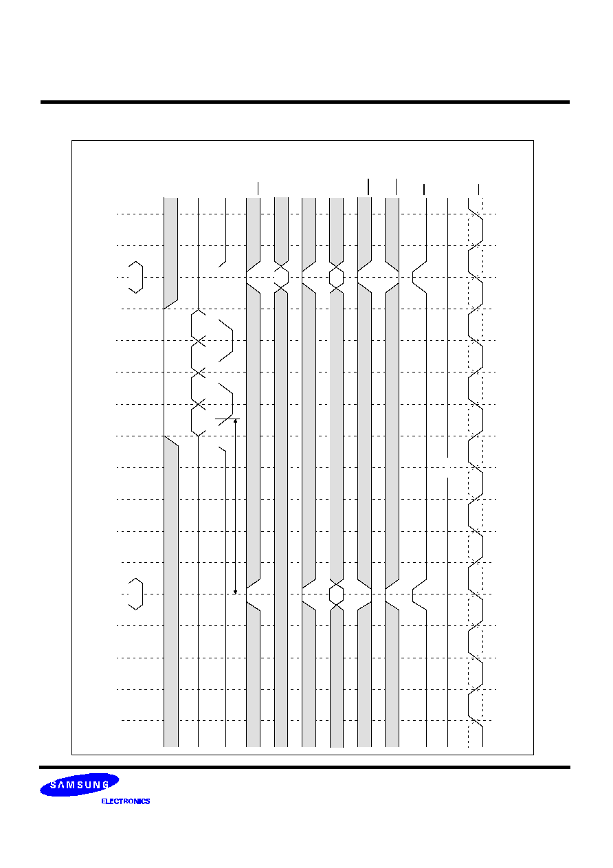
Preliminary
64M DDR SGRAM
K4D623237M
Normal WRITE Burst (@BL=4)
C
O
M
M
A
N
D
D
Q
S
D
Q
C
K
E
C
S
W
E
D
M
R
A
S
C
A
S
0
1
2
3
4
5
6
7
8
t
R
D
L
B
A
a
C
a
W
R
I
T
E
P
R
E
C
H
A
R
G
E
H
I
G
H
B
A
a
D
a
0
D
a
1
D
a
2
D
a
3
C
K
,
C
K
A
8
/
A
P
A
D
D
R
(
A
0
~
A
7
,
A
9
,
A
1
0
)
B
A
[
1
:
0
]

Preliminary
64M DDR SGRAM
K4D623237M
Write Interrupted by Precharge & DM (@BL=8)
C
O
M
M
A
N
D
D
Q
S
D
Q
C
K
E
C
S
W
E
D
M
R
A
S
C
A
S
0
1
2
3
4
5
6
7
8
W
R
I
T
E
P
R
E
W
R
I
T
E
W
R
I
T
E
t
R
D
L
t
C
C
D
B
A
a
B
A
b
C
a
C
b
C
H
A
R
G
E
H
I
G
H
B
A
c
C
c
B
A
a
D
a
0
D
a
1
D
a
2
D
a
3
D
a
4
D
a
5
D
a
6
D
a
7
D
b
0
D
b
1
D
c
0
D
c
1
D
c
2
C
K
,
C
K
A
8
/
A
P
A
D
D
R
(
A
0
~
A
7
,
A
9
,
A
1
0
)
B
A
[
1
:
0
]

Preliminary
64M DDR SGRAM
K4D623237M
Write Interrupted by a Read (@BL=8, CL=2)
C
O
M
M
A
N
D
D
Q
S
D
Q
C
K
E
C
S
W
E
D
M
R
A
S
C
A
S
0
1
2
3
4
5
6
7
8
W
R
I
T
E
R
E
A
D
t
C
D
L
R
M
a
s
k
e
d
b
y
D
Q
M
B
A
a
B
A
b
C
b
H
I
G
H
C
a
D
a
0
D
a
1
D
a
2
D
a
3
D
a
4
D
a
5
Q
b
0
Q
D
b
1
Q
b
2
Q
b
3
Q
b
4
C
K
,
C
K
A
8
/
A
P
A
D
D
R
(
A
0
~
A
7
,
A
9
,
A
1
0
)
B
A
[
1
:
0
]
Q
b
5

Preliminary
64M DDR SGRAM
K4D623237M
Read Interrupted by Precharge (@BL=8)
0
1
2
3
4
5
6
7
8
C
O
M
M
A
N
D
C
K
E
C
S
W
E
D
M
R
A
S
C
A
S
D
Q
S
(
C
L
=
3
)
D
Q
(
C
L
=
3
)
Q
a
0
Q
a
1
Q
a
2
Q
a
3
Q
a
4
Q
a
5
2
.
5
C
L
K
V
a
l
i
d
5
e
a
B
A
a
C
a
R
E
A
D
P
R
E
C
H
A
R
G
E
H
I
G
H
B
A
a
D
Q
S
(
C
L
=
2
)
D
Q
(
C
L
=
2
)
Q
a
0
Q
a
1
Q
a
2
Q
a
3
Q
a
4
Q
a
5
1
.
5
C
L
K
V
a
l
i
d
3
e
a
C
K
,
C
K
A
8
/
A
P
A
D
D
R
(
A
0
~
A
7
,
A
9
,
A
1
0
)
B
A
[
1
:
0
]

Preliminary
64M DDR SGRAM
K4D623237M
Read Interrupted by Burst stop & Write (@BL=8, CL=2)
C
O
M
M
A
N
D
D
Q
S
D
Q
C
K
E
C
S
W
E
D
M
R
A
S
C
A
S
0
1
2
3
4
5
6
7
8
R
E
A
D
W
R
I
T
E
Q
a
0
Q
a
1
B
A
a
C
a
H
I
G
H
B
A
b
C
b
B
u
r
s
t
S
t
o
p
Q
b
0
Q
D
b
1
Q
b
2
Q
b
3
Q
b
4
Q
b
5
Q
b
6
C
K
,
C
K
A
8
/
A
P
A
D
D
R
(
A
0
~
A
7
,
A
9
,
A
1
0
)
B
A
[
1
:
0
]
Q
b
7

Preliminary
64M DDR SGRAM
K4D623237M
Read Interrupted by a Read (@BL=8, CL=2)
D
Q
S
D
Q
C
K
E
C
S
W
E
D
M
R
A
S
C
A
S
0
1
2
3
4
5
6
7
8
Q
b
0
Q
b
1
Q
b
2
Q
b
3
Q
b
4
Q
b
5
Q
a
0
Q
a
1
Q
b
6
Q
b
7
t
C
C
D
C
O
M
M
A
N
D
B
A
a
B
A
b
C
a
C
b
R
E
A
D
R
E
A
D
H
I
G
H
C
K
,
C
K
A
8
/
A
P
A
D
D
R
(
A
0
~
A
7
,
A
9
,
A
1
0
)
B
A
[
1
:
0
]

Preliminary
64M DDR SGRAM
K4D623237M
DM Function (@BL=8) only for write
C
O
M
M
A
N
D
D
Q
S
(
C
L
=
2
)
D
Q
(
C
L
=
2
)
0
1
2
3
4
5
6
7
8
C
K
E
C
S
W
E
D
M
R
A
S
C
A
S
W
R
I
T
E
B
A
a
C
a
H
I
G
H
D
a
0
D
a
1
D
a
2
D
a
3
D
a
4
D
a
5
D
a
6
D
a
7
C
K
,
C
K
A
8
/
A
P
A
D
D
R
(
A
0
~
A
7
,
A
9
,
A
1
0
)
B
A
[
1
:
0
]

Preliminary
64M DDR SGRAM
K4D623237M
Power up Sequence & Auto Refresh(CBR)
D
Q
S
D
Q
0
1
2
3
4
5
6
7
8
C
K
E
C
S
W
E
D
M
R
A
S
C
A
S
H
I
G
H
C
K
,
C
K
A
8
/
A
P
A
D
D
R
(
A
0
~
A
7
,
A
9
,
A
1
0
)
H
i
g
h
-
Z
P
r
e
c
h
a
r
g
e
1
s
t
A
u
t
o
R
e
f
r
e
s
h
M
o
d
e
R
e
s
i
s
t
e
r
S
e
t
C
o
m
m
a
n
d
t
R
C
H
i
g
h
-
Z
A
D
D
R
E
S
S
K
E
Y
A
l
l
B
a
n
k
C
o
m
m
a
n
d
2
n
d
A
u
t
o
R
e
f
r
e
s
h
C
o
m
m
a
n
d
C
o
m
m
a
n
d
A
n
y
C
o
m
m
a
n
d
M
i
n
i
m
u
m
o
f
2
R
e
f
r
e
s
h
C
y
c
l
e
s
a
r
e
r
e
q
u
i
r
e
d
I
n
p
u
t
s
m
u
s
t
b
e
s
t
a
b
l
e
f
o
r
2
0
0
u
s
t
R
C
B
A
[
1
:
0
]
H
I
G
H
t
R
P
t
M
R
D

Preliminary
64M DDR SGRAM
K4D623237M
Mode Register Set
D
Q
S
(
C
L
=
2
)
D
Q
(
C
L
=
2
)
0
1
2
3
4
5
6
7
8
C
K
E
C
S
W
E
D
M
R
A
S
C
A
S
H
I
G
H
C
K
,
C
K
A
8
/
A
P
A
D
D
R
(
A
0
~
A
7
,
A
9
,
A
1
0
)
P
r
e
c
h
a
r
g
e
M
o
d
e
R
e
s
i
s
t
e
r
S
e
t
C
o
m
m
a
n
d
H
i
g
h
-
Z
A
l
l
B
a
n
k
C
o
m
m
a
n
d
A
n
y
C
o
m
m
a
n
d
t
R
P
H
i
g
h
-
Z
H
i
g
h
-
Z
A
D
D
R
E
S
S
K
E
Y
B
A
[
1
:
0
]
t
M
R
D
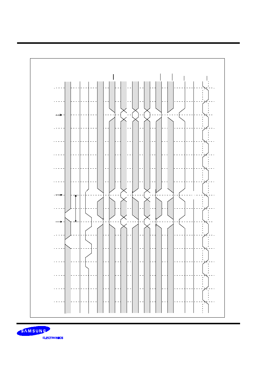
Preliminary
64M DDR SGRAM
K4D623237M
Block Write cycle (with Auto Precharge)
D
S
F
D
M
0
1
2
3
4
5
6
7
8
C
K
E
C
S
W
E
D
Q
R
A
S
C
A
S
H
I
G
H
C
K
,
C
K
A
8
/
A
P
A
D
D
R
(
A
0
~
A
7
,
A
9
,
A
1
0
)
R
o
w
A
c
t
i
v
e
(
A
-
B
a
n
k
)
B
l
o
c
k
W
r
i
t
e
(
A
-
B
a
n
k
)
B
l
o
c
k
W
r
i
t
e
w
i
t
h
A
u
t
o
P
r
e
c
h
a
r
g
e
(
A
-
B
a
n
k
)
*
N
o
t
e
:
1
.
A
t
B
l
o
c
k
W
r
i
t
e
,
C
A
0
~
3
a
r
e
i
g
n
o
r
e
d
.
D
Q
S
B
A
a
R
A
a
R
A
a
B
A
b
C
A
b
B
A
a
C
A
b
B
A
[
1
:
0
]
t
B
W
C
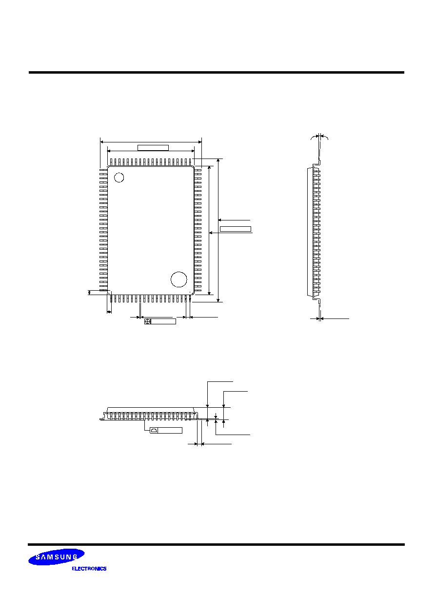
Preliminary
64M DDR SGRAM
K4D623237M
0.825
0
.
5
7
5
0.65
0.13 MAX
PACKAGE DIMENSIONS (TQFP)
Dimensions in Millimeters
0.10 MAX
0 ~ 7
∞
17.20
±
0.20
14.00
±
0.10
23.20
±
0.20
1.00
±
0.10
1.20 MAX *
0.05 MIN
0.80
±
0.20
#1
0.09~0.20
#100
0.30
±
0.08
20.00
±
0.10