
DRAM MODULE
M364E040(8)4BT0-C
Buffered 4Mx64 DIMM
Revision 0.1
June 1998
(4Mx16 base)

DRAM MODULE
M364E040(8)4BT0-C
Revision History
Version 0.0 (Sept. 1997)
∑ Removed two AC parameters t
CACP
(access time from CAS) and t
AAP
(access time from col. addr.) in AC CHARACTERISTICS.
∑ Changed the parameter t
CAC
(access time from CAS) from 18ns to 20ns @ -5 in AC CHARACTERISTICS.
Version 0.1 (June 1998)
∑ The 3rd. generation of 64 DRAM components are applied for this module.

DRAM MODULE
M364E040(8)4BT0-C
M364E040(8)4BT0-C EDO Mode
4M x 64 DRAM DIMM Using 4Mx16, 4K & 8K Refresh, 5V
The Samsung M364E040(8)4BT0-C is a 4Mx64bits Dynamic
RAM high density memory module. The Samsung
M364E040(8)4BT0-C consists of four CMOS 4Mx16bits
DRAMs in TSOP-II 400mil packages and two 16 bits driver IC
in TSSOP package mounted on a 168-pin glass-epoxy sub-
strate. A 0.1 or 0.22uF decoupling capacitor is mounted on
the printed circuit board for each DRAM. The
M364E040(8)4BT0-C is a Dual In-line Memory Module and is
intended for mounting into 168 pin edge connector sockets.
GENERAL DESCRIPTION
PD Note :PD & ID Terminals must each be pulled up through a resistor to V
CC
at the next higher
level assembly. PDs will be either open (NC) or driven to V
SS
via on-board buffer circuits.
ID Note : IDs will be either open (NC) or connected directly to V
SS
without a buffer.
FEATURES
∑ Part Identification
∑ Extended Data Out Mode Operation
∑ CAS-before-RAS Refresh capability
∑ RAS-only and Hidden refresh capability
∑ TTL compatible inputs and outputs
∑ Single 5V
±
10% power supply
∑ JEDEC standard pinout & Buffered PDpin
∑ Buffered input except RAS and DQ
∑ PCB : Height(1000mil), single sided component
Part number
PKG
Ref.
CBR Ref.
ROR Ref.
M364E0404BT0-C
TSOPll
4K
4K/64ms
M364E0484BT0-C
TSOPll
8K
4K/64ms
8K/64ms
PIN NAMES
Pins marked
*
are not used in this module.
Pin Names
Function
A0, B0, A1 - A11
Address Input(4K ref.)
A0, B0, A1 - A12
Address Input(8K ref.)
DQ0 - DQ71
Data In/Out
W0, W2
Read/Write Enable
OE0, OE2
Output Enable
RAS0, RAS2
Row Address Strobe
CAS0 - CAS7
Column Address Strobe
V
CC
Power(+5V)
V
SS
Ground
NC
No Connection
PDE
Presence Detect Enable
PD1 - 8
Presence Detect
ID0 - 1
ID bit
RSVD
Reserved Use
RFU
Reserved for Future Use
PD & ID Table
PD : 0 for Vol of Drive IC & 1 for N.C
ID : 0 for Vss & 1 for N.C
Pin
50NS
60NS
PD1
PD2
PD3
PD4
PD5
PD6
PD7
PD8
1
1
0
1
1
0
0
1
1
1
0
1
1
1
1
1
ID0
ID1
0
0
0
0
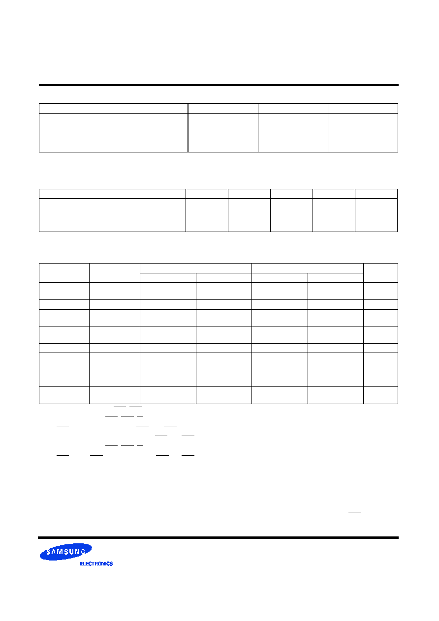
PIN CONFIGURATIONS
NOTE : A12 is used for only M364E0484BT0-C (8K Ref.)
Pin
1
2
3
4
5
6
7
8
9
10
11
12
13
14
15
16
17
18
19
20
21
22
23
24
25
26
27
28
Front
V
SS
DQ0
DQ1
DQ2
DQ3
V
CC
DQ4
DQ5
DQ6
DQ7
*DQ8
V
SS
DQ9
DQ10
DQ11
DQ12
DQ13
V
CC
DQ14
DQ15
DQ16
*DQ17
V
SS
RSVD
RSVD
V
CC
W0
CAS0
Pin
29
30
31
32
33
34
35
36
37
38
39
40
41
42
43
44
45
46
47
48
49
50
51
52
53
54
55
56
Front
CAS2
RAS0
OE0
V
SS
A0
A2
A4
A6
A8
A10
A12
V
CC
RFU
RFU
V
SS
OE2
RAS2
CAS4
CAS6
W2
V
CC
RSVD
RSVD
DQ18
DQ19
V
SS
DQ20
DQ21
Pin
57
58
59
60
61
62
63
64
65
66
67
68
69
70
71
72
73
74
75
76
77
78
79
80
81
82
83
84
Front
DQ22
DQ23
V
CC
DQ24
RFU
RFU
RFU
RFU
DQ25
*DQ26
DQ27
V
SS
DQ28
DQ29
DQ30
DQ31
V
CC
DQ32
DQ33
DQ34
*DQ35
V
SS
PD1
PD3
PD5
PD7
ID0
V
CC
Pin
85
86
87
88
89
90
91
92
93
94
95
96
97
98
99
100
101
102
103
104
105
106
107
108
109
110
111
112
Back
V
SS
DQ36
DQ37
DQ38
DQ39
V
CC
DQ40
DQ41
DQ42
DQ43
*DQ44
V
SS
DQ45
DQ46
DQ47
DQ48
DQ49
V
CC
DQ50
DQ51
DQ52
*DQ53
V
SS
RSVD
RSVD
V
CC
RFU
CAS1
Pin
113
114
115
116
117
118
119
120
121
122
123
124
125
126
127
128
129
130
131
132
133
134
135
136
137
138
139
140
Back
CAS3
*RAS1
RFU
V
SS
A1
A3
A5
A7
A9
A11
*A13
V
CC
RFU
B0
V
SS
RFU
*RAS3
CAS5
CAS7
PDE
V
CC
RSVD
RSVD
DQ54
DQ55
V
SS
DQ56
DQ57
Pin
141
142
143
144
145
146
147
148
149
150
151
152
153
154
155
156
157
158
159
160
161
162
163
164
165
166
167
168
Back
DQ58
DQ59
V
CC
DQ60
RFU
RFU
RFU
RFU
DQ61
*DQ62
DQ63
V
SS
DQ64
DQ65
DQ66
DQ67
V
CC
DQ68
DQ69
DQ70
*DQ71
V
SS
PD2
PD4
PD6
PD8
ID1
V
CC
c
PERFORMANCE RANGE
Speed
t
RAC
t
CAC
t
RC
t
HPC
-C50
50ns
18ns
84ns
20ns
-C60
60ns
20ns
104ns
25ns
DRAM MODULE
M364E040(8)4BT0-C
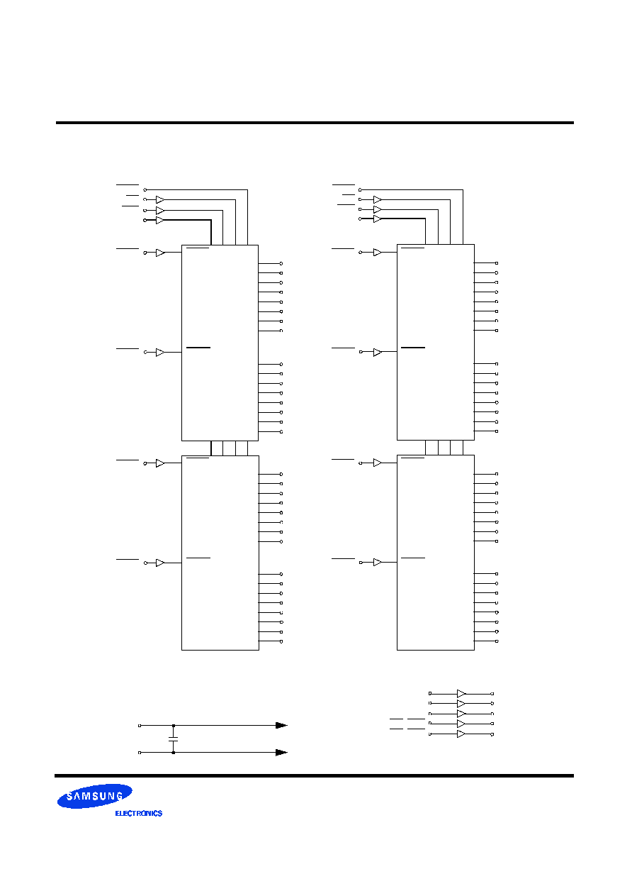
FUNCTIONAL BLOCK DIAGRAM
Vcc
Vss
0.1 or 0.22uF Capacitor
under each DRAM
To all DRAMs
A0
B0
A1-A11(A12)
W0, OE0
W2, OE2
U0-U1
U2-U3
U0-U3
U0-U1
U2-U3
RAS0
W0
OE0
A0
CAS1
DQ0
DQ1
DQ2
DQ3
DQ4
DQ5
DQ6
DQ7
DQ8
DQ9
DQ10
DQ11
DQ12
DQ13
DQ14
DQ15
U0
DQ0
DQ1
DQ2
DQ3
DQ4
DQ5
DQ6
DQ7
DQ9
DQ10
DQ11
DQ12
DQ13
DQ14
DQ15
DQ16
CAS2
CAS3
U1
DQ18
DQ19
DQ20
DQ21
DQ22
DQ23
DQ24
DQ25
DQ27
DQ28
DQ29
DQ30
DQ31
DQ32
DQ33
DQ34
CAS4
CAS5
U2
DQ36
DQ37
DQ38
DQ39
DQ40
DQ41
DQ42
DQ43
DQ45
DQ46
DQ47
DQ48
DQ49
DQ50
DQ51
DQ52
CAS6
CAS7
U3
DQ54
DQ55
DQ56
DQ57
DQ58
DQ59
DQ60
DQ61
DQ63
DQ64
DQ65
DQ66
DQ67
DQ68
DQ69
DQ70
RAS2
W2
OE2
CAS0
DQ0
DQ1
DQ2
DQ3
DQ4
DQ5
DQ6
DQ7
DQ8
DQ9
DQ10
DQ11
DQ12
DQ13
DQ14
DQ15
DQ0
DQ1
DQ2
DQ3
DQ4
DQ5
DQ6
DQ7
DQ8
DQ9
DQ10
DQ11
DQ12
DQ13
DQ14
DQ15
DQ0
DQ1
DQ2
DQ3
DQ4
DQ5
DQ6
DQ7
DQ8
DQ9
DQ10
DQ11
DQ12
DQ13
DQ14
DQ15
A1-A11(A12)
B0
A1-A11(A12)
Note : A12 is used for only M364E0484BT0 (8K ref.)
UCAS
LCAS
UCAS
LCAS
UCAS
LCAS
UCAS
LCAS
DRAM MODULE
M364E040(8)4BT0-C
* NOTE : I
CC1
, I
CC3
, I
CC4
and I
CC6
are dependent on output loading and cycle rates. Specified values are obtained with the output open.
I
CC
is specified as an average current. In I
CC1
and I
CC3
, address can be changed maximum once while RAS=V
IL
. In I
CC4
,
address can be changed maximum once within one EDO mode cycle time,
t
HPC
.
ABSOLUTE MAXIMUM RATINGS *
* Permanent device damage may occur if ABSOLUTE MAXIMUM RATINGS are exceeded. Functional operation should be restricted to
the conditions as detailed in the operational sections of this data sheet. Exposure to absolute maximum rating conditions for intended
periods may affect device reliability.
Item
Symbol
Rating
Unit
Voltage on any pin relative V
SS
Voltage on V
CC
supply relative to V
SS
Storage Temperature
Power Dissipation
Short Circuit Output Current
V
IN
, V
OUT
V
CC
T
stg
P
D
I
OS
-1 to +7.0
-1 to +7.0
-55 to +125
4
50
V
V
∞
C
W
mA
RECOMMENDED OPERATING CONDITIONS
(Voltage referenced to V
SS
, T
A
= 0 to 70
∞
C)
*1 : V
CC
+2.0V at pulse width
20ns, which is measured at V
CC
.
*2 : -2.0V at pulse width
20ns, which is measured at V
SS
.
Item
Symbol
Min
Typ
Max
Unit
Supply Voltage
Ground
Input High Voltage
Input Low Voltage
V
CC
V
SS
V
IH
V
IL
4.5
0
2.4
-1.0
*2
5.0
0
-
-
5.5
0
V
CC
*1
0.8
V
V
V
V
DC AND OPERATING CHARACTERISTICS
(Recommended operating conditions unless otherwise noted)
I
CC1
*
I
CC2
I
CC3
*
I
CC4
*
I
CC5
I
CC6
*
I(
IL)
I(
OL)
V
OH
V
OL
Symbol
Speed
M364E0404BT0
M364E0484BT0
Unit
Min
Max
Min
Max
I
CC1
-50
-60
-
-
480
440
-
-
360
320
mA
mA
I
CC2
Don
t care
-
100
-
100
mA
I
CC3
-50
-60
-
-
480
440
-
-
360
320
mA
mA
I
CC4
-50
-60
-
-
440
400
-
-
400
360
mA
mA
I
CC5
Don
t care
-
30
-
30
mA
I
CC6
-50
-60
-
-
480
440
-
-
360
320
mA
mA
I
I(L)
I
O(L)
Don
t care
-10
-5
10
5
-10
-5
10
5
uA
uA
V
OH
V
OL
Don
t care
2.4
-
-
0.4
2.4
-
-
0.4
V
V
: Operating Current * (RAS, CAS, Address cycling @
t
RC
=min)
: Standby Current (RAS=CAS=W=V
IH
)
: RAS Only Refresh Current * (CAS=V
IH
, RAS cycling @
t
RC
=min)
: Extended Data Out Mode Current * (RAS=V
IL
, CAS cycling :
t
HPC
=min)
: Standby Current (RAS=CAS=W=Vcc-0.2V)
: CAS-Before-RAS Refresh Current * (RAS and CAS cycling @
t
RC
=min)
: Input Leakage Current (Any input 0
V
IN
Vcc+0.5V, all other pins not under test=0 V)
: Output Leakage Current(Data Out is disabled, 0V
V
OUT
Vcc)
: Output High Voltage Level (I
OH
= -5mA)
: Output Low Voltage Level (I
OL
= 4.2mA)

DRAM MODULE
M364E040(8)4BT0-C
CAPACITANCE
(T
A
= 25
∞
C, f = 1MHz)
Item
Symbol
Min
Max
Unit
Input capacitance[A0, B0, A1 - A12]
Input capacitance[W0, W2, OE0, OE2]
Input capacitance[RAS0, RAS2]
Input capacitance[CAS0 - CAS7]
Input/Output capacitance[DQ0 - 71]
C
IN1
C
IN2
C
IN3
C
IN4
C
DQ
-
-
-
-
-
20
20
24
20
17
pF
pF
pF
pF
pF
AC CHARACTERISTICS
(0
∞
C
T
A
70
∞
C, V
CC
=5.0V
±
10%. See notes 1,2.)
Test condition : V
ih
/V
il
=2.6/0.8V, V
oh
/V
ol
=2.0/0.8V, output loading CL=100pF
Parameter
Symbol
-50
-60
Unit
Note
Min
Max
Min
Max
Random read or write cycle time
t
RC
84
104
ns
Read-modify-write cycle time
t
RWC
133
155
ns
Access time from RAS
t
RAC
50
60
ns
Access time from CAS
t
CAC
18
20
ns
3,4,5,13
Access time from column address
t
AA
30
35
ns
3,10,13
CAS to output in Low-Z
t
CLZ
8
8
ns
3,13
OE to output in Low-Z
t
OLZ
8
8
ns
3,13
Output buffer turn-off delay from CAS
t
CEZ
8
18
8
18
ns
6,11,13
Transition time(rise and fall)
t
T
1
50
1
50
ns
2
RAS precharge time
t
RP
30
40
ns
RAS pulse width
t
RAS
50
10K
60
10K
ns
RAS hold time
t
RSH
18
20
ns
13
CAS hold time
t
CSH
36
43
ns
13
CAS pulse width
t
CAS
8
10K
10
10K
ns
RAS to CAS delay time
t
RCD
18
32
18
40
ns
4,13
RAS to column address delay time
t
RAD
13
20
13
25
ns
10,13
CAS to RAS precharge time
t
CRP
10
10
ns
13
Row address set-up time
t
ASR
5
5
ns
13
Row address hold time
t
RAH
8
8
ns
13
Column address set-up time
t
ASC
0
0
ns
14
Column address hold time
t
CAH
8
10
ns
14
Column address to RAS lead time
t
RAL
30
35
ns
13
Read command set-up time
t
RCS
0
0
ns
Read command hold referenced to CAS
t
RCH
0
0
ns
8
Read command hold referenced to RAS
t
RRH
-2
-2
ns
8,13
Write command set-up time
t
WCS
0
0
ns
7
Write command hold time
t
WCH
10
10
ns
Write command pulse width
t
WP
10
10
ns
Write command to RAS lead time
t
RWL
18
20
ns
13
Write command to CAS lead time
t
CWL
8
10
ns
17
Data set-up time
t
DS
-2
-2
ns
9,13
Data hold time
t
DH
13
15
ns
9,13
Refresh period(4K & 8K)
t
REF
64
64
ms
CAS to W delay time
t
CWD
36
38
ns
7,16
RAS to W delay time
t
RWD
73
83
ns
7,13
DRAM MODULE
M364E040(8)4BT0-C
AC CHARACTERISTICS
(0
∞
C
T
A
70
∞
C, V
CC
=5.0V
±
10%. See notes 1,2.)
Parameter
Symbol
-50
-60
Unit
Note
Min
Max
Min
Max
Column address to W delay time
t
AWD
48
53
ns
7
CAS precharge time to W delay time
t
CPWD
53
60
ns
CAS setup time(CAS-before-RAS refresh)
t
CSR
10
10
ns
13,18
CAS hold time(CAS-before-RAS refresh)
t
CHR
8
8
ns
13
RAS to CAS precharge time
t
RPC
3
3
ns
13
Access time from CAS precharge
t
CPA
33
40
ns
3,13
Hyper page cycle time
t
HPC
20
25
ns
12
Hyper page read-modify-write cycle time
t
HPRWC
70
77
ns
12
CAS precharge time(Hyper page cycle)
t
CP
8
10
ns
15
RAS pulse width (Hyper page cycle)
t
RASP
50
200K
60
200K
ns
RAS hold time from CAS precharge
t
RHCP
35
40
ns
13
W to RAS precharge time(C-B-R refresh)
t
WRP
15
15
ns
13
W to RAS hold time(C-B-R refresh)
t
WRH
8
8
ns
13
OE access time
t
OEA
18
20
ns
13
OE to data delay
t
OED
18
18
ns
13
Output buffer turn off delay time from OE
t
OEZ
8
18
8
18
ns
13
OE command hold time
t
OEH
13
15
ns
Output data hold time(C-B-R refresh)
t
DOH
10
10
ns
13
Output buffer turn off delay time from RAS
t
REZ
3
15
3
15
ns
6,11
Output buffer turn off delay time from W
t
WEZ
8
18
8
20
ns
6,13
W to data delay
t
WED
20
20
ns
13
OE to CAS hold time
t
OCH
5
5
ns
CAS hold time to OE
t
CHO
5
5
ns
OE precharge time
t
OEP
5
5
ns
W pulse width (Hyper page cycle)
t
WPE
5
5
ns
PDE to Valid PD bit
t
PD
10
10
ns
PDE to PD bit Inactive
t
PDOFF
2
7
2
7
ns
Present Detect Read Cycle

DRAM MODULE
M364E040(8)4BT0-C
NOTES
An initial pause of 200us is required after power-up followed
by any 8 RAS-only or CAS-before-RAS refresh cycles before
proper device operation is achieved.
Input voltage levels are V
ih
/V
il
. V
IH
(min) and V
IL
(max) are ref-
erence levels for measuring timing of input signals. Transition
times are measured between V
IH
(min) and V
IL
(max) and are
assumed to be 5ns for all inputs.
Measured with a load equivalent to 2 TTL loads and 100pF.
Operation within the
t
RCD
(max) limit insures that
t
RAC
(max)
can be met.
t
RCD
(max) is specified as a reference point only.
If
t
RCD
is greater than the specified
t
RCD
(max) limit, then
access time is controlled exclusively by
t
CAC
.
Assumes that
t
RCD
t
RCD
(max).
This parameter defines the time at which the output achieves
the open circuit condition and is not referenced to V
OH
or
V
OL
.
t
WCS
,
t
RWD
,
t
CWD
,
t
AWD
and
t
CPWD
are not restrictive operat-
ing parameter. They are included in the data sheet as electri-
cal characteristics only. If
t
WCS
t
WCS
(min) the cycle is an
early write cycle and the data out pin will remain high imped-
ance for the duration of the cycle. If
t
RWD
t
RWD
(min),
t
CWD
t
CWD
(min),
t
AWD
t
AWD
(min) and
t
CPWD
t
CPWD
(min).
The cycle is a read-modify-write cycle and the data out will
contain data read from the selected cell. If neither of the
above sets of conditions is satisfied, the condition of data
out(at access time) is indeterminate.
Either
t
RCH
or
t
RRH
must be satisfied for a read cycle.
These parameters are referenced to the CAS leading edge in
early write cycles.
Operation within the
t
RAD
(max) limit insures that
t
RAC
(max)
can be met.
t
RAD
(max) is specified as reference point only. If
t
RAD
is greater than the specified
t
RAD
(max) limit, then
access time is controlled by
t
AA
.
If RAS goes high before CAS high going, the open circuit
condition of the output is achieved by CAS high going. If CAS
goes high before RAS high going , the open circuit condition
of the output is achieved by RAS going.
t
ASC
6ns.
The timing skew from the DRAM to the DIMM resulted from
the addition of buffers.
t
ASC
,
t
CAH
are referenced to the earlier CAS falling edge.
t
CP
is specified from the last CAS rising edge in the previous
cycle to the first CAS falling edge in the next cycle.
t
CWD
is referenced to the later CAS falling edge at word read-
modify-write cycle.
t
CWL
is specified from W falling edge to the earlier CAS rising
edge.
t
CSR
is referenced to earlier CAS falling low before RAS tran-
sition low.
1.
2.
3.
4.
5.
6.
7.
8.
9.
10.
12.
13.
11.
14.
15.
16.
17.
18.
DRAM MODULE
M364E040(8)4BT0-C
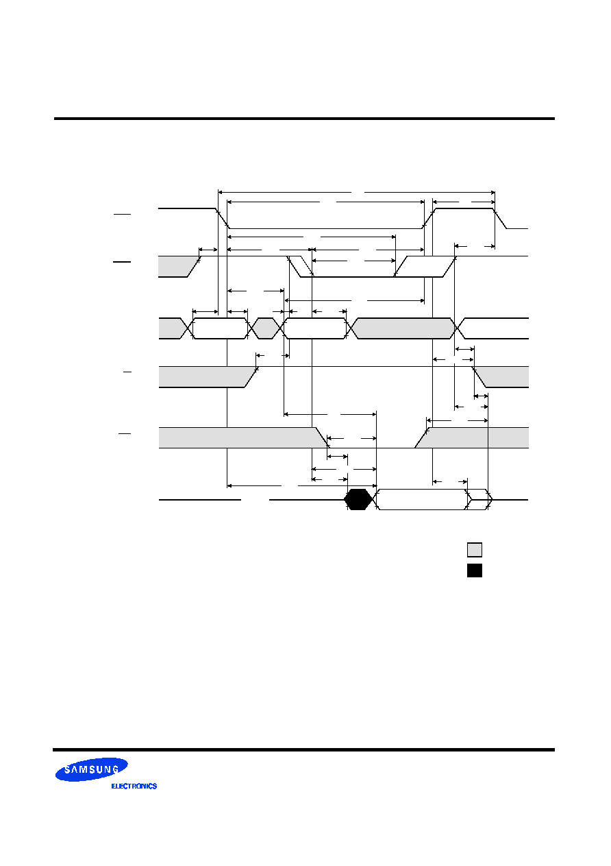
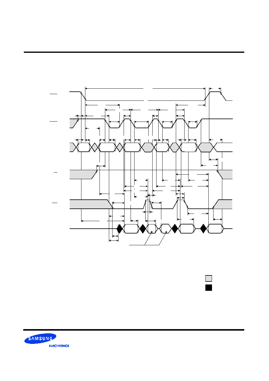
RAS
V
IH
-
V
IL
-
CAS
V
IH
-
V
IL
-
A
V
IH
-
V
IL
-
W
V
IH
-
V
IL
-
OE
V
IH
-
V
IL
-
V
OH
-
V
OL
-
COLUMN
ADDRESS
ROW
ADDRESS
t
RAS
t
RC
t
CRP
t
RP
t
CSH
t
RSH
t
RCD
t
CAS
t
RAL
t
ASR
t
RAH
t
ASC
t
CAH
t
CRP
t
AA
t
OEA
t
CLZ
t
RAC
OPEN
t
RCH
Don
t care
Undefined
t
RAD
t
RRH
DATA-OUT
t
REZ
t
RCS
READ CYCLE
t
OEZ
t
CEZ
t
WEZ
DQ
t
OLZ
t
CAC

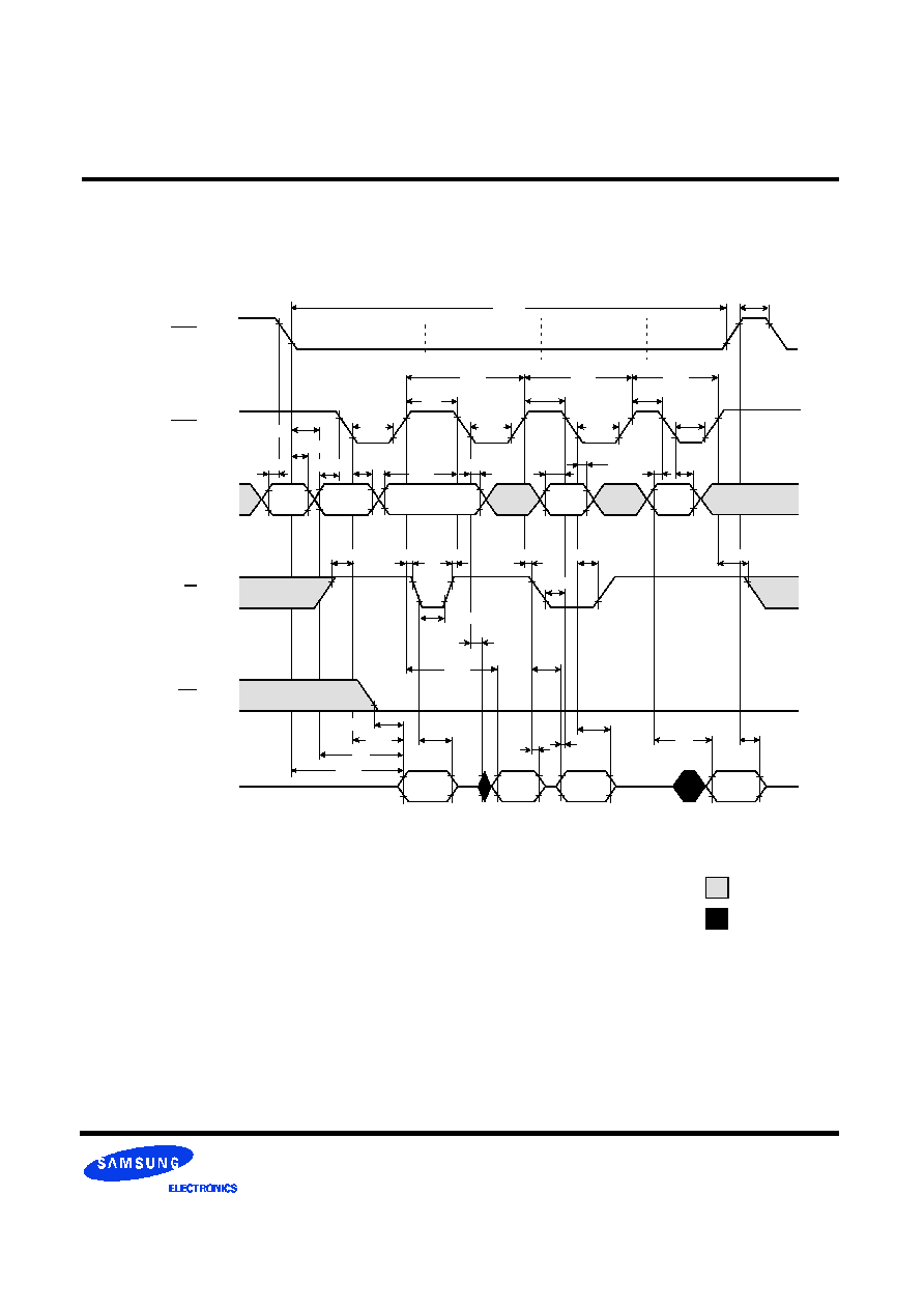
DRAM MODULE
M364E040(8)4BT0-C
t
WCS
NOTE : D
OUT
= OPEN
WRITE CYCLE ( EARLY WRITE )
RAS
V
IH
-
V
IL
-
V
IH
-
V
IL
-
A
V
IH
-
V
IL
-
W
V
IH
-
V
IL
-
OE
V
IH
-
V
IL
-
V
IH
-
V
IL
-
COLUMN
ADDRESS
ROW
ADDRESS
t
RAS
t
RC
t
CRP
t
RP
t
CSH
t
RSH
t
RCD
t
CAS
t
RAL
t
RAD
t
ASR
t
RAH
t
ASC
t
CAH
t
CRP
Don
t care
Undefined
t
WCH
t
WP
CAS
t
RWL
t
CWL
t
DS
t
DH
DATA-IN
DQ

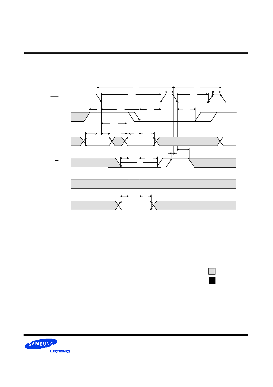
DRAM MODULE
M364E040(8)4BT0-C
NOTE : D
OUT
= OPEN
WRITE CYCLE ( OE CONTROLLED WRITE )
RAS
V
IH
-
V
IL
-
A
V
IH
-
V
IL
-
W
V
IH
-
V
IL
-
OE
V
IH
-
V
IL
-
V
IH
-
V
IL
-
DQ
COLUMN
ADDRESS
ROW
ADDRESS
t
RAS
t
RC
t
CRP
t
RP
t
CSH
t
RSH
t
RCD
t
CAS
t
RAL
t
RAD
t
ASR
t
RAH
t
ASC
t
CAH
t
CRP
t
WP
Don
t care
Undefined
CAS
V
IH
-
V
IL
-
t
RWL
t
CWL
t
DH
t
OEH
t
OED
DATA-IN
t
DS

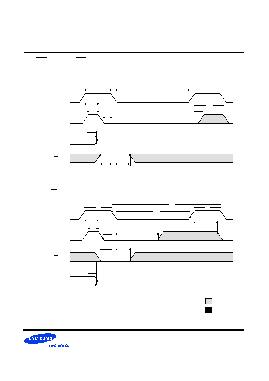
DRAM MODULE
M364E040(8)4BT0-C
READ - MODIFY - WRITE CYCLE
RAS
V
IH
-
V
IL
-
CAS
V
IH
-
V
IL
-
A
V
IH
-
V
IL
-
W
V
IH
-
V
IL
-
OE
V
IH
-
V
IL
-
V
I/OH
-
V
I/OL
-
DQ
ROW
ADDR
t
RAS
t
RWC
t
RP
t
RSH
t
RCD
t
CAS
t
CSH
t
RAD
t
ASR
t
RAH
t
ASC
t
CAH
t
CRP
VALID
t
WP
Don
t care
t
RWL
t
CWL
t
OEZ
t
OEA
t
OED
t
AWD
t
CWD
t
RWD
DATA-OUT
Undefined
VALID
DATA-IN
t
RAC
t
AA
t
CAC
t
CLZ
t
DS
t
DH
COLUMN
ADDRESS
t
OLZ
DRAM MODULE
M364E040(8)4BT0-C
t
DOH
HYPER PAGE READ CYCLE
RAS
V
IH
-
V
IL
-
CAS
V
IH
-
V
IL
-
A
V
IH
-
V
IL
-
W
V
IH
-
V
IL
-
OE
V
IH
-
V
IL
-
COLUMN
ADDRESS
ROW
ADDR
t
RASP
t
RP
t
RCD
t
ASR
t
CRP
Don
t care
Undefined
V
OH
-
V
OL
-
DQ
t
OEP
COLUMN
ADDRESS
t
CAS
t
CAS
t
CAS
t
CAS
t
CP
t
CP
t
CP
t
HPC
t
HPC
t
HPC
t
RHCP
t
CSH
t
RAD
t
RAH
t
ASC
t
CAH
t
CAH
t
CAH
t
ASC
t
CAH
t
RCS
t
AA
t
RCH
t
ASC
COLUMN
ADDRESS
COLUMN
ADDR
VALID
DATA-OUT
t
OEZ
t
OEA
t
OEP
t
AA
t
CAC
t
OEA
t
AA
t
CPA
t
CAC
t
CPA
VALID
DATA-OUT
VALID
DATA-OUT
t
OEZ
t
CLZ
t
RAC
t
OEA
t
OLZ
t
CAC
t
RRH
t
CHO
t
REZ
t
OEZ
t
CAC
t
OCH
t
CPA
t
CAC
VALID
DATA-OUT
°Û
t
ASC
t
AA

DRAM MODULE
M364E040(8)4BT0-C
RAS
V
IH
-
V
IL
-
CAS
V
IH
-
V
IL
-
A
V
IH
-
V
IL
-
W
V
IH
-
V
IL
-
OE
V
IH
-
V
IL
-
COLUMN
ADDRESS
ROW
ADDR.
t
RASP
t
RP
t
RCD
t
ASR
t
CRP
Don
t care
HYPER PAGE WRITE CYCLE ( EARLY WRITE )
Undefined
V
IH
-
V
IL
-
DQ
t
RHCP
t
RAD
t
RAH
t
CAH
t
CAH
t
ASC
t
CAH
t
ASC
VALID
DATA-IN
t
DS
°Û
COLUMN
ADDRESS
COLUMN
ADDRESS
t
CAS
t
CP
t
CAS
t
CP
t
CAS
t
RSH
°Û
t
CSH
t
ASC
°Û
°Û
t
WP
t
WCS
t
WCH
t
WP
t
WCS
t
WCH
t
WP
t
WCS
t
WCH
°Û
°Û
°Û
VALID
DATA-IN
VALID
DATA-IN
°Û
°Û
t
DH
t
DS
t
DH
t
DS
t
DH
t
CWL
t
CWL
t
CWL
t
RWL
NOTE : D
OUT
= OPEN
t
HPC
t
HPC

DRAM MODULE
M364E040(8)4BT0-C
Don
t care
HYPER PAGE READ-MODIFY-WRITE CYCLE
Undefined
RAS
V
IH
-
V
IL
-
CAS
V
IH
-
V
IL
-
A
V
IH
-
V
IL
-
W
V
IH
-
V
IL
-
OE
V
IH
-
V
IL
-
V
I/OH
-
V
I/OL
-
ROW
ADDR
t
CSH
t
RASP
t
RP
t
ASR
t
RAH
t
RCD
t
CP
t
RAD
t
CAH
t
WP
t
DH
COL.
ADDR
COL.
ADDR
t
CAS
t
CAS
t
CRP
t
ASC
t
CAH
t
RAL
t
RCS
t
CWL
t
CWD
t
AWD
t
RWD
t
WP
t
CWD
t
AWD
t
CWL
t
RAC
t
OEA
t
CLZ
t
OEZ
t
CPWD
t
OED
t
ASC
t
CLZ
t
OEA
t
CAC
t
AA
t
DH
t
OED
t
RWL
t
CRP
t
DS
t
OEZ
VALID
DATA-OUT
VALID
DATA-IN
VALID
DATA-OUT
VALID
DATA-IN
t
DS
DQ
t
RSH
t
OLZ
t
OLZ
t
HPRWC
t
CAC
t
AA
DRAM MODULE
M364E040(8)4BT0-C
HYPER PAGE READ AND WRITE MIXED CYCLE
RAS
V
IH
-
V
IL
-
CAS
V
IH
-
V
IL
-
A
V
IH
-
V
IL
-
W
V
IH
-
V
IL
-
OE
V
IH
-
V
IL
-
COLUMN
ADDRESS
ROW
ADDR
t
RASP
t
RP
Don
t care
Undefined
V
I/OH
-
V
I/OL
-
DQ
t
WEZ
t
CP
t
CP
t
HPC
t
HPC
t
HPC
t
RAD
t
RAH
t
ASC
t
CAH
t
CAH
t
CAH
t
ASC
t
CAH
t
RCH
t
RCS
t
RCS
t
RCH
t
ASC
COLUMN
ADDRESS
COL.
ADDR
VALID
DATA-OUT
t
REZ
t
AA
t
WCS
VALID
DATA-OUT
VALID
DATA-OUT
VALID
DATA-IN
t
RAC
COL.
ADDR
t
CAS
t
ASR
t
CAS
t
CAS
t
CAS
t
ASC
t
CP
t
RCH
t
WCH
t
WPE
t
CLZ
t
CPA
t
WED
t
AA
t
WEZ
t
DS
t
DH
t
CAC
t
OEA
READ(
t
CAC
)
READ(
t
CPA
)
WRITE
READ(
t
AA
)

DRAM MODULE
M364E040(8)4BT0-C
Don
t care
RAS - ONLY REFRESH CYCLE*
NOTE : W, OE, D
IN
= Don
t care
Undefined
D
OUT
= OPEN
RAS
V
IH
-
V
IL
-
CAS
V
IH
-
V
IL
-
A
V
IH
-
V
IL
-
ROW
ADDR
t
RC
t
RP
t
ASR
t
CRP
t
RAS
t
RAH
t
RPC
t
CRP
OPEN
CAS - BEFORE - RAS REFRESH CYCLE
NOTE : OE , A = Don
t care
RAS
V
IH
-
V
IL
-
CAS
V
IH
-
V
IL
-
t
RC
t
RP
t
RAS
t
RPC
t
CP
t
RPC
t
CSR
t
CHR
t
CEZ
V
OH
-
V
OL
-
DQ
t
WRP
t
WRH
W
V
IH
-
V
IL
-
t
RP
* In RAS-only refresh cycle of 64Mb A-dile & B-die, when CAS signal transits from Low to High, the valid data may be cut off.

DRAM MODULE
M364E040(8)4BT0-C
HIDDEN REFRESH CYCLE ( READ )
t
OEZ
DATA-OUT
t
RP
RAS
V
IH
-
V
IL
-
CAS
V
IH
-
V
IL
-
A
V
IH
-
V
IL
-
W
V
IH
-
V
IL
-
OE
V
IH
-
V
IL
-
ROW
ADDRESS
t
RAS
t
RC
t
CHR
t
RCD
t
RSH
t
RAD
t
ASR
t
RAH
t
ASC
t
CRP
Don
t care
Undefined
V
OH
-
V
OL
-
DQ
t
WRH
t
RRH
COLUMN
ADDRESS
t
OEA
t
RAS
t
RC
t
CAH
t
RCS
t
AA
t
RAC
t
CLZ
t
CAC
t
CEZ
OPEN
t
RP
t
WEZ
t
REZ
t
OLZ
t
WRP
DRAM MODULE
M364E040(8)4BT0-C
t
CRP
t
WCS
t
RP
RAS
V
IH
-
V
IL
-
A
V
IH
-
V
IL
-
W
V
IH
-
V
IL
-
OE
V
IH
-
V
IL
-
ROW
ADDRESS
t
RAS
t
RC
t
RAD
t
ASR
t
RAH
t
ASC
Don
t care
HIDDEN REFRESH CYCLE ( WRITE )
Undefined
CAS
V
IH
-
V
IL
-
V
IH
-
V
IL
-
DQ
t
RSH
t
RCD
t
WRH
COLUMN
ADDRESS
t
RAS
t
RC
t
CHR
t
CAH
t
WRP
t
DS
NOTE : D
OUT
= OPEN
t
WP
t
WCH
DATA-IN
t
DH
t
RP

DRAM MODULE
M364E040(8)4BT0-C
CAS-BEFORE-RAS REFRESH COUNTER TEST CYCLE
RAS
V
IH
-
V
IL
-
CAS
V
IH
-
V
IL
-
A
V
IH
-
V
IL
-
COLUMN
ADDRESS
t
RAS
t
RSH
t
CHR
t
RAL
t
CSR
t
CPT
t
RP
t
CAS
t
ASC
t
CAH
READ CYCLE
V
OH
-
V
OL
-
DATA-OUT
DQ
t
REZ
t
CLZ
WRITE CYCLE
V
IH
-
V
IL
-
DATA-IN
DQ
t
DH
t
DS
W
V
IH
-
V
IL
-
t
WP
t
CWD
t
CWL
t
RWL
READ-MODIFY-WRITE
t
AWD
V
IH
-
V
IL
-
OE
t
OEA
t
AA
t
CAC
t
DS
t
DH
VALID
DATA-OUT
V
I/OH
-
V
I/OL
-
DQ
Don
t care
Undefined
V
IH
-
V
IL
-
OE
t
OEA
t
OEZ
OE
V
IH
-
V
IL
-
t
RCS
t
CLZ
t
OEZ
t
OED
t
WRP
t
WRH
t
RRH
t
RCH
t
RCS
t
CAC
t
AA
V
IH
-
V
IL
-
W
t
WRP
t
WRH
t
WCS
t
WCH
t
CWL
V
IH
-
V
IL
-
W
t
WP
t
RWL
t
WRP
t
WRH
VALID
DATA-IN
NOTE : This timing diagram is applied to all devices besides 64M DRAM based modules.
t
CEZ
t
WEZ
DRAM MODULE
M364E040(8)4BT0-C
OPEN
CAS - BEFORE - RAS SELF REFRESH CYCLE
NOTE : OE, A = Don
t care
RAS
V
IH
-
V
IL
-
CAS
V
IH
-
V
IL
-
t
RPS
t
RASS
t
RPC
t
CP
t
RPC
t
CSR
t
CEZ
V
OH
-
V
OL
-
DQ
t
RP
Don
t care
Undefined
t
CHS
t
WRP
t
WRH
W
V
IH
-
V
IL
-
OPEN
TEST MODE IN CYCLE
NOTE : OE , A = Don
t care
RAS
V
IH
-
V
IL
-
CAS
V
IH
-
V
IL
-
t
RP
t
RC
t
RPC
t
CP
t
RPC
t
CSR
t
CEZ
V
OH
-
V
OL
-
DQ
t
WTS
t
WTH
W
V
IH
-
V
IL
-
t
CHR
t
RP
t
RAS

DRAM MODULE
M364E040(8)4BT0-C
Tolerances :
±
.005(.13) unless otherwise specified
The used device is 4Mx16 DRAM with EDO mode, TSOP II.
DRAM Part No. : M364E0404BT0 - K4E641611B
M364E0484BT0 - K4E661611B
PACKAGE DIMENSIONS
5.250
5.014
Units : Inches (millimeters)
R 0.079
(R 2.000)
0.250
(6.350)
1.450
(36.830)
2.150
(54.61)
0.350
0
.
1
0
0
M
i
n
(
2
.
5
4
0
M
i
n
)
0
.
7
0
0
(
1
7
.
7
8
0
)
.118DIA
±
.004
(3.000DIA
±
.100)
(8.890)
A
B
C
0.250
(6.350)
.450
(11.430)
4.550
(115.57)
0.157
±
0.004
(4.000
±
0.100)
0.054
(1.372)
(127.350)
(133.350)
1
.
0
0
0
(
2
5
.
4
0
)
0.118
(3.000)
0
.
1
1
8
(
3
.
0
0
0
)
0.100Max
(2.54Max)
0.050
±
0.0039
(1.270
±
0.10)
0
.
1
6
5
M
i
n
(
4
.
1
9
M
i
n
)
( Back view )
( Front view )
0.050
0.039
±
.002
0.01Max
(0.25 Max)
(1.000
±
.050)
(1.270)
0
.
1
0
0
M
i
n
(
2
.
5
4
0
M
i
n
)
Detail C
0.250
(6.350)
Detail A
0.1230
±
.0050
(3.125
±.
125)
Detail B
0.079
±
.0040
(2.000
±
.100)
0.250
(6.350)
0.1230
±
.0050
(3.125
±.
125)
0.079
±
.0040
(2.000
±
.100)