K4G323222A_r13.PDF

K4G323222A
CMOS SGRAM
- 1 -
Rev. 1.3 (Dec. 2000)
32Mbit SGRAM
Revision 1.3
December 2000
512K x 32bit x 2 Banks
Synchronous Graphic RAM
LVTTL
Samsung Electronics reserves the right to change products or specification without notice.
K4G323222A
CMOS SGRAM
- 2 -
Rev. 1.3 (Dec. 2000)
Revision History
Revision 1.3 (December 12, 2000)
· Removed WPB(Write Per Bit) function.
Revision 1.2 (August 1, 2000)
· Removed K4G323222A-40
· Changed tSH of K4G323222A from 0.7ns to 1.0ns
Revision 1.1 (June 27, 2000)
· Changed ICC5 of K4G323222A-40/45/50/60/70 :Refer to "DC Characteristics table" on page 6.
Revision 1.0 (June 07, 2000)
· Removed K4G323222A-55 and add K4G323222A-70
Revision 0.3 (March 06, 2000)
·
For -60/70 devices, tRDL can be programmed as 1CLK if Auto-Precharge is not used in the design
· Changed tCH/tCL of K4G323222A-60 from 2ns to 2.5ns
Revision 0.0 (January 14, 2000) - Target Spec
· Define target spec
K4G323222A
CMOS SGRAM
- 3 -
Rev. 1.3 (Dec. 2000)
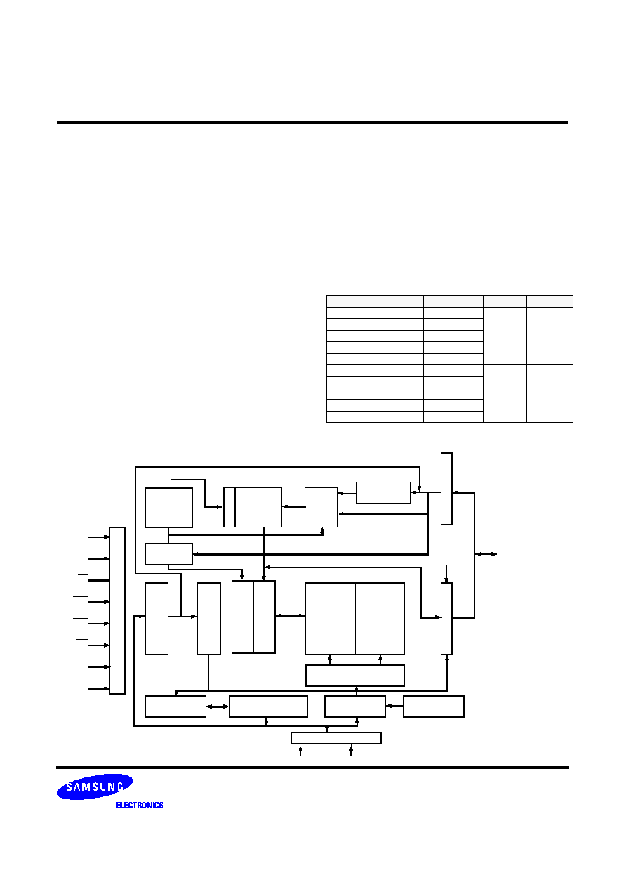
The K4G323222A is 33,554,432 bits synchronous high data
rate Dynamic RAM organized as 2 x 524,288 words by 32 bits,
fabricated with SAMSUNG
s high performance CMOS technol-
ogy. Synchronous design allows precise cycle control with the
use of system clock. I/O transactions are possible on every
clock cycle. Range of operating frequencies, programmable
burst length, and programmable latencies allows the same
device to be useful for a variety of high bandwidth, high perfor-
mance memory system applications.
8 columns block write improves performance in graphics sys-
tems.
· 3.3V power supply
· LVTTL compatible with multiplexed address
· Dual bank operation
· MRS cycle with address key programs
-. CAS Latency (2, 3)
-. Burst Length (1, 2, 4, 8 & full page)
-. Burst Type (Sequential & Interleave)
· All inputs are sampled at the positive going edge of the
system clock
· Burst Read Single-bit Write operation
· DQM 0-3 for byte masking
· Auto & self refresh
·
32ms refresh period (2K cycle)
· 100 Pin PQFP, TQFP (14 x 20 mm)
Graphics Features
· SMRS cycle.
-. Load color register
· Block Write(8 Columns)
GENERAL DESCRIPTION
FEATURES
FUNCTIONAL BLOCK DIAGRAM
512K x 32Bit x 2 Banks Synchronous Graphic RAM
T
I
M
I
N
G
R
E
G
I
S
T
E
R
CLK
CKE
CS
RAS
CAS
WE
DSF
DQMi
BLOCK
WRITE
CONTROL
LOGIC
DQi
P
R
O
G
R
A
M
I
N
G
R
E
G
I
S
T
E
R
L
A
T
E
N
C
Y
&
B
U
R
S
T
L
E
N
G
T
H
512Kx32
CELL
ARRAY
512Kx32
CELL
ARRAY
SERIAL
COUNTER
COLUMN ADDRESS
BUFFER
ROW DECORDER
BANK SELECTION
ADDRESS REGISTER
REFRESH
COUNTER
ROW ADDRESS
BUFFER
I
N
P
U
T
B
U
F
F
E
R
MUX
WRITE
CONTROL
LOGIC
M
A
S
K
C
O
L
U
M
N
D
E
C
O
R
D
E
R
S
E
N
S
E
A
M
P
L
I
F
I
E
R
COLUMN
MASK
(i=0~31)
DQMi
CLOCK ADDRESS(A
0
~A
10
,BA)
DQMi
O
U
T
P
U
T
B
U
F
F
E
R
·
·
ORDERING INFORMATION
Part NO.
Max Freq.
Interface
Package
K4G323222A-PC/L45
222MHz
LVTTL
100 PQFP
K4G323222A-PC/L50
200MHz
K4G323222A-PC/L7C
133MHz@CL2
K4G323222A-PC/L60
166MHz
K4G323222A-PC/L70
143MHz
K4G323222A-QC/L45
222MHz
LVTTL
100 TQFP
K4G323222A-QC/L50
200MHz
K4G323222A-QC/L7C
133MHz@CL2
K4G323222A-QC/L60
166MHz
K4G323222A-QC/L70
143MHz
Samsung Electronics reserves the right to
change products or specification without
notice.
*
COLOR
REGISTER
·
K4G323222A
CMOS SGRAM
- 4 -
Rev. 1.3 (Dec. 2000)
DQ29
V
SSQ
DQ30
DQ31
V
SS
N.C
N.C
N.C
N.C
N.C
N.C
N.C
N.C
N.C
N.C
V
DD
DQ0
DQ1
V
SSQ
DQ2
81
82
83
84
85
86
87
88
89
90
91
92
93
94
95
96
97
98
99
100
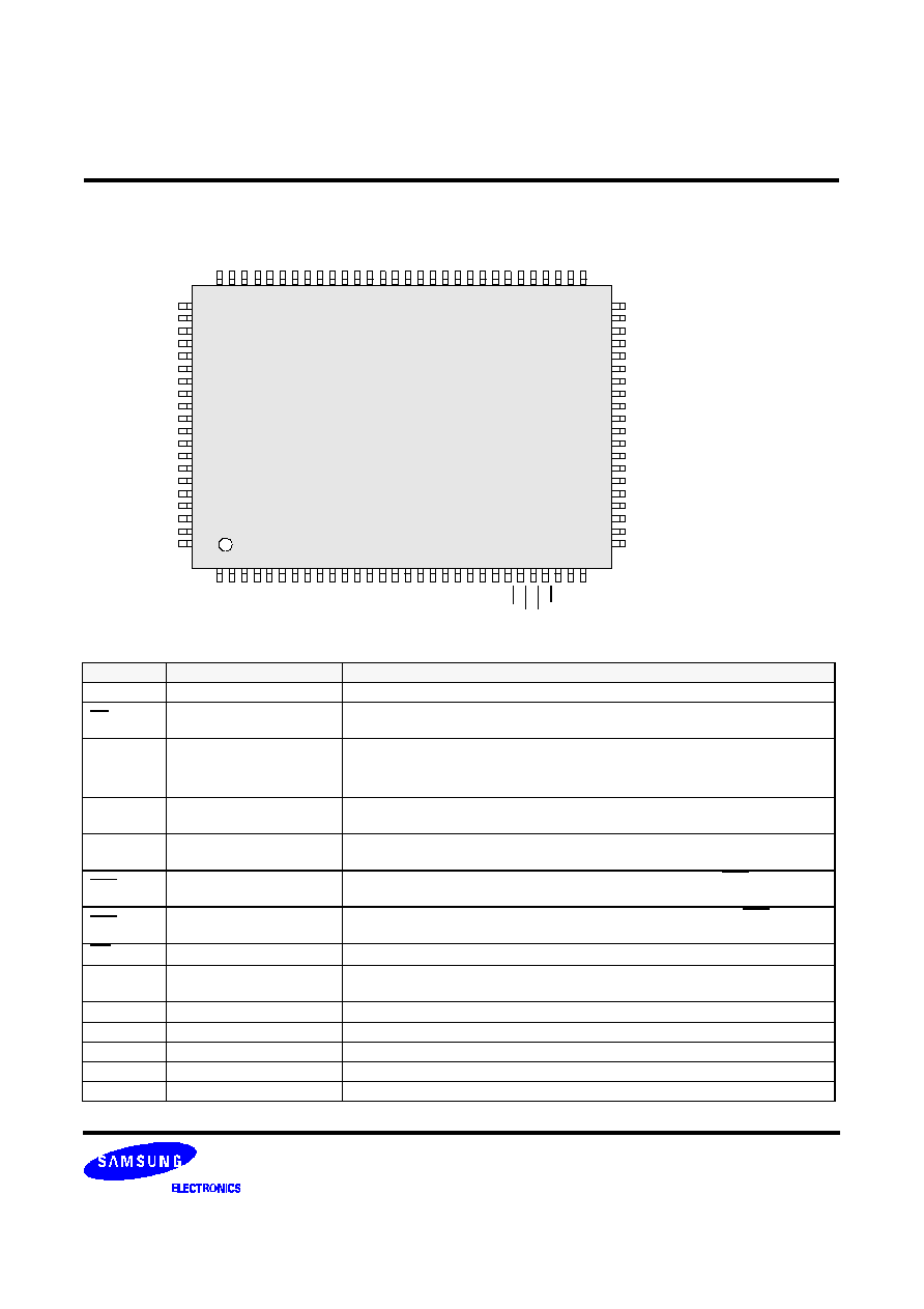
PIN CONFIGURATION (TOP VIEW)
D
Q
3
V
D
D
Q
D
Q
4
D
Q
5
V
S
S
Q
D
Q
6
D
Q
7
V
D
D
Q
D
Q
1
6
D
Q
1
7
V
S
S
Q
D
Q
1
8
D
Q
1
9
V
D
D
Q
V
D
D
V
S
S
D
Q
2
0
D
Q
2
1
V
S
S
Q
D
Q
2
2
D
Q
2
3
V
D
D
Q
D
Q
M
0
D
Q
M
2
W
E
C
A
S
R
A
S
C
S
B
A
A
9
1
2
3
4
5
6
7
8
9
1
0
1
1
1
2
1
3
1
4
1
5
1
6
1
7
1
8
1
9
2
0
2
1
2
2
2
3
2
4
2
5
2
6
2
7
2
8
2
9
3
0
A
7
A
6
A
5
A
4
V
SS
A
10
N.C
N.C
N.C
N.C
N.C
N.C
N.C
N.C
N.C
V
DD
A
3
A
2
A
1
A
0
50
49
48
47
46
45
44
43
42
41
40
39
38
37
36
35
34
33
32
31
100 Pin QFP
Forward Type
20 x 14 mm
2
0.65mm pin Pitch
D
Q
2
8
V
D
D
Q
D
Q
2
7
D
Q
2
6
V
S
S
Q
D
Q
2
5
D
Q
2
4
V
D
D
Q
D
Q
1
5
D
Q
1
4
V
S
S
Q
D
Q
1
3
D
Q
1
2
V
D
D
Q
V
S
S
V
D
D
D
Q
1
1
D
Q
1
0
V
S
S
Q
D
Q
9
D
Q
8
V
D
D
Q
N
.
C
D
Q
M
3
D
Q
M
1
C
L
K
C
K
E
D
S
F
N
.
C
A
8
/
A
P
8
0
7
9
7
8
7
7
7
6
7
5
7
4
7
3
7
2
7
1
7
0
6
9
6
8
6
7
6
6
6
5
6
4
6
3
6
2
6
1
6
0
5
9
5
8
5
7
5
6
5
5
5
4
5
3
5
2
5
1
PIN CONFIGURATION DESCRIPTION
PIN
NAME
INPUT FUNCTION
CLK
System Clock
Active on the positive going edge to sample all inputs.
CS
Chip Select
Disables or enables device operation by masking or enabling all inputs except
CLK, CKE and DQMi
CKE
Clock Enable
Masks system clock to freeze operation from the next clock cycle.
CKE should be enabled at least one clock + t
SS
prior to new command.
Disable input buffers for power down in standby.
A0 ~ A10
Address
Row / Column addresses are multiplexed on the same pins.
Row address : RA
0
~ RA
10
, Column address : CA
0
~ CA
7
BA
Bank Select Address
Selects bank to be activated during row address latch time.
Selects bank for read/write during column address latch time.
RAS
Row Address Strobe
Latches row addresses on the positive going edge of the CLK with RAS low.
Enables row access & precharge.
CAS
Column Address Strobe
Latches column addresses on the positive going edge of the CLK with CAS low.
Enables column access.
WE
Write Enable
Enables write operation and Row precharge.
DQMi
Data Input/Output Mask
Makes data output Hi-Z, t
SHZ
after the clock and masks the output.
Blocks data input when DQM active.(Byte Masking)
DQi
Data Input/Output
Data inputs/outputs are multiplexed on the same pins.
DSF
Define Special Function
block write and special mode register set.
V
DD
/V
SS
Power Supply /Ground
Power Supply : +3.3V
±
0.3V/Ground
V
DDQ
/V
SSQ
Data Output Power /Ground
Provide isolated Power/Ground to DQs for improved noise immunity.
N.C
No Connection
*PQFP (Height = 3.0mmMAX)
TQFP (Height = 1.2mmMAX)
K4G323222A
CMOS SGRAM
- 5 -
Rev. 1.3 (Dec. 2000)
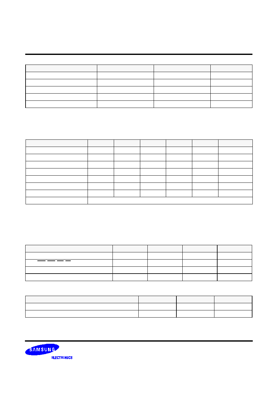
DECOUPLING CAPACITANCE GUIDE LINE
Recommended decoupling capacitance added to power line at board.
Parameter
Symbol
Value
Unit
Decoupling Capacitance between V
DD
and V
SS
C
DC1
0.1 + 0.01
uF
Decoupling Capacitance between V
DDQ
and V
SSQ
C
DC2
0.1 + 0.01
uF
1. V
DD
and V
DDQ
pins are separated each other.
All V
DD
pins are connected in chip. All V
DDQ
pins are connected in chip.
2. V
SS
and V
SSQ
pins are separated each other
All V
SS
pins are connected in chip. All V
SSQ
pins are connected in chip.
Note :
ABSOLUTE MAXIMUM RATINGS
(Voltage referenced to V
SS
)
Parameter
Symbol
Value
Unit
Voltage on any pin relative to Vss
V
IN
, V
OUT
-1.0
~
4.6
V
Voltage on V
DD
supply relative to Vss
V
DD
, V
DDQ
-1.0
~
4.6
V
Storage temperature
T
STG
-55 ~ +150
°
C
Power dissipation
P
D
1
W
Short circuit current
I
OS
50
mA
Permanent device damage may occur if "ABSOLUTE MAXIMUM RATINGS" are exceeded.
Functional operation should be restricted to recommended operating condition.
Exposure to higher than recommended voltage for extended periods of time could affect device reliability.
Note :
DC OPERATING CONDITIONS
Recommended operating conditions (Voltage referenced to V
SS
= 0V)
Parameter
Symbol
Min
Typ
Max
Unit
Note
Supply voltage
V
DD
, V
DDQ
3.0
3.3
3.6
V
5
Input high voltage
V
IH
2.0
3.0
V
DDQ
+0.3
V
1
Input low voltage
V
IL
-0.3
0
0.8
V
2
Output high voltage
V
OH
2.4
-
-
V
I
OH
= -2mA
Output low voltage
V
OL
-
-
0.4
V
I
OL
= 2mA
Input leakage current
I
LI
-10
-
10
uA
3
Output leakage current
I
LO
-10
-
10
uA
4
Output Loading Condition
see figure 1
1. V
IH
(max) = 5.6V AC. The overshoot voltage duration is
3ns.
2. V
IL
(min) = -2.0V AC. The undershoot voltage duration is
3ns.
3. Any input 0V
V
IN
V
DDQ
.
Input leakage currents include HI-Z output leakage for all bi-directional buffers with Tri-State outputs.
4. Dout is disabled, 0V
V
OUT
V
DD.
5. The VDD condition of K4G323222A-45/50/7C/60 is 3.135V~3.6V.
Note :
CAPACITANCE
(V
DD
/V
DDQ
= 3.3V, T
A
= 23
°
C, f = 1MHz)
Pin
Symbol
Min
Max
Unit
Clock
C
CLK
-
4.0
pF
RAS, CAS, WE, CS, CKE, DQM
i
,DSF
C
IN
-
4.0
pF
Address
C
ADD
-
4.0
pF
DQ
i
C
OUT
-
5.0
pF