
K4G323222M
CMOS SGRAM
Rev. 1.1 (Feb. 2000)
32Mbit SGRAM
Revision 1.1
February 2000
512K x 32bit x 2 Banks
Synchronous Graphic RAM
LVTTL
Samsung Electronics reserves the right to change products or specification without notice.

K4G323222M
CMOS SGRAM
Rev. 1.1 (Feb. 2000)
Revision History
Revision 1.1 (February,3 2000)
∑ Add K4G323222M-7C (133MHz@CL2,tRCD/tRP=2tCK).
Revision 1.0 (October 1999)
∑ Initial Release
K4G323222M
CMOS SGRAM
Rev. 1.1 (Feb. 2000)
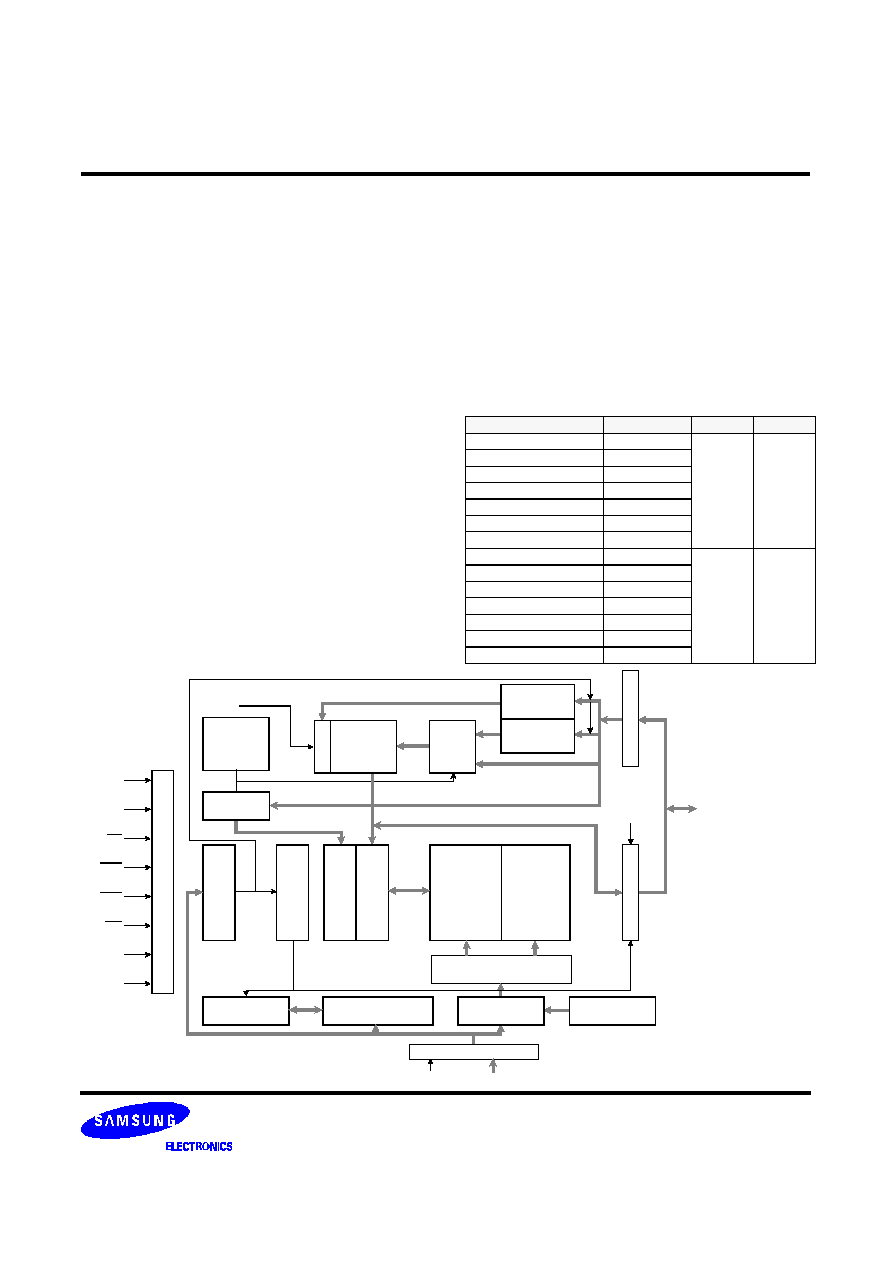
The K4G323222M is 33,554,432 bits synchronous high data
rate Dynamic RAM organized as 2 x 524,288 words by 32 bits,
fabricated with SAMSUNG
s high performance CMOS technol-
ogy. Synchronous design allows precise cycle control with the
use of system clock. I/O transactions are possible on every
clock cycle. Range of operating frequencies, programmable
burst length, and programmable latencies allows the same
device to be useful for a variety of high bandwidth, high perfor-
mance memory system applications.
Write per bit and 8 columns block write improves performance in
graphics systems.
∑ 3.3V power supply
∑ LVTTL compatible with multiplexed address
∑ Dual bank operation
∑ MRS cycle with address key programs
-. CAS Latency (2, 3)
-. Burst Length (1, 2, 4, 8 & full page)
-. Burst Type (Sequential & Interleave)
∑ All inputs are sampled at the positive going edge of the
system clock
∑ Burst Read Single-bit Write operation
∑ DQM 0-3 for byte masking
∑ Auto & self refresh
∑
32ms refresh period (2K cycle)
∑ 100 Pin PQFP, TQFP (14 x 20 mm)
Graphics Features
∑ SMRS cycle.
-. Load mask register
-. Load color register
∑ Write Per Bit(Old Mask)
∑ Block Write(8 Columns)
GENERAL DESCRIPTION
FEATURES
FUNCTIONAL BLOCK DIAGRAM
512K x 32Bit x 2 Banks Synchronous Graphic RAM
T
I
M
I
N
G
R
E
G
I
S
T
E
R
CLK
CKE
CS
RAS
CAS
WE
DSF
DQMi
BLOCK
WRITE
CONTROL
LOGIC
DQi
P
R
O
G
R
A
M
I
N
G
R
E
G
I
S
T
E
R
L
A
T
E
N
C
Y
&
B
U
R
S
T
L
E
N
G
T
H
512Kx32
CELL
ARRAY
512Kx32
CELL
ARRAY
SERIAL
COUNTER
COLUMN ADDRESS
BUFFER
ROW DECORDER
BANK SELECTION
ADDRESS REGISTER
REFRESH
COUNTER
ROW ADDRESS
BUFFER
I
N
P
U
T
B
U
F
F
E
R
MASK
REGISTER
COLOR
REGISTER
MUX
WRITE
CONTROL
LOGIC
M
A
S
K
C
O
L
U
M
N
D
E
C
O
R
D
E
R
S
E
N
S
E
A
M
P
L
I
F
I
E
R
COLUMN
MASK
(i=0~31)
DQMi
CLOCK ADDRESS(A
0
~A
10
,BA)
DQMi
O
U
T
P
U
T
B
U
F
F
E
R
∑
∑
∑
ORDERING INFORMATION
Part NO.
Max Freq.
Interface
Package
K4G323222M-PC/L45
222MHz
LVTTL
100 PQFP
K4G323222M-PC/L50
200MHz
K4G323222M-PC/L55
183MHz
K4G323222M-PC/L7C
133MHz@CL2
K4G323222M-PC/L60
166MHz
K4G323222M-PC/L70
143MHz
K4G323222M-PC/L80
125MHz
K4G323222M-QC/L45
222MHz
LVTTL
100 TQFP
K4G323222M-QC/L50
200MHz
K4G323222M-QC/L55
183MHz
K4G323222M-QC/L7C
133MHz@CL2
K4G323222M-QC/L60
166MHz
K4G323222M-QC/L70
143MHz
K4G323222M-QC/L80
125MHz
Samsung Electronics reserves the right to
change products or specification without
notice.
*
K4G323222M
CMOS SGRAM
Rev. 1.1 (Feb. 2000)
DQ29
V
SSQ
DQ30
DQ31
V
SS
N.C
N.C
N.C
N.C
N.C
N.C
N.C
N.C
N.C
N.C
V
DD
DQ0
DQ1
V
SSQ
DQ2
81
82
83
84
85
86
87
88
89
90
91
92
93
94
95
96
97
98
99
100
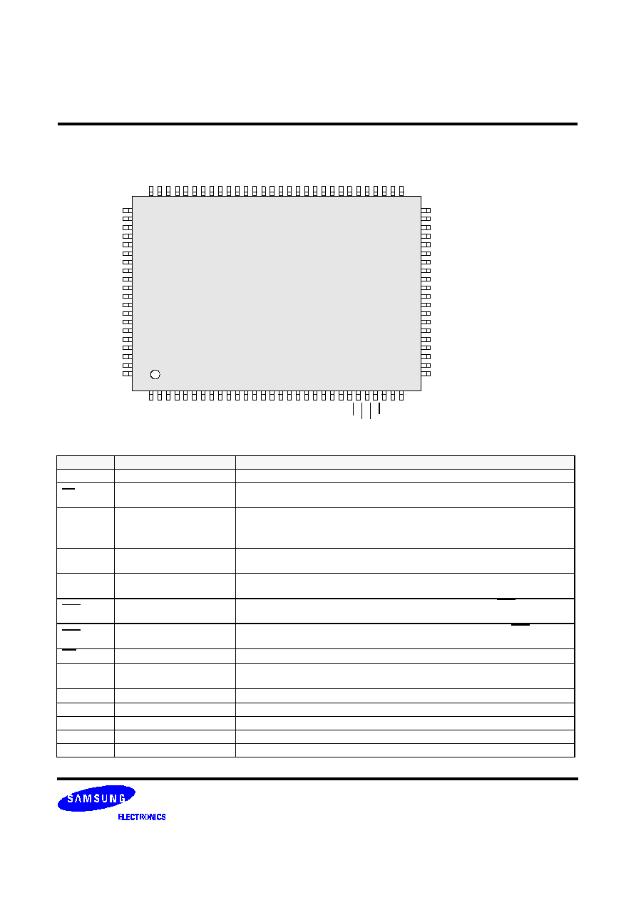
PIN CONFIGURATION (TOP VIEW)
D
Q
3
V
D
D
Q
D
Q
4
D
Q
5
V
S
S
Q
D
Q
6
D
Q
7
V
D
D
Q
D
Q
1
6
D
Q
1
7
V
S
S
Q
D
Q
1
8
D
Q
1
9
V
D
D
Q
V
D
D
V
S
S
D
Q
2
0
D
Q
2
1
V
S
S
Q
D
Q
2
2
D
Q
2
3
V
D
D
Q
D
Q
M
0
D
Q
M
2
W
E
C
A
S
R
A
S
C
S
B
A
A
9
1
2
3
4
5
6
7
8
9
1
0
1
1
1
2
1
3
1
4
1
5
1
6
1
7
1
8
1
9
2
0
2
1
2
2
2
3
2
4
2
5
2
6
2
7
2
8
2
9
3
0
A
7
A
6
A
5
A
4
V
SS
A
10
N.C
N.C
N.C
N.C
N.C
N.C
N.C
N.C
N.C
V
DD
A
3
A
2
A
1
A
0
50
49
48
47
46
45
44
43
42
41
40
39
38
37
36
35
34
33
32
31
100 Pin QFP
Forward Type
20 x 14 mm
2
0.65mm pin Pitch
D
Q
2
8
V
D
D
Q
D
Q
2
7
D
Q
2
6
V
S
S
Q
D
Q
2
5
D
Q
2
4
V
D
D
Q
D
Q
1
5
D
Q
1
4
V
S
S
Q
D
Q
1
3
D
Q
1
2
V
D
D
Q
V
S
S
V
D
D
D
Q
1
1
D
Q
1
0
V
S
S
Q
D
Q
9
D
Q
8
V
D
D
Q
N
.
C
D
Q
M
3
D
Q
M
1
C
L
K
C
K
E
D
S
F
N
.
C
A
8
/
A
P
8
0
7
9
7
8
7
7
7
6
7
5
7
4
7
3
7
2
7
1
7
0
6
9
6
8
6
7
6
6
6
5
6
4
6
3
6
2
6
1
6
0
5
9
5
8
5
7
5
6
5
5
5
4
5
3
5
2
5
1
PIN CONFIGURATION DESCRIPTION
PIN
NAME
INPUT FUNCTION
CLK
System Clock
Active on the positive going edge to sample all inputs.
CS
Chip Select
Disables or enables device operation by masking or enabling all inputs except
CLK, CKE and DQMi
CKE
Clock Enable
Masks system clock to freeze operation from the next clock cycle.
CKE should be enabled at least one clock + t
SS
prior to new command.
Disable input buffers for power down in standby.
A0 ~ A10
Address
Row / Column addresses are multiplexed on the same pins.
Row address : RA
0
~ RA
10
, Column address : CA
0
~ CA
7
BA
Bank Select Address
Selects bank to be activated during row address latch time.
Selects bank for read/write during column address latch time.
RAS
Row Address Strobe
Latches row addresses on the positive going edge of the CLK with RAS low.
Enables row access & precharge.
CAS
Column Address Strobe
Latches column addresses on the positive going edge of the CLK with CAS low.
Enables column access.
WE
Write Enable
Enables write operation and Row precharge.
DQMi
Data Input/Output Mask
Makes data output Hi-Z, t
SHZ
after the clock and masks the output.
Blocks data input when DQM active.(Byte Masking)
DQi
Data Input/Output
Data inputs/outputs are multiplexed on the same pins.
DSF
Define Special Function
Enables write per bit, block write and special mode register set.
V
DD
/V
SS
Power Supply /Ground
Power Supply : +3.3V
±
0.3V/Ground
V
DDQ
/V
SSQ
Data Output Power /Ground
Provide isolated Power/Ground to DQs for improved noise immunity.
N.C
No Connection
*PQFP (Height = 3.0mmMAX)
TQFP (Height = 1.2mmMAX)
K4G323222M
CMOS SGRAM
Rev. 1.1 (Feb. 2000)
DECOUPLING CAPACITANCE GUIDE LINE
Recommended decoupling capacitance added to power line at board.
Parameter
Symbol
Value
Unit
Decoupling Capacitance between V
DD
and V
SS
C
DC1
0.1 + 0.01
uF
Decoupling Capacitance between V
DDQ
and V
SSQ
C
DC2
0.1 + 0.01
uF
1. V
DD
and V
DDQ
pins are separated each other.
All V
DD
pins are connected in chip. All V
DDQ
pins are connected in chip.
2. V
SS
and V
SSQ
pins are separated each other
All V
SS
pins are connected in chip. All V
SSQ
pins are connected in chip.
Note :
ABSOLUTE MAXIMUM RATINGS
(Voltage referenced to V
SS
)
Parameter
Symbol
Value
Unit
Voltage on any pin relative to Vss
V
IN
, V
OUT
-1.0
~
4.6
V
Voltage on V
DD
supply relative to Vss
V
DD
, V
DDQ
-1.0
~
4.6
V
Storage temperature
T
STG
-55 ~ +150
∞
C
Power dissipation
P
D
1
W
Short circuit current
I
OS
50
mA
Permanent device damage may occur if "ABSOLUTE MAXIMUM RATINGS" are exceeded.
Functional operation should be restricted to recommended operating condition.
Exposure to higher than recommended voltage for extended periods of time could affect device reliability.
Note :
DC OPERATING CONDITIONS
Recommended operating conditions (Voltage referenced to V
SS
= 0V)
Parameter
Symbol
Min
Typ
Max
Unit
Note
Supply voltage
V
DD
, V
DDQ
3.0
3.3
3.6
V
5
Input high voltage
V
IH
2.0
3.0
V
DDQ
+0.3
V
1
Input low voltage
V
IL
-0.3
0
0.8
V
2
Output high voltage
V
OH
2.4
-
-
V
I
OH
= -2mA
Output low voltage
V
OL
-
-
0.4
V
I
OL
= 2mA
Input leakage current
I
LI
-10
-
10
uA
3
Output leakage current
I
LO
-10
-
10
uA
4
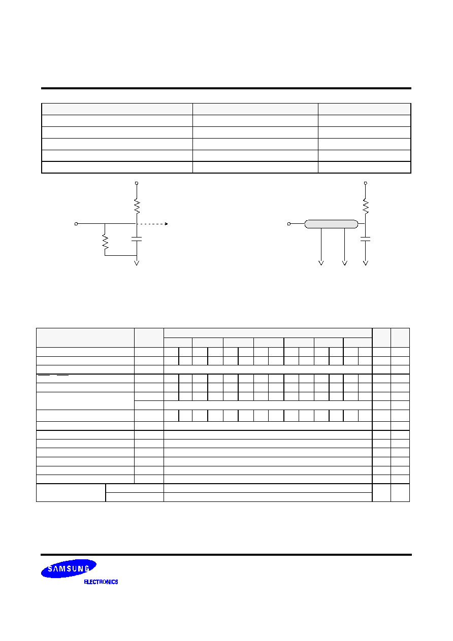
Output Loading Condition
see figure 1
1. V
IH
(max) = 5.6V AC. The overshoot voltage duration is
3ns.
2. V
IL
(min) = -2.0V AC. The undershoot voltage duration is
3ns.
3. Any input 0V
V
IN
V
DDQ
.
Input leakage currents include HI-Z output leakage for all bi-directional buffers with Tri-State outputs.
4. Dout is disabled, 0V
V
OUT
V
DD.
5. The VDD condition of K4G323222M-45/50/55/7C/60 is 3.135V~3.6V.
Note :
CAPACITANCE
(V
DD
/V
DDQ
= 3.3V, T
A
= 23
∞
C, f = 1MHz)
Pin
Symbol
Min
Max
Unit
Clock
C
CLK
-
4.0
pF
RAS, CAS, WE, CS, CKE, DQM
i
,DSF
C
IN
-
4.0
pF
Address
C
ADD
-
4.0
pF
DQ
i
C
OUT
-
5.0
pF
K4G323222M
CMOS SGRAM
Rev. 1.1 (Feb. 2000)
DC CHARACTERISTICS
(Recommended operating condition unless otherwise noted, T
A
= 0 to 70
∞
C, V
IH(min)
/V
IL(max)
=2.0V/0.8V)
Parameter
Symbol
Test Condition
CAS
Latency
Speed
Unit Note
-45 -50
-55
-7C
-60
-70
-80
Operating Current
(One Bank Active)
I
CC1
Burst Length =1
t
RC
t
RC
(min), t
CC
t
CC
(min), I
o
= 0mA
3
220 200
190
-
180 160 150
mA
2
2
-
150
150
200
150 150 150
Precharge Standby Current
in power-down mode
I
CC2
P
CKE
V
IL
(max), t
CC
= 15ns
2
mA
I
CC2
PS
CKE
&
CLK
V
IL
(max), t
CC
=
2
Precharge Standby Current
in non power-down mode
I
CC2
N
CKE
V
IH
(min), CS
V
IH
(min), t
CC
= 15ns
Input signals are changed one time during 30ns
30
mA
I
CC2
NS
CKE
V
IH
(min), CLK
V
IL
(max), t
CC
=
Input signals are stable
15
Active Standby Current
in power-down mode
I
CC3
P
CKE
V
IL
(max), t
CC
= 15ns
3
mA
I
CC3
PS
CKE
V
IL
(max), t
CC
=
3
Active Standby Current
in non power-down mode
(One Bank Active)
I
CC3
N
CKE
V
IH
(min), CS
V
IH
(min), t
CC
= 15ns
Input signals are changed one time during 30ns
50
mA
I
CC3
NS
CKE
V
IH
(min), CLK
V
IL
(max), t
CC
=
Input signals are stable
30
Operating Current
(Burst Mode)
I
CC4
I
o
= 0 mA, Page Burst
All bank Activated, t
CCD
= t
CCD
(min)
3
310 290
270
-
260 230 200
mA
2
2
-
160
160
290
160 160 160
Refresh Current
I
CC5
t
RC
t
RC
(min)
3
220 200
190
-
180 160 150
mA
3
2
-
150
150
200
150 150 150
Self Refresh Current
I
CC6
CKE
0.2V
2
mA
4
450
uA
5
Operating Current
(One Bank Block Write)
I
CC7
t
CC
t
CC
(min), I
o
=0mA, t
BWC
(min)
250 230
210
230
200 170 150 mA
1. Unless otherwise notes, Input level is CMOS(V
IH
/V
IL
=V
DDQ
/V
SSQ
) in LVTTL.
2. Measured with outputs open. Addresses are changed only one time during tcc(min).
3. Refresh period is 32ms. Addresses are changed only one time during tcc(min).
4. K4G323222M-C*
5. K4G323222M-L* : Low Power version
Note :
K4G323222M
CMOS SGRAM
Rev. 1.1 (Feb. 2000)
AC OPERATING TEST CONDITIONS
(V
DD
= 3.3V
±
0.3V, T
A
= 0 to 70
∞
C)
Parameter
Value
Unit
Input levels (V
ih
/V
il
)
2.4 / 0.4
V
Input timing measurement reference level
1.4
V
Input rise and fall time
t
r
/
t
f
=1 / 1
ns
Output timing measurement reference level
1.4
V
Output load condition
See Fig. 2
3.3V
1200
870
Output
30pF
V
OH
(DC) = 2.4V, I
OH
= -2mA
V
OL
(DC) = 0.4V, I
OL
= 2mA
V
tt
= 1.4V
50
Output
30pF
Z0=50
(Fig. 2) AC Output Load Circuit
(Fig. 1) DC Output Load Circuit
∑
∑
∑
∑
∑
OPERATING AC PARAMETER
1. The minimum number of clock cycles is determined by dividing the minimum time required with clock cycle time and then
rounding off to the next higher integer. Refer to the following ns-unit based AC table.
Note :
1. The VDD condition of K4G323222M-45/50/55/7C/60 is 3.135V~3.6V.
Note :
(AC operating conditions unless otherwise noted)
Parameter
Symbol
Version
Unit
Note
-45
-50
-55
-7C
-60
-70
-80
CAS Latency
CL
3
-
3
2
3
2
-
2
3
2
3
2
3
2
CLK
CLK cycle time
t
CC(min)
4.5
-
5
10
5.5
10
-
7.5
6
10
7
10
8
10
ns
Row active to row active delay
t
RRD(min)
2
CLK
1
RAS to CAS delay
t
RCD(min)
4
-
4
2
3
2
-
2
3
2
3
2
3
2
CLK
1
Row precharge time
t
RP(min)
4
-
4
2
3
2
-
2
3
2
3
2
3
2
CLK
1
Row active time
t
RAS(min)
9
-
8
5
7
5
-
6
7
5
7
5
6
5
CLK
1
t
RAS(max)
100
us
Row cycle time
t
RC
(
min
)
13
-
12
7
10
7
-
8
10
7
10
7
9
7
CLK
1
Last data in to row precharge
t
RDL(min)
2
CLK
2, 5
Last data in to new col.address delay
t
CDL(min)
1
CLK
2
Last data in to burst stop
t
BDL(min)
1
CLK
2
Col. address to col. address delay
t
CCD(min)
1
CLK
Block Write data-in to PRE command
t
BPL(min)
2
CLK
Block write cycle time
t
BWC(min)
1
CLK
3
Mode Register Set cycle time
t
MRS(min)
1
CLK
Number of valid output
data
CAS Latency=3
2
ea
4
CAS Latency=2
1
K4G323222M
CMOS SGRAM
Rev. 1.1 (Feb. 2000)
1. Parameters depend on programmed CAS latency.
2. If clock rising time is longer than 1ns, (tr/2-0.5)ns should be added to the parameter.
3. Assumed input rise and fall time (tr & tf)=1ns.
If tr & tf is longer than 1ns, transient time compensation should be considered,
i.e., [(tr + tf)/2-1]ns should be added to the parameter.
Note :
AC CHARACTERISTICS
(AC operating conditions unless otherwise noted)
Parameter
Symbol
-45
-50
-55
-7C
-60
-70
-80
Unit Note
Min Max Min Max Min Max
Min Max
Min
Max Min Max Min Max
CLK cycle
time
CAS Latency=3
t
CC
4.5
1000
5
1000
5.5
1000
-
1000
6
1000
7
1000
8
1000
ns
1
CAS Latency=2
-
10
10
7.5
10
10
10
CLK to valid
output delay
CAS Latency=3
t
SAC
-
4
-
4.5
-
5
-
-
-
5.5
-
5.5
-
6
ns
1, 2
CAS Latency=2
-
-
-
6
-
6
-
6
-
6
-
6
-
6
Output data hold time
t
OH
2
-
2
-
2
-
2
-
2.5
-
2.5
-
2.5
-
ns
2
CLK high
pulse width
CAS Latency=3
t
CH
1.75
-
2
-
2
-
-
2.5
-
3
-
3
-
ns
3
CAS Latency=2
-
-
3
-
3
-
2
3
3
3
CLK low
pulse width
CAS Latency=3
t
CL
1.75
-
2
-
2
-
-
2.5
-
3
-
3
-
ns
3
CAS Latency=2
-
-
3
-
3
-
2
3
3
3
Input setup
time
CAS Latency=3
t
SS
1.2
-
1.5
-
1.5
-
-
-
1.5
-
1.75
-
2
-
ns
3
CAS Latency=2
-
-
2.5
-
2.5
-
1.5
2.5
2.5
2.5
Input hold time
t
SH
0.7
-
1
-
1
-
1
-
1
-
1
-
1
-
ns
3
CLK to output in Low-Z
t
SLZ
1
-
1
-
1
-
1
-
1
-
1
-
1
-
ns
2
CLK to out-
put
in Hi-Z
CAS latency=3
t
SHZ
-
4
-
4.5
-
5
-
-
-
5.5
-
5.5
-
6
ns
-
CAS latency=2
-
-
-
-
-
-
-
6.0
-
-
-
-
-
6
Parameter
Symbol
Version
Unit
-45
-50
-55
-7C
-60
-70
-80
CLK cycle time
t
CC(min)
4.5
5
5.5
7.5
6
7
8
ns
Row active to row active delay t
RRD(min)
9
10
11
15
12
14
16
ns
RAS to CAS delay
t
RCD(min)
18
20
16.5
15
18
21
20
ns
Row precharge time
t
RP(min)
18
20
16.5
15
18
21
20
ns
Row active time
t
RAS(min)
40.5
40
38.5
45
42
49
48
ns
t
RAS(max)
100
us
Row cycle time
t
RC
(
min
)
58.5
60
55
60
60
70
70
ns
2. Minimum delay is required to complete write.
3. This parameter means minimum CAS to CAS delay at block write cycle only.
4. In case of row precharge interrupt, auto precharge and read burst stop.
5. For -55/60/70/80, tRDL =1CLK product can be supported within restricted amounts and it will be distinguished by bucket code
"NV".
From the next generation, tRDL will be only 2CLK for every clock frequency.
K4G323222M
CMOS SGRAM
Rev. 1.1 (Feb. 2000)
SIMPLIFIED TRUTH TABLE
(V=Valid, X=Don
t Care, H=Logic High, L=Logic Low)
COMMAND
CKEn-1 CKEn
CS
RAS CAS WE DSF DQM BA A
8
A
10
,A
9
,A
7
~A
0
Note
Register
Mode Register Set
H
X
L
L
L
L
L
X
OP CODE
1, 2
Special Mode Register Set
H
1,2,7
Refresh
Auto Refresh
H
H
L
L
L
H
L
X
X
3
Self
Refresh
Entry
L
3
Exit
L
H
L
H
H
H
X
X
X
3
H
X
X
X
3
Bank Active
& Row Addr.
Write Per Bit Disable
H
X
L
L
H
H
L
X
V
Row Address
4, 5
Write Per Bit Enable
H
4,5,9
Read &
Column
Address
Auto Precharge Disable
H
X
L
H
L
H
L
X
V
L
Column
Address
(A
0
~A
7
)
4
Auto Precharge Enable
H
4, 6
Write &
Column
Address
Auto Precharge Disable
H
X
L
H
L
L
L
X
V
L
Column
Address
(A
0
~A
7
)
4, 5
Auto Precharge Enable
H
4,5,6,9
Block Write
&
Column
Auto Precharge Disable
H
X
L
H
L
L
H
X
V
L
Column
Address
(A
0
~A
7
)
4, 5
Auto Precharge Enable
H
4,5,6,9
Burst Stop
H
X
L
H
H
L
L
X
X
7
Precharge
Bank Selection
H
X
L
L
H
L
L
X
V
L
X
Both Banks
X
H
Clock Suspend or
Active Power Down
Entry
H
L
L
H
H
H
X
X
X
H
X
X
X
Exit
L
H
X
X
X
X
X
X
Precharge Power Down
Mode
Entry
H
L
L
H
H
H
X
X
X
H
X
X
X
Exit
L
H
L
V
V
V
V
X
H
X
X
X
X
DQM
H
X
V
X
8
No Operation Command
H
X
L
H
H
H
X
X
X
H
X
X
X
1. OP Code : Operand Code
A
0
~ A
10
, BA : Program keys. (@MRS)
A
5
, A
6
: LMR or LCR select. (@SMRS)
Color register exists only one per DQi which both banks share.
So dose Mask Register.
Color or mask is loaded into chip through DQ pin.
2. MRS can be issued only at both banks precharge state.
SMRS can be issued only if DQ
s are idle.
A new command can be issued at the next clock of MRS/SMRS.
Note :
K4G323222M
CMOS SGRAM
Rev. 1.1 (Feb. 2000)
SGRAM vs SDRAM
If DSF is low, SGRAM functionality is identical to SDRAM functionality.
SGRAM can be used as an unified memory by the appropriate DSF control
--> SGRAM=Graphic Memory + Main Memory
Function
MRS
Bank Active
Write
DSF
L
H
L
H
L
H
SGRAM
Function
MRS
SMRS
Bank Active
with
Write per bit
Disable
Bank Active
with
Write per bit
Enable
Normal
Write
Block
Write
3. Auto refresh functions as same as CBR refresh of DRAM.
The automatical precharge without Row precharge command is meant by "Auto".
Auto/Self refresh can be issued only at both precharge state.
4. BA : Bank select address.
If "Low" at read, (block) write, Row active and precharge, bank A is selected.
If "High" at read, (block) write, Row active and precharge, bank B is selected.
If A
8
is "High" at Row precharge, BA is ignored and both banks are selected.
5. It is determined at Row active cycle.
whether Normal/Block write operates in write per bit mode or not.
For A bank write, at A bank Row active, for B bank write, at B bank Row active.
Terminology : Write per bit =I/O mask
(Block) Write with write per bit mode=Masked(Block) Write
6. During burst read or write with auto precharge, new read/(block) write command cannot be issued.
Another bank read/(block) write command can be issued at
t
RP
after the end of burst.
7. Burst stop command is valid only at full page burst length.
8. DQM sampled at positive going edge of a CLK.
masks the data-in at the very CLK(Write DQM latency is 0)
but makes Hi-Z state the data-out of 2 CLK cycles after.(Read DQM latency is 2)
9. Graphic features added to SDRAM
s original features.
If DSF is tied to low, graphic functions are disabled and chip operates as a 32M SDRAM with 32 DQ
s.
SIMPLIFIED TRUTH TABLE
K4G323222M
CMOS SGRAM
Rev. 1.1 (Feb. 2000)
(Note 4)
Load Color
Load Mask
A
6
Function
A
5
Function
0
Disable
0
Disable
1
Enable
1
Enable
SGRAMs must be powered up and initialized in a predefined manner to prevent undefined operations.
1. Apply power and start clock. Must maintain CKE= "H", DQM= "H" and the other pins are NOP condition at the inputs.
2. Maintain stable power, stable clock and NOP input condition for a minimum of 200us.
3. Issue precharge commands for all banks of the devices.
4. Issue 2 or more auto-refresh commands.
5. Issue a mode register set command to initialize the mode register.
cf.) Sequence of 4 & 5 may be changed.
The device is now ready for normal operation.
Note : 1. RFU(Reserved for Future Use) should stay "0" during MRS cycle.
2. If A
9
is high during MRS cycle, "Burst Read Single Bit Write" function will be enabled.
3. The full column burst(256bit) is available only at Sequential mode of burst type.
4. If LC and LM both high(1), data of mask and color register will be unknown.
Register Programmed with MRS
(Note 1) (Note 2)
Address
BA
A
10
A
9
A
8
A
7
A
6
A
5
A
4
A
3
A
2
A
1
A
0
Function
RFU
W.B.L
TM
CAS Latency
BT
Burst Length
(Note 3)
Test Mode
CAS Latency
Burst Type
Burst Length
A
8
A
7
Type
A
6
A
5
A
4
Latency
A
3
Type
A
2
A
1
A
0
BT=0
BT=1
0
0
Mode Register Set
0
0
0
Reserved
0
Sequential
0
0
0
1
Reserved
0
1
Vendor
Use
Only
0
0
1
-
1
Interleave
0
0
1
2
Reserved
1
0
0
1
0
2
0
1
0
4
4
1
1
0
1
1
3
0
1
1
8
8
Write Burst Length
1
0
0
Reserved
1
0
0
Reserved
Reserved
A
9
Length
1
0
1
Reserved
1
0
1
Reserved
Reserved
0
Burst
1
1
0
Reserved
1
1
0
Reserved
Reserved
1
Single Bit
1
1
1
Reserved
1
1
1
256(Full)
Reserved
Special Mode Register Programmed with SMRS
Address
BA
A
10
A
9
A
8
A
7
A
6
A
5
A
4
A
3
A
2
A
1
A
0
Function
X
LC
LM
X
MODE REGISTER FIELD TABLE TO PROGRAM MODES
POWER UP SEQUENCE
K4G323222M
CMOS SGRAM
Rev. 1.1 (Feb. 2000)
BURST SEQUENCE (BURST LENGTH = 4)
Initial address
Sequential
Interleave
A
1
A
0
0
0
0
1
2
3
0
1
2
3
0
1
1
2
3
0
1
0
3
2
1
0
2
3
0
1
2
3
0
1
1
1
3
0
1
2
3
2
1
0
BURST SEQUENCE (BURST LENGTH = 8)
Initial address
Sequential
Interleave
A
2
A
1
A
0
0
0
0
0
1
2
3
4
5
6
7
0
1
2
3
4
5
6
7
0
0
1
1
2
3
4
5
6
7
0
1
0
3
2
5
4
7
6
0
1
0
2
3
4
5
6
7
0
1
2
3
0
1
6
7
4
5
0
1
1
3
4
5
6
7
0
1
2
3
2
1
0
7
6
5
4
1
0
0
4
5
6
7
0
1
2
3
4
5
6
7
0
1
2
3
1
0
1
5
6
7
0
1
2
3
4
5
4
7
6
1
0
3
2
1
1
0
6
7
0
1
2
3
4
5
6
7
4
5
2
3
0
1
1
1
1
7
0
1
2
3
4
5
6
7
6
5
4
3
2
1
0
PIXEL to DQ MAPPING(at BLOCK WRITE)
Column address
3 Byte
2 Byte
1 Byte
0 Byte
A
2
A
1
A
0
I/O
31
- I/O
24
I/O
23
- I/O
16
I/O
15
- I/O
8
I/O
7
- I/O
0
0
0
0
DQ
24
DQ
16
DQ
8
DQ
0
0
0
1
DQ
25
DQ
17
DQ
9
DQ
1
0
1
0
DQ
26
DQ
18
DQ
10
DQ
2
0
1
1
DQ
27
DQ
19
DQ
11
DQ
3
1
0
0
DQ
28
DQ
20
DQ
12
DQ
4
1
0
1
DQ
29
DQ
21
DQ
13
DQ
5
1
1
0
DQ
30
DQ
22
DQ
14
DQ
6
1
1
1
DQ
31
DQ
23
DQ
15
DQ
7

K4G323222M
CMOS SGRAM
Rev. 1.1 (Feb. 2000)
CLOCK (CLK)
The clock input is used as the reference for all SGRAM opera-
tions. All operations are synchronized to the positive going edge
of the clock. The clock transitions must be monotonic between
V
IL
and V
IH
. During operation with CKE high all inputs are
assumed to be in a valid state (low or high) for the duration of
set-up and hold time around positive edge of the clock for proper
functionality and I
CC
specifications.
CLOCK ENABLE (CKE)
The clock enable(CKE) gates the clock onto SGRAM. If CKE
goes low synchronously with clock (set-up and hold time are the
same as other inputs), the internal clock is suspended from the
next clock cycle and the state of output and burst address is fro-
zen as long as the CKE remains low. All other inputs are ignored
from the next clock cycle after CKE goes low. When both banks
are in the idle state and CKE goes low synchronously with clock,
the SGRAM enters the power down mode from the next clock
cycle. The SGRAM remains in the power down mode ignoring
the other inputs as long as CKE remains low. The power down
exit is synchronous as the internal clock is suspended. When
CKE goes high at least "
t
SS
+ 1
CLOCK
" before the high going
edge of the clock, then the SGRAM becomes active from the
same clock edge accepting all the input commands.
BANK SELECT (BA)
This SGRAM is organized as two independent banks of 524,288
words x 32 bits memory arrays. The BA inputs is latched at the
time of assertion of RAS and CAS to select the bank to be used
for the operation. When BA is asserted low, bank A is selected.
When BA is asserted high, bank B is selected. The bank select
BA is latched at bank activate, read, write mode register set and
precharge operations.
ADDRESS INPUT (A
0
~ A
10
)
The 19 address bits required to decode the 524,288 word loca-
tions are multiplexed into 11 address input pins(A
0
~A
10
). The 11
bit row address is latched along with RAS and BA during bank
activate command. The 8 bit column address is latched along
with CAS, WE and BA during read or write command.
NOP and DEVICE DESELECT
When RAS, CAS and WE are high, the SGRAM performs no
operation (NOP). NOP does not initiate any new operation, but
is needed to complete operations which require more than sin-
gle clock cycle like bank activate, burst read, auto refresh, etc.
The device deselect is also a NOP and is entered by asserting
CS high. CS high disables the command decoder so that RAS,
CAS, WE, DSF and all the address inputs are ignored.
POWER-UP
SGRAMs must be powered up and initialized in a pre-
defined manner to prevent undefined operations.
1. Power must be applied to both CKE and DQM inputs to pull
them high and other pins are NOP condition at the inputs
before or along with V
DD
(and V
DDQ
) supply.
The clock signal must also be asserted at the same time.
2. After V
DD
reaches the desired voltage, a minimum pause of
200 microseconds is required with inputs in NOP condition.
3. Both banks must be precharged now.
4. Perform a minimum of 2 Auto refresh cycles to stabilize the
internal circuitry.
5. Perform a MODE REGISTER SET cycle to program the CAS
latency, burst length and burst type as the default value of
mode register is undefined.
At the end of one clock cycle from the mode register set cycle,
the device is ready for operation.
When the above sequence is used for Power-up, all the outputs
will be in high impedance state. The high impedance of outputs
is not guaranteed in any other power-up sequence.
cf.) Sequence of 4 & 5 may be changed.
MODE REGISTER SET (MRS)
The mode register stores the data for controlling the various
operating modes of SGRAM. It programs the CAS latency,
addressing mode, burst length, test mode and various vendor
specific options to make SGRAM useful for variety of different
applications. The default value of the mode register is not
defined, therefore the mode register must be written after power
up to operate the SGRAM. The mode register is written by
asserting low on CS, RAS, CAS, WE and DSF (The SGRAM
should be in active mode with CKE already high prior to writing
the mode register). The state of address pins A
0
~ A
10
and BA in
the same cycle as CS, RAS, CAS, WE and DSF going low is the
data written in the mode register. One clock cycle is required to
complete the write in the mode register. The mode register con-
tents can be changed using the same command and clock cycle
requirements during operation as long as both banks are in the
idle state. The mode register is divided into various fields
depending on functionality. The burst length field uses A
0
~ A
2
,
burst type uses A
3
, addressing mode uses A
4
~ A
6
, A
7
~ A
8
, A
10
and BA are used for vendor specific options or test mode. And
the write burst length is programmed using A
9
. A
7
~ A
8
, A
10
and
BA
must be set to low for normal SGRAM operation. Refer to
table for specific codes for various burst length, addressing
modes and CAS latencies.
DEVICE OPERATIONS

K4G323222M
CMOS SGRAM
Rev. 1.1 (Feb. 2000)
BANK ACTIVATE
The bank activate command is used to select a random row in
an idle bank. By asserting low on RAS and CS with desired row
and bank addresses, a row access is initiated. The read or write
operation can occur after a time delay of t
RCD
(min) from the time
of bank activation. t
RCD
(min) is an internal timing parameter of
SGRAM, therefore it is dependent on operating clock frequency.
The minimum number of clock cycles required between bank
activate and read or write command should be calculated by
dividing t
RCD
(min) with cycle time of the clock and then rounding
off the result to the next higher integer. The SGRAM has two
internal banks on the same chip and shares part of the internal
circuitry to reduce chip area, therefore it restricts the activation
of both banks immediately. Also the noise generated during
sensing of each bank of SGRAM is high requiring some time for
power supplies to recover before the other bank can be sensed
reliably. t
RRD
(min) specifies the minimum time required between
activating different banks. The number of clock cycles required
between different bank activation must be calculated similar to
t
RCD
specification. The minimum time required for the bank to be
active to initiate sensing and restoring the complete row of
dynamic cells is determined by t
RAS
(min) specification before a
precharge command to that active bank can be asserted. The
maximum time any bank can be in the active state is determined
by t
RAS
(max). The number of cycles for both t
RAS
(min) and
t
RAS
(max) can be calculated similar to t
RCD
specification.
BURST READ
The burst read command is used to access burst of data on con-
secutive clock cycles from an active row in an active bank. The
burst read command is issued by asserting low on CS and CAS
with WE being high on the positive edge of the clock. The bank
must be active for at least t
RCD
(min) before the burst read com-
mand is issued. The first output appears CAS latency number of
clock cycles after the issue of burst read command. The burst
length, burst sequence and latency from the burst read com-
mand is determined by the mode register which is already pro-
grammed. The burst read can be initiated on any column
address of the active row. The address wraps around if the initial
address does not start from a boundary such that number of out-
puts from each I/O are equal to the burst length programmed in
the mode register. The output goes into high-impedance at the
end of the burst, unless a new burst read was initiated to keep
the data output gapless. The burst read can be terminated by
issuing another burst read or burst write in the same bank or the
other active bank or a precharge command to the same bank.
The burst stop command is valid only at full page burst length
where the output does not go into high impedance at the end of
burst and the burst is wrapped around..
BURST WRITE
The burst write command is similar to burst read command, and
is used to write data into the SGRAM on consecutive clock
cycles in adjacent addresses depending on burst length and
burst sequence. By asserting low on CS, CAS and WE with valid
column address, a write burst is initiated. The data inputs are
provided for the initial address in the same clock cycle as the
burst write command. The input buffer is deselected at the end
of the burst length, even though the internal writing may not
have been completed yet. The writing can not complete to burst
length. The burst write can be terminated by issuing a burst
read and DQM for blocking data inputs or burst write in the same
or the other active bank. The burst stop command is valid only at
full page burst length where the writing continues at the end of
burst and the burst is wrapped around. The write burst can also
be terminated by using DQM for blocking data and precharging
the bank "t
RDL
" after the last data input to be written into the
active row. See DQM OPERATION also.
DQM OPERATION
The DQM is used to mask input and output operations. It works
similar to OE during read operation and inhibits writing during
write operation. The read latency is two cycles from DQM and
zero cycle for write, which means DQM masking occurs two
cycles later in the read cycle and occurs in the same cycle dur-
ing write cycle. DQM operation is synchronous with the clock,
therefore the masking occurs for a complete cycle. The DQM
signal is important during burst interrupts of write with read or
precharge in the SGRAM. Due to asynchronous nature of the
internal write, the DQM operation is critical to avoid unwanted or
incomplete writes when the complete burst write is not required.
DQM is also used for device selection, byte selection and bus
control in a memory system. DQM0 controls DQ0 to DQ7,
DQM1 controls DQ8 to DQ15, DQM2 controls DQ16 to DQ23,
DQM3 controls DQ24 to DQ31. DQM masks the DQ
s by a byte
regardless that the corresponding DQ
s are in a state of WPB
masking or Pixel masking. Please refer to DQM timing diagram
also.
PRECHARGE
The precharge operation is performed on an active bank by
asserting low on CS, RAS, WE and A
8
/AP
with valid BA of the
bank to be precharged. The precharge command can be
asserted anytime after t
RAS
(min) is satisfied from the bank acti-
vate command in the desired bank. "t
RP
" is defined as the mini-
mum time required to precharge a bank. The minimum number
of clock cycles required to complete row precharge is calculated
by dividing "t
RP
" with clock cycle time and rounding up to the
next higher integer. Care should be taken to make sure that
burst write is completed or DQM is used to inhibit writing before
precharge command is asserted. The maximum time any bank
can be active is specified by t
RAS
(max). Therefore, each bank
has to be precharged within t
RAS
(max)
from the bank
activate
command. At the end of precharge, the bank enters the idle
state and is ready to be activated again.
DEVICE OPERATIONS

K4G323222M
CMOS SGRAM
Rev. 1.1 (Feb. 2000)
Entry to Power Down, Auto refresh, Self refresh and Mode reg-
ister Set etc. is possible only when both banks are in idle state.
AUTO PRECHARGE
The precharge operation can also be performed by using auto
precharge. The SGRAM internally generates the timing to satisfy
t
RAS
(min) and "t
RP
" for the programmed burst length and CAS
latency. The auto precharge command is issued at the same
time as burst read or burst write by asserting high on A
8
/AP
. If
burst read or burst write command is issued with low on A
8
/AP
,
the bank is left active until a new command is asserted. Once
auto precharge command is given, no new commands are pos-
sible to that particular bank until the bank achieves idle state.
BOTH BANKS PRECHARGE
Both banks can be precharged at the same time by using Pre-
charge all command. Asserting low on CS, RAS, and WE with
high on A
8/AP
after both banks have satisfied t
RAS
(min) require-
ment, performs precharge on both banks. At the end of t
RP
after
performing precharge all, both banks are in idle state.
AUTO REFRESH
The storage cells of SGRAM need to be refreshed every 32ms
to maintain data. An auto refresh cycle accomplishes refresh of
a single row of storage cells. The internal counter increments
automatically on every auto refresh cycle to refresh all the rows.
An auto refresh command is issued by asserting low on CS,RAS
and CAS with high on CKE and WE. The auto refresh command
can only be asserted with both banks being in idle state and the
device is not in power down mode (CKE is high in the previous
cycle). The time required to complete the auto refresh operation
is specified by "t
RC
(min)". The minimum number of clock cycles
required can be calculated by driving "t
RC
" with clock cycle time
and them rounding up to the next higher integer. The auto
refresh command must be followed by NOP
s until the auto
refresh operation
i
s completed. Both banks will be in the idle
state at the end of auto refresh operation. The auto refresh is the
preferred refresh mode when the SGRAM is being used for nor-
mal data transactions. The auto refresh cycle can be performed
once in 15.6us or a burst of 2048 auto refresh cycles once in
32ms.
SELF REFRESH
The self refresh is another refresh mode available in the
SGRAM. The self refresh is the preferred refresh mode for data
retention and low power operation of SGRAM. In self refresh
mode, the SGRAM disables the internal clock and all the input
buffers except CKE. The refresh addressing and timing are
internally generated to reduce power consumption.
The self refresh mode is entered from all banks idle state by
asserting low on CS, RAS, CAS and CKE with high on WE.
Once the self refresh mode is entered, only CKE state being low
matters, all the other inputs including the clock are ignored in
order to remain in the self refresh mode.
The self refresh is exited by restarting the external clock and
then asserting high on CKE. This must be followed by NOP
s
for a minimum time of "t
RC
" before the SGRAM reaches idle
state to begin normal operation. If the system uses burst auto
refresh during normal operation, it is recommended to use burst
2048 auto refresh cycles immediately after exiting self refresh.
DEFINE SPECIAL FUNCTION(DSF)
The DSF controls the graphic applications of SGRAM. If DSF is
tied to low, SGRAM functions as 512K x 32 x2 Bank SDRAM.
SGRAM can be used as an unified memory by the appropriate
DSF command. All the graphic function modes can be entered
only by setting DSF high when issuing commands which other-
wise would be normal SDRAM commands. SDRAM functions
such as RAS Active, Write, and WCBR change to SGRAM func-
tions such as RAS Active with WPB, Block Write and SWCBR
respectively. See the section below for the graphic functions that
DSF controls.
SPECIAL MODE REGISTER SET(SMRS)
There are two kinds of special mode registers in SGRAM.One is
color register and the other is mask register. Those usage will be
explained in the "WRITE PER BIT" and "BLOCK WRITE" sec-
tions. When A
5
and DSF goes high in the same cycle as CS,
RAS, CAS and WE going low, Load Mask Register(LMR) pro-
cess is executed and the mask registers are filled with the
masks for associated DQ
s through DQ pins. And when A
6
and
DSF goes high in the same cycle as CS, RAS, CAS and WE
going low, Load Color Register(LCR) process is executed and
the color register is filled with color data for associated DQ
s
through the DQ pins. If both A
5
and A
6
are high at SMRS, data
of mask and color cycle are required to complete the write in the
mask register and the color register at LMR and LCR respec-
tively. A new command can be issued in the next clock of LMR
or LCR. SMRS, compared with MRS, can be issued at the active
state under the condition that DQ
s are idle. As in write opera-
tion, SMRS accepts the data needed through DQ pins. There-
fore bus contention must be avoided. The more detailed
materials can be obtained by referring corresponding timing dia-
gram.
DEVICE OPERATIONS (Continued)
K4G323222M
CMOS SGRAM
Rev. 1.1 (Feb. 2000)
WRITE PER BIT
Write per bit(i.e. I/O mask mode) for SGRAM is a function that
selectively masks bits of data being written to the devices. The
mask is stored in an internal register and applied to each bit of
data written when the mask is enabled. Bank active command
with DSF=High enables write per bit for associated bank. Bank
active command with DSF=Low disables write per bit for the
associated bank. The mask used for write per bit operations is
stored in the mask register accessed by SWCBR(Special Mode
Register Set Command). When a mask bit=1, the associated
data bit is written when a write command is executed and write
per bit has been enabled for the bank being written. When a
mask bit=0, the associated data bit is unaltered when a write
command is executed and the write per bit has been enabled for
the bank being written. No additional timing conditions are
required for write per bit operations. Write per bit writes can be
either single write, burst writes or block writes. DQM masking is
the same for write per bit and non-WPB write.
BLOCK WRITE
Block write is a feature allowing the simultaneous writing of
consecutive 8 columns of data within a RAM device during a sin-
gle access cycle. During block write the data to be written comes
from an internal "color" register and DQ I/O pins are used for
independent column selection. The block of column to be written
is aligned on 8 column boundaries and is defined by the column
address with the 3 LSB
s ignored. Write command with DSF=1
enables block write for the associated bank. A write command
with DSF=0 enables normal write for the associated bank. The
block width is 8 column where column="n" bits for by "n" part.
The color register is the same width as the data port of the
chip.It is written via a SWCBR where data present on the DQ pin
is to be coupled into the internal color register. The color register
provides the data masked by the DQ column select, WPB
mask(If enabled), and DQM byte mask. Column data mask-
ing(Pixel masking) is provided on an individual column basis for
each byte of data. The column mask is driven on the DQ pins
during a block write command. The DQ column mask function is
segmented on a per bit basis(i.e. DQ[0:7] provides the column
mask for data bits[0:7], DQ[8:15] provides the column mask for
data bits[8:15], DQ0 masks column[0] for data bits[0:7], DQ9
masks column [1] for data bits [8:15], etc). Block writes are
always non-burst, independent of the burst length that has been
programmed into the mode register. Back to back block writes
are allowed provided that the specified block write cycle
time(
t
BWC
) is satisfied. If write per bit was enabled by the bank
active command with DSF=1, then write per bit masking of the
color register data is enabled.
If write per bit was disabled by a bank active command with
DSF=0, the write per bit masking of the color register data is dis-
abled. DQM masking provides independent data byte masking
during block write exactly the same as it does during normal
write operations, except that the control is extended to the con-
secutive 8 columns of the block write.
1 CLK BW
CLOCK
CKE
CS
RAS
CAS
WE
DSF
HIGH
0
1
2
Timing Diagram to lllustrate
t
BWC
DEVICE OPERATIONS (Continued)
K4G323222M
CMOS SGRAM
Rev. 1.1 (Feb. 2000)
SUMMARY OF 4M Byte SGRAM BASIC FEATURES AND BENEFITS
Features
512K x 32 x 2 SGRAM
Benefits
Interface
Synchronous
Better interaction between memory and system without wait-state of
asynchronous DRAM.
High speed vertical and horizontal drawing.
High operating frequency allows performance gain for SCROLL, FILL,
and BitBLT.
Bank
2 ea
Pseudo-infinite row length by on-chip interleaving operation.
Hidden row activation and precharge.
Page Depth / 1 Row
256 bit
High speed vertical and horizontal drawing.
Total Page Depth
2048 bytes
High speed vertical and horizontal drawing.
Burst Length(Read)
1, 2, 4, 8 Full Page
Programmable burst of 1, 2, ,4, 8 and full page transfer per column
addresses.
Burst Length(Write)
1, 2, 4, 8 Full Page
Programmable burst of 1, 2, ,4, 8 and full page transfer per column
addresses.
BRSW
Switch to burst length of 1 at write without MRS.
Burst Type
Sequential & Interleave
Compatible with Intel and Motorola CPU based system.
CAS Latency
2, 3
Programmable CAS latency.
Block Write
8 Columns
High speed FILL, CLEAR, Text with color registers.
Maximum 32 byte data transfers(e.g. for 8bpp : 32 pixels) with plane and
byte masking functions.
Color Register
1 ea.
A and B bank share.
Mask Register
1 ea.
Write-per-bit capability(bit plane masking). A and B banks share.
Mask function
DQM
0-3
Byte masking(pixel masking for 8bpp system) for data-out/in
Write per bit
Each bit of the mask register directly controls a corresponding bit plane.
Pixel Mask at Block Write
Byte masking(pixel masking for 8bpp system) for color by DQi
K4G323222M
CMOS SGRAM
Rev. 1.1 (Feb. 2000)
1) Write Mask (BL=4)
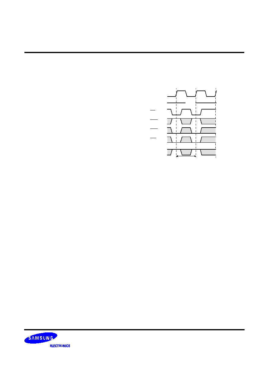
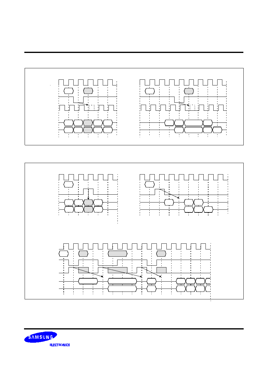
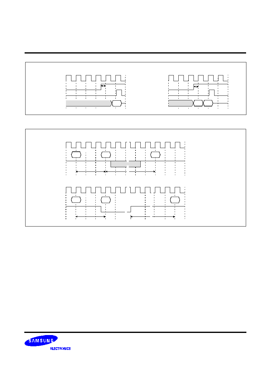
2. DQM Operation
WR
D
0
D
1
D
3
D
0
D
1
D
3
CLK
CMD
DQMi
Note 1
DQ(CL2)
DQ(CL3)
Masked by DQM
2) Read Mask (BL=4)
RD
Q
0
Q
2
Q
3
Q
1
Q
2
Q
3
Masked by DQM
DQM to Data-in Mask = 0CLK
DQM to Data-out Mask = 2CLK
Hi-Z
Hi-Z
3) DQM with Clock Suspended (Full Page Read)
Note 2
RD
CLK
CMD
CKE
DQ(CL2)
DQ(CL3)
Q
0
Q
4
Q
7
Q
8
Q
2
Q
3
Q
6
Q
7
Q
1
Hi-Z
Hi-Z
Hi-Z
Hi-Z
Hi-Z
Hi-Z
DQM
*Note : 1. There are 4 DQMi(i=0~3).
Each DQMi masks 8 DQi
s.(1 Byte, 1 Pixel for 8 bpp)
2. DQM makes data out Hi-Z after 2 clocks which should masked by CKE " L".
Q
6
Q
5
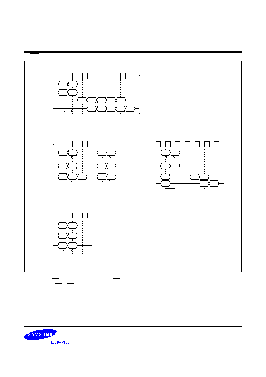
1) Clock Suspended During Write (BL=4)
1. CLOCK Suspend
WR
D
0
D
1
D
2
D
3
D
0
D
1
D
2
D
3
CLK
CMD
CKE
Internal
CLK
DQ(CL2)
DQ(CL3)
Masked by CKE
2) Clock Suspended During Read (BL=4)
D
0
Not Written
BASIC FEATURE AND FUNCTION DESCRIPTIONS
RD
Q
0
Q
1
Q
2
Q
0
Q
1
Q
2
Q
3
Masked by CKE
Q
3
Suspended Dout
Note : CKE to CLK disable/enable=1 clock
K4G323222M
CMOS SGRAM
Rev. 1.1 (Feb. 2000)
t
CCD Note 2
t
CDL
Note 3
t
CCD Note 2
t
CDL
Note 3
1. By " Interrupt ", It is possible to stop burst read/write by external command before the end of burst.
By "CAS Interrupt" , to stop burst read/write by CAS access ; read, write and block write.
2. t
CCD
: CAS to CAS delay. (=1CLK)
3. t
CDL
: Last data in to new column address delay. (=1CLK)
4. Pixel :Pixel mask.
5. t
BWC
: Block write minimum cycle time.
DQ(CL2)
DQ(CL3)
t
CCD Note 2
t
CDL
Note 3
Note 4
t
BWC
Note 5
Note 4
Note 2
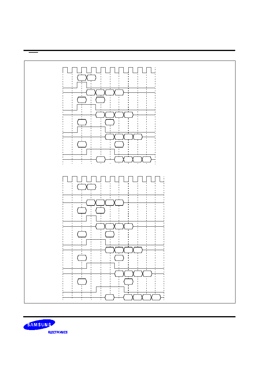
3. CAS Interrupt (I)
1) Read interrupted by Read (BL=4)
Note 1
CLK
CMD
ADD
2) Write interrupted by(Block) Write (BL=2)
3) Write interrupted by Read (BL=2)
DQ(CL2)
DQ(CL3)
4) Block Write to Block Write
CLK
CMD
ADD
DQ
RD
RD
A
B
QA
0
QA
0
QB
0
QB
0
QB
1
QB
2
QB
3
QB
1
QB
2
QB
3
t
CCD
A
B
C
D
WR
WR
WR
BW
DA
0
DB
0
DB
1
DC
0
Pixel
DA
0
DA
0
QB
0
QB
1
QB
0
QB
1
A
B
WR
RD
A
B
Pixel
Pixel
BW
BW
*Note :
CLK
CMD
ADD
DQ
K4G323222M
CMOS SGRAM
Rev. 1.1 (Feb. 2000)
RD
WR
D
1
D
2
D
3
D
0
1. To prevent bus contention, there should be at least one gap between data in and data out.
2. To prevent bus contention, DQM should be issued which makes at least one gap between data in and data out.
RD
WR
RD
WR
Hi-Z
Hi-Z
D
1
D
2
RD
D
3
WR
D
0
D
1
D
2
D
3
D
0
D
1
D
2
D
3
D
0
RD
WR
RD
WR
RD
WR
D
1
D
2
D
3
D
0
Hi-Z
Q
0
D
1
D
2
D
3
D
0
Note 1
RD
WR
Hi-Z
D
1
D
2
D
3
D
0
RD
WR
Q
0
D
1
D
2
D
3
D
0
Note 2
Hi-Z
v) CMD
DQM
DQ
DQM
DQ
DQM
DQ
DQM
DQ
DQM
DQ
(2) CL=3, BL=4
CLK
i) CMD
ii) CMD
iii) CMD
iv) CMD
*Note :
DQM
DQ
DQM
DQ
iv) CMD
iii) CMD
DQM
DQ
DQM
DQ
CLK
(1) CL=2, BL=4
i) CMD
ii) CMD
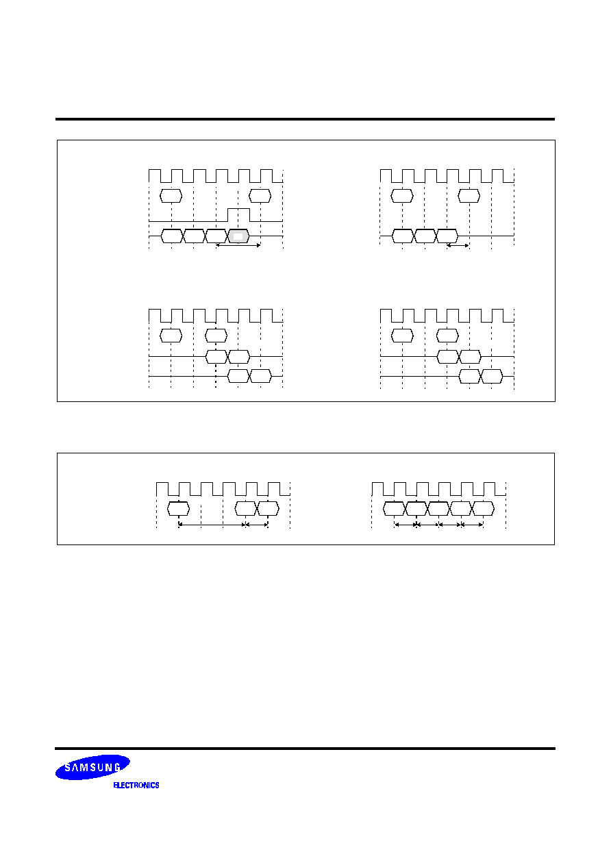
4. CAS Interrupt (II) : Read Interrupted by Write & DQM
D
0
D
1
D
2
D
3

K4G323222M
CMOS SGRAM
Rev. 1.1 (Feb. 2000)
Note 3
Auto Precharge Starts
*Note : 1. To inhibit invalid write, DQM should be issued.
2. This precharge command and burst write command should be of the same bank, otherwise it is not precharge
interrupt but only another bank precharge of dual banks operation.
3. For -55/60/70/80, tRDL=1CLK product can be supported within restricted amounts and it will be distinguished by bucket code "NV"
. From the next generation, tRDL will be only 2CLK for every clock frequency.
5. Write Interrupted by Precharge & DQM
D
0
D
1
D
2
CLK
CMD
DQM
DQ
Masked by DQM
WR
PRE
D
3
Note 2,3
Note 1
*Note :1. t
BPL
: Block write data-in to PRE command delay
2. Number of valid output data after Row Precharge : 1, 2 for CAS Latency =2, 3 respectively.
3. The row active command of the precharge bank can be issued after t
RP
from this point. The new read/write command of other activated
bank can be issued from this point. At burst read/write with auto precharge, CAS interrupt of the same/another bank is illegal.
4. For -55/60/70/80, tRDL=1CLK product can be supported within restricted amounts and it will be distinguished by bucket code "NV"
. From the next generation, tRDL will be only 2CLK for every clock frequency.
6. Precharge
D
0
D
1
D
2
CLK
CMD
DQ
WR
PRE
D
3
1) Normal Write (BL=4)
t
RDL
Note 1,4
3) Read (BL=4)
CLK
CMD
DQ(CL2)
DQ(CL3)
RD
PRE
Q
0
Q
1
Q
2
Q
3
Q
0
Q
1
Q
2
Q
3
1
2
Note 2
7. Auto Precharge
D
0
D
1
D
2
CLK
CMD
DQ
WR
D
3
1) Normal Write (BL=4)
Note 3,4
Auto Precharge Starts
3) Read (BL=4)
CLK
CMD
DQ(CL2)
DQ(CL3)
RD
Q
0
Q
1
Q
2
Q
3
Q
0
Q
1
Q
2
Q
3
Note 3
Auto Precharge Starts
Pixel
CLK
CMD
DQ
BW
PRE
2) Block Write
t
BPL
Note 1
CLK
CMD
DQ
(CL 2, 3)
2) Block Write
Pixel
BW
t
BPL
t
RP
K4G323222M
CMOS SGRAM
Rev. 1.1 (Feb. 2000)
1. t
RDL
: 1 CLK, Last Data in to Row Precharge.
2. t
BDL
: 1 CLK, Last Data in to Burst Stop Delay.
3. Number of valid output data after Row precharge or burst stop : 1, 2 for CAS latency= 2, 3 respectiviely.
4. PRE : Both banks precharge if necessary.
MRS can be issued only at all bank precharge state.
5. For -55/60/70/80, tRDL=1CLK product can be supported within restricted amounts and it will be distinguished by bucket code "NV"
. From the next generation, tRDL will be only 2CLK for every clock frequency.
D
3
t
RDL Note 1,5
Note 3
Note 3
t
BDL
Note 4
8. Burst Stop & Precharge Interrupt
1) Write Interrupted by Precharge (BL=4)
2) Write Burst Stop (Full Page Only)
3) Read Interrupted by Precharge (BL=4)
4) Read Burst Stop (Full Page Only)
CLK
CMD
DQ(CL2)
DQ(CL3)
CLK
CMD
DQ(CL2)
DQ(CL3)
9. MRS & SMRS
1) Mode Register Set
2) Special Mode Register Set
CLK
CMD
CLK
CMD
*Note :
t
RP
1CLK
1CLK
1CLK
1CLK
1CLK
CLK
CMD
DQM
DQ
CLK
CMD
DQ
WR
PRE
D
0
D
1
D
2
PRE
RD
Q
0
Q
1
Q
0
Q
1
1
2
Q
0
Q
1
1
Q
0
Q
1
2
STOP
RD
PRE
MRS ACT
SMRS ACT SMRS SMRS BW
D
0
D
1
D
2
WR
STOP
K4G323222M
CMOS SGRAM
Rev. 1.1 (Feb. 2000)
1. Active power down : one or more bank active state.
2. Precharge power down : both bank precharge state.
3. The auto refresh is the same as CBR refresh of conventional DRAM.
No precharge commands are required after Auto Refresh command.
During tRC from auto refresh command, any other command can not be accepted.
4. Before executing auto/self refresh command, both banks must be idle state.
5. (S)MRS, Bank Active, Auto/Self Refresh, Power Down Mode Entry.
6. During self refresh mode, refresh interval and refresh operation are perfomed internally.
After self refresh entry, self refresh mode is kept while CKE is LOW.
During self refresh mode, all inputs expect CKE will be don
t cared, and outputs will be in Hi-Z state.
During tRC from self refresh exit command, any other command can not be accepted.
Before/After self refresh mode, burst auto refresh cycle (2K cycles) is recommended.
t
SS
Note 1
Note 5
Internal
CLK
t
SS
Note 2
Note 4
t
RP
t
RC
Note 4
t
RP
t
RC
10. Clock Suspend Exit & Power Down Exit
1) Clock Suspend (=Active Power Down) Exit
2) Power Down (=Precharge Power Down) Exit
CLK
CKE
CMD
Internal
CLK
CLK
CKE
CMD
11. Auto Refresh & Self Refresh
1) Auto Refresh
Note 3
2) Self Refresh
Note 6
CLK
CMD
CKE
CLK
CMD
CKE
*Note :
RD
NOP ACT
CMD
SR
PRE
CMD
AR
PRE
K4G323222M
CMOS SGRAM
Rev. 1.1 (Feb. 2000)
12. About Burst Type Control
Basic
MODE
Sequential Counting
At MRS A
3
= "0". See the BURST SEQUENCE TABLE. (BL=4,8)
BL=1, 2, 4, 8 and full page wrap around.
Interleave Counting
At MRS A
3
= "1". See the BURST SEQUENCE TABLE. (BL=4,8)
BL=4, 8. At BL=1, 2 Interleave Counting = Sequential Counting
Pseudo-
MODE
Pseudo-
Decrement Sequential
Counting
At MRS A
3
= "1".(See to Interleave Counting Mode)
Starting Address LSB 3 bits A
0-2
should be "000" or "111".@BL=8.
-- if LSB="000" : Increment Counting.
-- if LSB="111" : Decrement Counting.
For Example,(Assume Addresses except LSB 3 bits are all 0, BL=8)
-- @ write, LSB="000", Accessed Column in order 0-1-2-3-4-5-6-7
-- @ read, LSB="111", Accessed Column in order 7-6-5-4-3-2-1-0
At BL=4, same applications are possible. As above example, at Interleave Counting mode,
by confining starting address to some values, Pseudo-Decrement Counting Mode can be
realized. See the BURST SEQUENCE TABLE carefully.
Pseudo-
Binary Counting
At MRS A
3
= "0".(See to Sequential Counting Mode)
A
0-2
= "111".(See to Full Page Mode)
Using Full Page Mode and Burst Stop Command, Binary Counting Mode can be realized.
-- @ Sequential Counting, Accessed Column in order 3-4-5-6-7-1-2-3(BL=8)
-- @ Pseudo-Binary Counting,
Accessed Column in order 3-4-5-6-7-8-9-10(Burst Stop command)
Note. The next column address of 256 is 0.
Random
MODE
Random column Access
t
CCD
= 1 CLK
Every cycle Read/Write Command with random column address can realize
Random Column Access.
That is similar to Extended Data Out (EDO) Operation of conventional DRAM.
13. About Burst Length Control
Basic
MODE
1
At MRS A
2,1,0
= "000".
At auto precharge, t
RAS
should not be violated.
2
At MRS A
2,1,0
= "001".
At auto precharge, t
RAS
should not be violated.
4
At MRS A
2,1,0
= "010".
8
At MRS A
2,1,0
= "011".
Full Page
At MRS A
2,1,0
= "111".
Wrap around mode(Infinite burst length)should be stopped by burst stop,
RAS interrupt or CAS interrupt.
Special
MODE
BRSW
At MRS A
9
= "1".
Read burst =1, 2, 4, 8, full page/write Burst =1
At auto precharge of write, t
RAS
should not be violated.
Block Write
8 Column Block Write. LSB A0-2 are ignored. Burst length=1.
t
BWC
should not be violated.
At auto precharge, t
RAS
should not be violated.
Random
MODE
Burst Stop
t
BDL
= 1, Valid DQ after burst stop is 1, 2 for CL=2, 3 respectively
Using burst stop command, it is possible only at full page burst length.
Interrupt
MODE
RAS Interrupt
(Interrupted by Precharge)
Before the end of burst, Row precharge command of the same bank
stops read/write burst with Row precharge.
t
RDL
= 2 with DQM, valid DQ after burst stop is 1, 2 for CL= 2, 3 respectively
During read/write burst with auto precharge, RAS interrupt cannot be issued.
CAS Interrupt
Before the end of burst, new read/write stops read/write burst and starts new
read/write burst or block write.
During read/write burst with auto precharge, CAS interrupt can not be issued.
K4G323222M
CMOS SGRAM
Rev. 1.1 (Feb. 2000)
I/O(=DQ)
31 24
23 16
15 8
7 0
External Data-in
1 1 1 1 1 1 1 1
1 1 1 1 1 1 1 1
0 0 0 0 0 0 0 0
0 0 0 0 0 0 0 0
DQMi
DQM
3
=0
DQM
2
=0
DQM
1
=0
DQM
0
=1
Mask Register
0 1 1 1 1 1 1 0
1 0 1 1 1 1 1 1
0 1 1 1 1 1 0 1
0 1 1 1 0 1 1 0
Before Write
0 0 0 0 0 0 0 0
0 0 0 0 0 0 0 0
1 1 1 1 1 1 1 1
1 1 1 1 1 1 1 1
After Write
0 1 1 1 1 1 1 0
1 0 1 1 1 1 1 1
1 0 0 0 0 0 1 0
1 1 1 1 1 1 1 1
14. Mask Functions
1) Normal Write
I/O masking : By Mask at Write Per Bit Mode, the selected bit planes keep the original data.
If bit plane 0, 3, 7, 9, 15, 22, 24, and 31 keep the original value.
i) STEP
- SMRS(LMR) :Load mask[31-0]="0111, 1110, 1011,1111, 0111, 1101, 0111, 0110"
- Row Active with DSF "H" :Write Per Bit Mode Enable
- Perform Normal Write.
i) ILLUSTRATION
I/O(=DQ)
31 24
23 16
15 8
7 0
DQMi
DQM
3
=0
DQM
2
=0
DQM
1
=0
DQM
0
=1
Color Register
Color3=Blue
Color2=Green
Color1=Yellow
Color0=Red
Before
Block
Write
&
DQ
(Pixel
data)
000
White DQ
24
=H
White DQ
16
=H
White DQ
8
=H
White DQ
0
=L
001
White DQ
25
=H
White DQ
17
=H
White DQ
9
=L
White DQ
1
=H
010
White DQ
26
=H
White DQ
18
=L
White DQ
10
=H
White DQ
2
=H
011
White DQ
27
=L
White DQ
19
=H
White DQ
11
=H
White DQ
3
=H
100
White DQ
28
=H
White DQ
20
=H
White DQ
12
=H
White DQ
4
=L
101
White DQ
29
=H
White DQ
21
=H
White DQ
13
=L
White DQ
5
=H
110
White DQ
30
=H
White DQ
22
=L
White DQ
14
=H
White DQ
6
=H
111
White DQ
31
=L
White DQ
23
=H
White DQ
15
=H
White DQ
7
=H
After
Block
Write
000
Blue
Green
Yellow
White
001
Blue
Green
White
White
010
Blue
White
Yellow
White
011
White
Green
Yellow
White
100
Blue
Green
Yellow
White
101
Blue
Green
White
White
110
Blue
White
Yellow
White
111
White
Green
Yellow
White
2) Block Write
Pixel masking : By Pixel Data issued through DQ pin, the selected pixels keep the original data.
See PIXEL TO DQ MAPPING TABLE.
If Pixel 0, 4, 9, 13, 18, 22, 27 and 31 keep the original white color.
Assume 8bpp,
White = "0000,0000", Red="1010,0011", Green = "1110,0001", Yellow = "0000,1111", Blue = "1100,0011"
i) STEP
- SMRS(LCR) :Load color(for 8bpp, through x32 DQ color0-3 are loaded into color registers)
Load(color3, color2, color1, color0) = (Blue, Green, Yellow, Red)
= "1100,0011, 1110, 0001, 0000, 1111, 1010, 0011"
- Row Active with DSF "L" : I/O Mask by Write Per Bit Mode Disable
- Block write with DQ[31-0] = "0111, 0111, 1011, 1011, 1101, 1101, 1110, 1110"
i) ILLUSTRATION
1. DQM byte masking.
2. At normal write, ONE column is selected among columns decorded by A
2-0
(000-111).
At block write, instead of ignored address A
2-0
, DQ
0-31
control each pixel.
Note 1
Note 2
*Note :
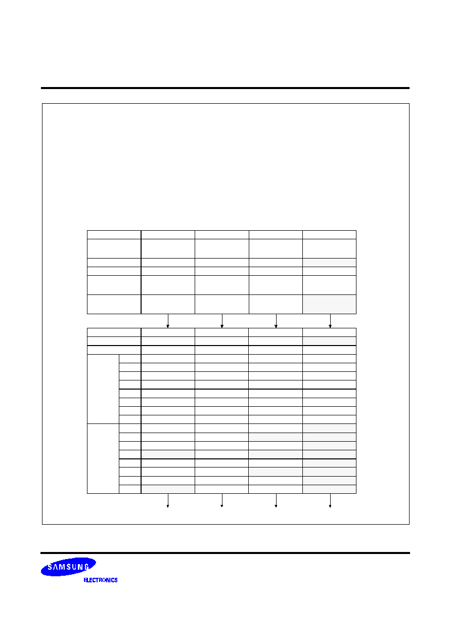
K4G323222M
CMOS SGRAM
Rev. 1.1 (Feb. 2000)
I/O(=DQ)
31 24
23 16
15 8
7 0
Color Register
Blue
1 1 0 0 0 0 1 1
Green
1 1 1 0 0 0 0 1
Yellow
0 0 0 0 1 1 1 1
Red
1 0 1 0 0 0 1 1
DQMi
DQM
3
=0
DQM
2
=0
DQM
1
=0
DQM
0
=1
Mask Register
1 1 1 1 1 1 1 1
1 1 0 1 1 1 0 1
0 1 0 0 0 0 1 0
0 1 1 1 0 1 1 0
Before Write
Yellow
0 0 0 0 1 1 1 1
Yellow
0 0 0 0 1 1 1 1
Green
1 1 1 0 0 0 0 1
White
0 0 0 0 0 0 0 0
After Write
Blue
1 1 0 0 0 0 1 1
Blue
1 1 0 0 0 0 1 1
Red
1 0 1 0 0 0 1 1
White
0 0 0 0 0 0 0 0
(Continued)
Pixel and I/O masking : By Mask at Write Per Bit Mode, the selected bit planes keep the original data.
By Pixel Data issued through DQ pin, the selected pixels keep the original data.
See PIXEL TO DQ MAPPING TABLE.
Assume 8bpp,
White = "0000,0000", Red="1010,0011", Green ="1110,0001", Yellow ="0000,1111", Blue ="1100,0011"
i) STEP
- SMRS(LCR) : Load color(for 8bpp, through x 32 DQ color0-3 are loaded into color registers)
Load(color3, color2, color1, color0) = (Blue, Green, Yellow, Red)
= "1100,0011,1110,0001,0000,1111,1010,0011"
- SMRS(LMR ): Load mask. Mask[31-0] ="1111,1111,1101,1101, 0100,0010,0111,0110"
--> Byte 3 : No I/O Masking ; Byte 2 : I/O Masking ; Byte 1 : I/O and Pixel Masking ; Byte 0 : DQM Byte Masking
- Row Active with DSF "H" : I/O Mask by Write Per Bit Mode Enable
- Block Write with DQ[31-0] = "0111,0111,1111,1111,0101,0101,1110,1110" (Pixel Mask)
i) ILLUSTRATION
Note 2 Note 1
I/O(=DQ)
31 24
23 16
15 8
7 0
DQMi
DQM
3
=0
DQM
2
=0
DQM
1
=0
DQM
0
=1
Color Register
Color3=Blue
Color2=Green
Color1=Yellow
Color0=Red
Before
Block
Write
&
DQ
(Pixel
data)
000
Yellow DQ
24
=H
Yellow DQ
16
=H
Green DQ
8
=H
White DQ
0
=L
001
Yellow DQ
25
=H
Yellow DQ
17
=H
Green DQ
9
=L
White DQ
1
=H
010
Yellow DQ
26
=H
Yellow DQ
18
=H
Green DQ
10
=H
White DQ
2
=H
011
Yellow DQ
27
=L
Yellow DQ
19
=H
Green DQ
11
=L
White DQ
3
=H
100
Yellow DQ
28
=H
Yellow DQ
20
=H
Green DQ
12
=H
White DQ
4
=L
101
Yellow DQ
29
=H
Yellow DQ
21
=H
Green DQ
13
=L
White DQ
5
=H
110
Yellow DQ
30
=H
Yellow DQ
22
=H
Green DQ
14
=H
White DQ
6
=H
111
Yellow DQ
31
=L
Yellow DQ
23
=H
Green DQ
15
=L
White DQ
7
=H
After
Block
Write
000
Blue
Blue
Red
White
001
Blue
Blue
Green
White
010
Blue
Blue
Red
White
011
Yellow
Blue
Green
White
100
Blue
Blue
Red
White
101
Blue
Blue
Green
White
110
Blue
Blue
Red
White
111
Yellow
Blue
Green
White
1. DQM byte masking.
2. At normal write, ONE column is selected among columns decorded by A
2-0
(000-111).
At block write, instead of ignored address A
2-0
, DQ
0-31
control each pixel.
PIXEL MASK
I/O MASK
PIXEL & I/O MASK
BYTE MASK
*Note :
Note 1
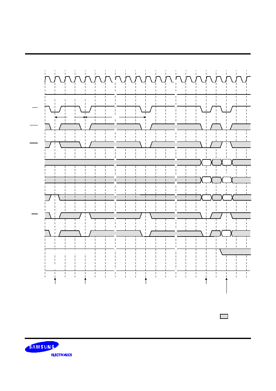
K4G323222M
CMOS SGRAM
Rev. 1.1 (Feb. 2000)
0
1
2
3
4
5
6
7
8
9
10
11
12
13
14
15
16
17
18
19
Power On Sequence & Auto Refresh
CLOCK
CKE
CS
RAS
CAS
ADDR
BA
A
8
/AP
DQ
WE
DQM
Ra
tRP
tRC
High level is necessary
High-Z
High level is necessary
: Don
t care
Precharge
Auto Refresh
Auto Refresh
Mode Register Set
(All Banks)
DSF
Ra
BS
KEY
KEY
KEY
Row Active
(Write per Bit
Enable or Disable)
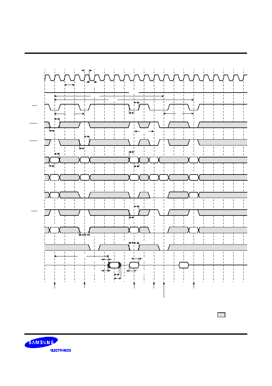
K4G323222M
CMOS SGRAM
Rev. 1.1 (Feb. 2000)
0
1
2
3
4
5
6
7
8
9
10
11
12
13
14
15
16
17
18
19
*Note 5
Row Active
Read
Write
Read
Row Active
Precharge
Single Bit Read-Write-Read Cycle(Same Page) @CAS Latency=3, Burst Length=1
t
RCD
*Note 1
t
SS
t
SH
t
RP
t
CCD
t
SS
t
SH
t
RAC
t
SAC
t
SLZ
t
SH
t
SH
t
SS
t
SS
t
SH
t
SS
t
SH
CLOCK
CKE
CS
RAS
CAS
ADDR
BA
A
8
/AP
DQ
WE
DQM
HIGH
t
SH
t
SH
t
SS
t
SS
*Note 2,3
*Note 2,3 *Note 4
*Note 4
*Note 3
*Note 3
*Note 3
Rb
Cc
Cb
Ca
Ra
BS
BS
BS
BS
BS
BS
Ra
Rb
Qc
Db
Qa
*Note 2,3
*Note 2
*Note 2
t
SS
t
SH
DSF
*Note 5
*Note 6
*Note 3
t
CH
t
CC
t
CL
t
RAS
t
RC
t
SS
t
OH
t
SHZ
(Write per Bit
Enable or
Disable)
or
Block Write
(Write per Bit
Enable or Disable)
: Don
t care
K4G323222M
CMOS SGRAM
Rev. 1.1 (Feb. 2000)
1. All input can be don't care when CS is high at the CLK high going edge.
2. Bank active & read/write are controlled by BA.
BA
Active & Read/Write
0
Bank A
1
Bank B
A
8
/AP
BA
Operation
0
0
Disable auto precharge, leave bank A active at end of burst.
1
Disable auto precharge, leave bank B active at end of burst.
1
0
Enable auto precharge, precharge bank A at end of burst.
1
Enable auto precharge, precharge bank B at end of burst.
A
8
/AP
BA
Precharge
0
0
Bank A
0
1
Bank B
1
X
Both Bank
BA
DSF
Operation
0
L
Bank A row active, disable write per bit function for bank A
H
Bank A row active, enable write per bit function for bank A
1
L
Bank B row active, disable write per bit function for bank B
H
Bank B row active, enable write per bit function for bank B
DSF
Operation
Minimum cycle time
L
Normal write
t
CCD
H
Block write
t
BWC
3. Enable and disable auto precharge function are controlled by A
8
/AP in read/write command.
4. A
8
/AP and BA control bank precharge when precharge command is asserted.
5. Enable and disable Write-per Bit function are controlled by DSF in Row Active command.
6. Block write/normal write is controlled by DSF.
*Note :
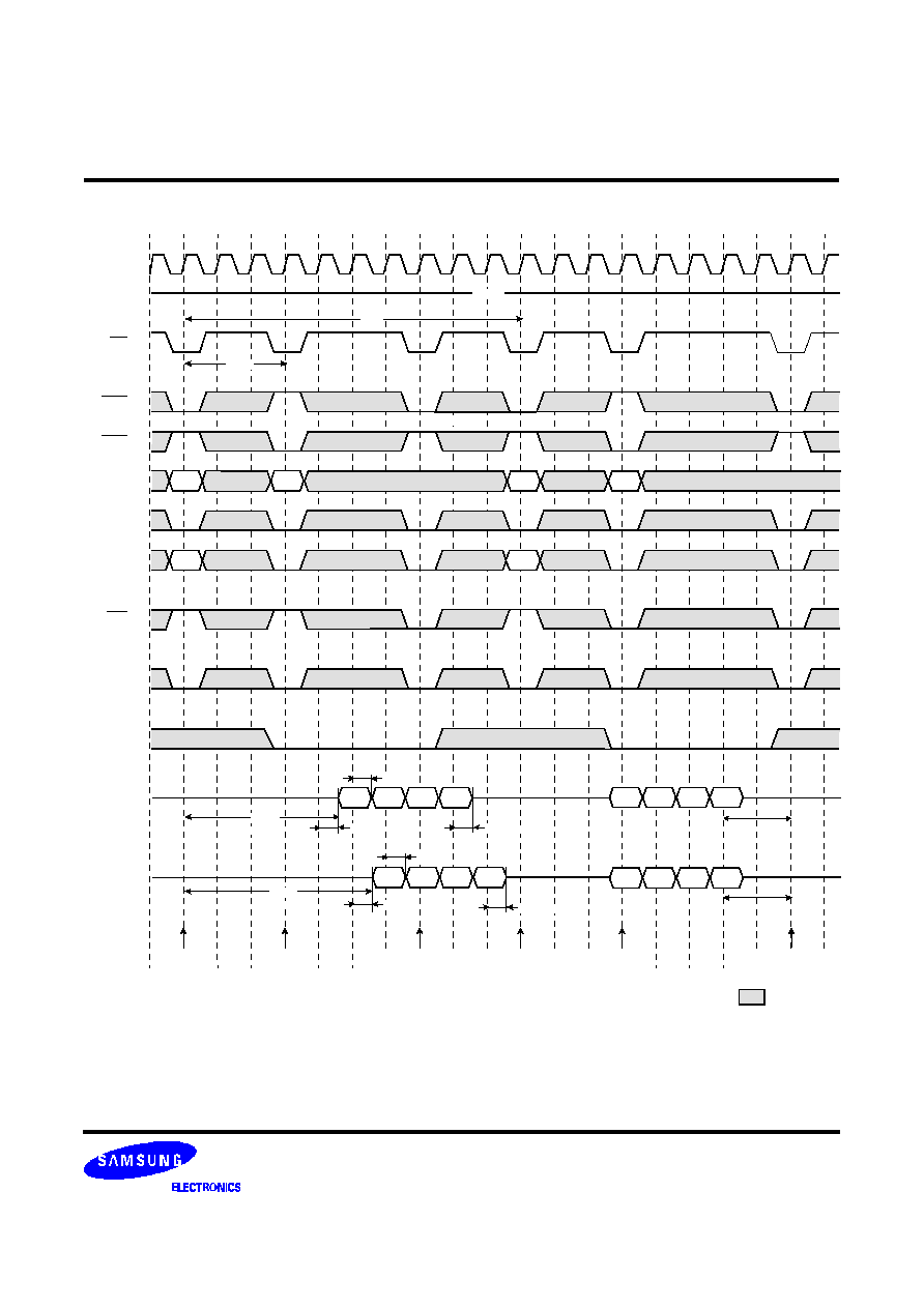
K4G323222M
CMOS SGRAM
Rev. 1.1 (Feb. 2000)
0
1
2
3
4
5
6
7
8
9
10
11
12
13
14
15
16
17
18
19
Read & Write Cycle at Same Bank @Burst Length=4
HIGH
Row Active
(A-Bank)
Precharge
(A-Bank)
Row Active
(A-Bank)
Write
(A-Bank)
Precharge
(A-Bank)
*Note :
1. Minimum row cycle times is required to complete internal DRAM operation.
2. Row precharge can interrupt burst on any cycle. [CAS Latency - 1] valid output data available after Row
enters precharge. Last valid output will be Hi-Z after
t
SHZ
from the clcok.
3. Access time from Row address.
t
CC
*(
t
RCD
+ CAS latency - 1) +
t
SAC
4. Ouput will be Hi-Z after the end of burst. (1, 2, 4, & 8). At Full page bit burst, burst is wrap-around.
5. For -55/60/70/80, tRDL=1CLK product can be supported within restricted amounts and it will be distinguished by bucket code
"NV". From the next generation, tRDL will be only 2CLK for every clock frequency.
Read
(A-Bank)
*Note 1
t
RC
t
RCD
*Note 2
t
RDL
t
RDL
t
SHZ
*Note 4
t
SHZ
*Note 4
t
OH
t
RAC
*Note 3
t
SAC
t
SAC
t
RAC
*Note 3
t
OH
BA
A
8
/AP
ADDR
CAS
RAS
CS
CKE
CLOCK
Ra
Rb
Qa0
Qa1
Qa2
Qa3
Qa0
Qa1
Qa2
Qa3
Db0
Db1
Db2
Db3
Db0
Db1
Db2
Db3
Ra
Ca0
Rb
Cb0
WE
DQM
DSF
: Don
t care
(CL=2)
(CL=3)
DQ
DQ
*Note 5
*Note 5
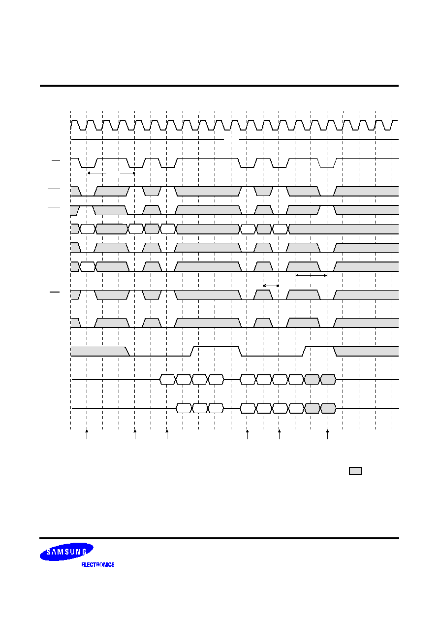
K4G323222M
CMOS SGRAM
Rev. 1.1 (Feb. 2000)
0
1
2
3
4
5
6
7
8
9
10
11
12
13
14
15
16
17
18
19
*Note 3
Page Read & Write Cycle at Same Bank @Burst Length=4
HIGH
Row Active
(A-Bank)
Read
(A-Bank)
Write
(A-Bank)
Precharge
(A-Bank)
1. To write data before burst read ends, DQM should be asserted three cycle prior to write command to avoid bus contention.
2. Row precharge will interrupt writing. Last data input,
t
RDL
before Row precharge, will be written.
3. DQM should mask invalid input data on precharge command cycle when asserting precharge
before end of burst. Input data after Row precharge cycle will be masked internally.
4. For -55/60/70/80, tRDL=1CLK product can be supported within restricted amounts and it will be distinguished by bucket code
"NV". From the next generation, tRDL will be only 2CLK for every clock frequency.
Read
(A-Bank)
t
RCD
*Note 2
*Note 1
t
CDL
Qa0
Qa1
Qb0
Qb1
Qa0
Qa1
Qb0
Dc0
Dc1
Dd0
Dd1
Dc0
Dc1
Dd0
Dd1
Write
(A-Bank)
BA
A
8
/AP
ADDR
CAS
RAS
CS
CKE
CLOCK
WE
DQM
Ra
Ca0
Cb0
Cc0
Cd0
Ra
DSF
t
RDL
*Note 2
: Don
t care
*Note :
(CL=2)
(CL=3)
DQ
DQ
*Note 4
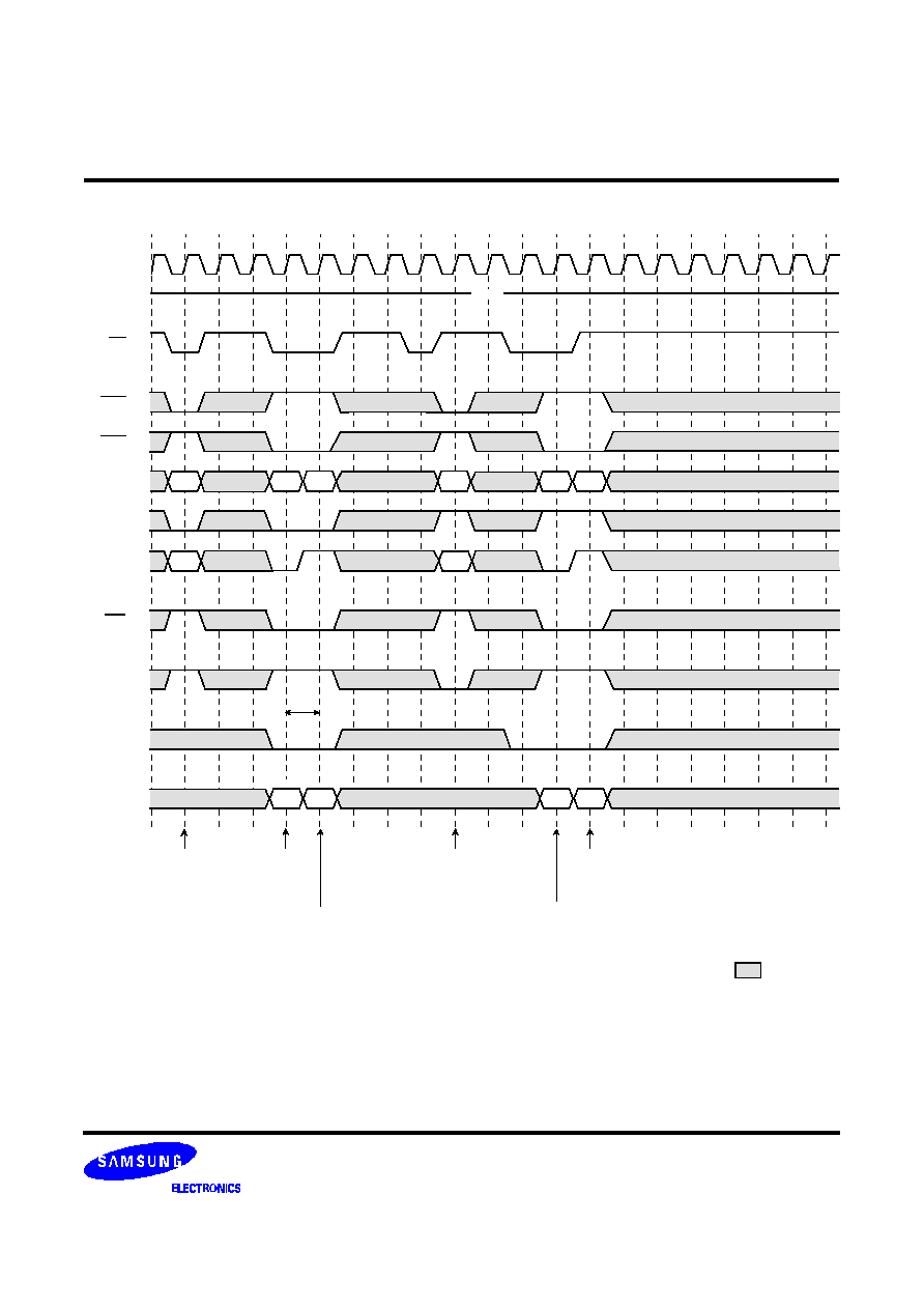
K4G323222M
CMOS SGRAM
Rev. 1.1 (Feb. 2000)
0
1
2
3
4
5
6
7
8
9
10
11
12
13
14
15
16
17
18
19
Block Write cycle(with Auto Precharge)
HIGH
Row Active with
Write-per-Bit
Enable
(A-Bank)
Masked
Block Write with
Auto Precharge
(A-Bank)
Block Write
(B-Bank)
Row Active
(B-Bank)
1. Column Mask(DQi=L : Mask, DQi=H :Non Mask)
2. At Block Write, CA
0~2
are ignored.
Masked
Block Write
(A-Bank)
t
BWC
Block Write with
Auto Precharge
(B-Bank)
BA
A
8
/AP
ADDR
CAS
RAS
CS
CKE
CLOCK
WE
DQM
RAa
CAa
CAb
CBa
CBb
RAa
DSF
RBa
RBa
DQ
Pixel
Mask
Pixel
Mask
Pixel
Mask
Pixel
Mask
*Note 1
*Note 2
*Note :
: Don
t care
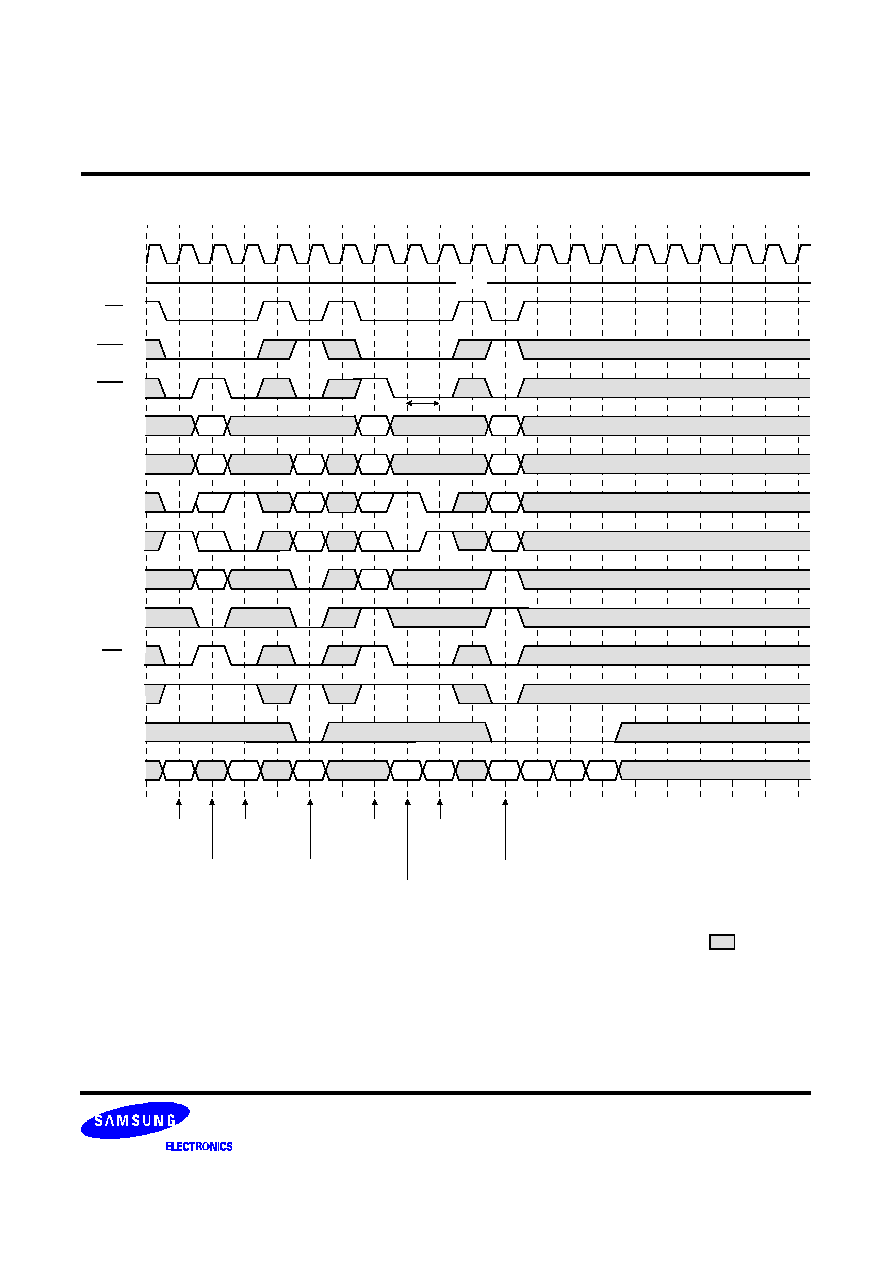
K4G323222M
CMOS SGRAM
Rev. 1.1 (Feb. 2000)
0
1
2
3
4
5
6
7
8
9
10
11
12
13
14
15
16
17
18
19
SMRS and Block/Normal Write @ Burst Length=4
HIGH
Load Color
Register
Masked
Block Write
(A-Bank)
Load Color
Register
Row Active
with WPB*
Enable
(B-Bank)
Load Mask
Register
*Note 1
Masked Write
with Auto
Precharge
(B-Bank)
A
3,4,7,8
A
5
A
0-2
CAS
RAS
CS
CKE
CLOCK
WE
DQM
RAa
RBa
CBa
DSF
DQ
A
8
/AP
BA
A
6
RAa
RBa
CBa
CAa
RAa
RBa
CBa
CAa
RAa
RBa
CBa
CAa
RAa
RBa
Color
I/O
Mask
Pixel
Mask
I/O
Mask
Color
DBa0 DBa1 DBa2 DBa3
Row Active
with WPB*
Enable
(A-Bank)
*Note : 1. At the next clock of special mode set command, new command is possible.
Load Mask Register
WPB* : Write-Per-Bit
: Don
t care
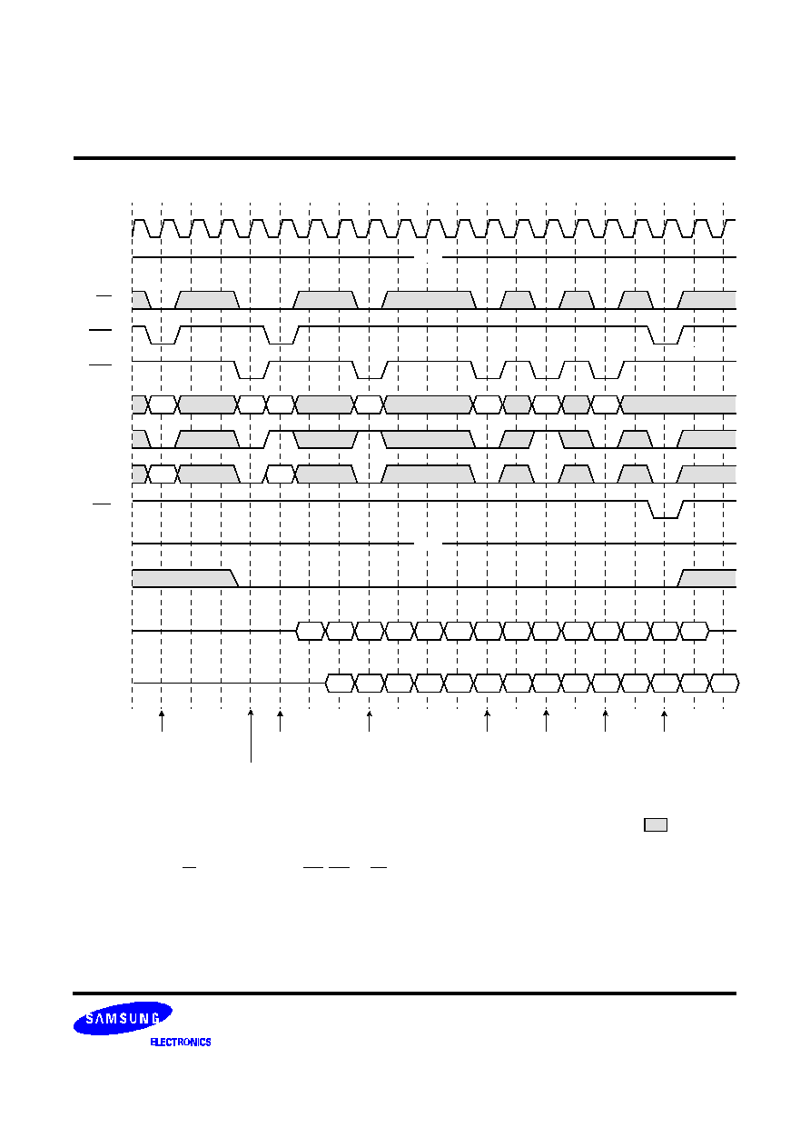
K4G323222M
CMOS SGRAM
Rev. 1.1 (Feb. 2000)
0
1
2
3
4
5
6
7
8
9
10
11
12
13
14
15
16
17
18
19
Page Read Cycle at Different Bank @Burst Length=4
HIGH
Row Active
(A-Bank)
Row Active
(B-Bank)
Read
(A-Bank)
Read
(B-Bank)
1. CS can be don
t care when RAS, CAS and WE are high at the clock high going edge.
2. To interrupt a burst read by row precharge, both the read and the precharge banks must be the same.
Read
(A-Bank)
*Note 2
*Note 1
Read
(B-Bank)
Read
(A-Bank)
Precharge
(A-Bank)
BA
A
8
/AP
ADDR
CAS
RAS
CS
CKE
CLOCK
WE
DQM
RAa
RBb
RAa
RBb
CAa
CBb
CBd
CAc
CAe
QAa0 QAa1
QAa2 QAa3
QBb0 QBb1 QBb2 QBb3
QAc0
QAc1
QBd0 QBd1
QAe0 QAe1
QAa0 QAa1
QAa2 QAa3
QBb0 QBb1 QBb2 QBb3
QAc0
QAc1
QBd0 QBd1
QAe0 QAe1
DSF
LOW
*Note :
: Don
t care
(CL=2)
(CL=3)
DQ
DQ
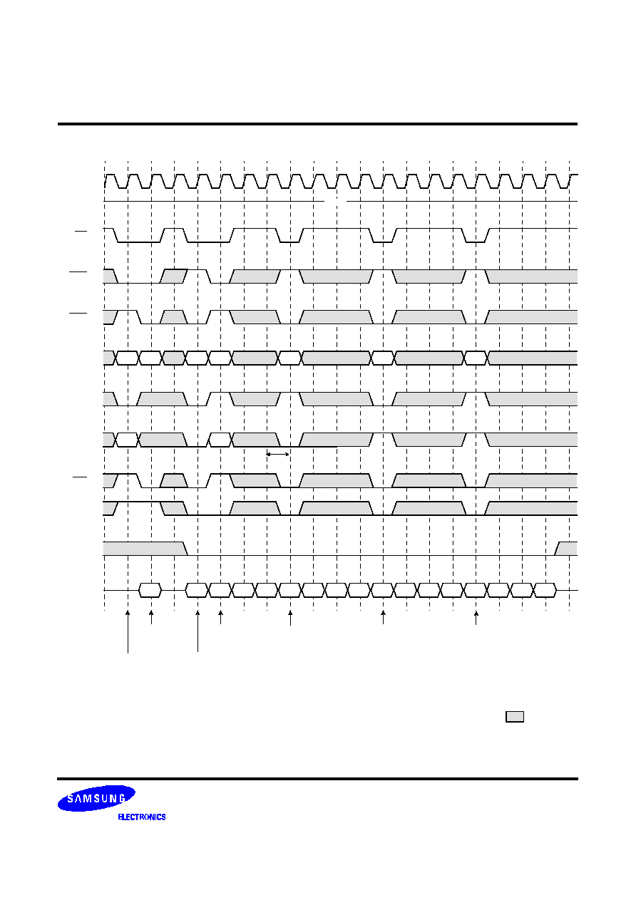
K4G323222M
CMOS SGRAM
Rev. 1.1 (Feb. 2000)
0
1
2
3
4
5
6
7
8
9
10
11
12
13
14
15
16
17
18
19
Page Write Cycle at Different Bank @Burst Length=4
HIGH
Row Active with
Write-Per-Bit
enable
(A-Bank)
Row Active
(B-Bank)
Masked Write
with auto
precharge
(A-Bank)
Masked Write
(A-Bank)
Write with auto
Precharge
(B-Bank)
t
CDL
Write
(B-Bank)
BA
DQ
ADDR
CAS
RAS
CS
CKE
CLOCK
WE
DQM
A
8
/AP
RAa
CAa
CBb
CAc
RAa
DAa0 DAa1 DAa2
DAa3
DBb0
DBb1
DBb2 DBb3
DAc0
DAc1
DAc2
DAc3
RBb
RBb
Key
CBd
DSF
Mask
DBd0
DBd1
DBd2
DBd3
Load Mask
Register
: Don
t care
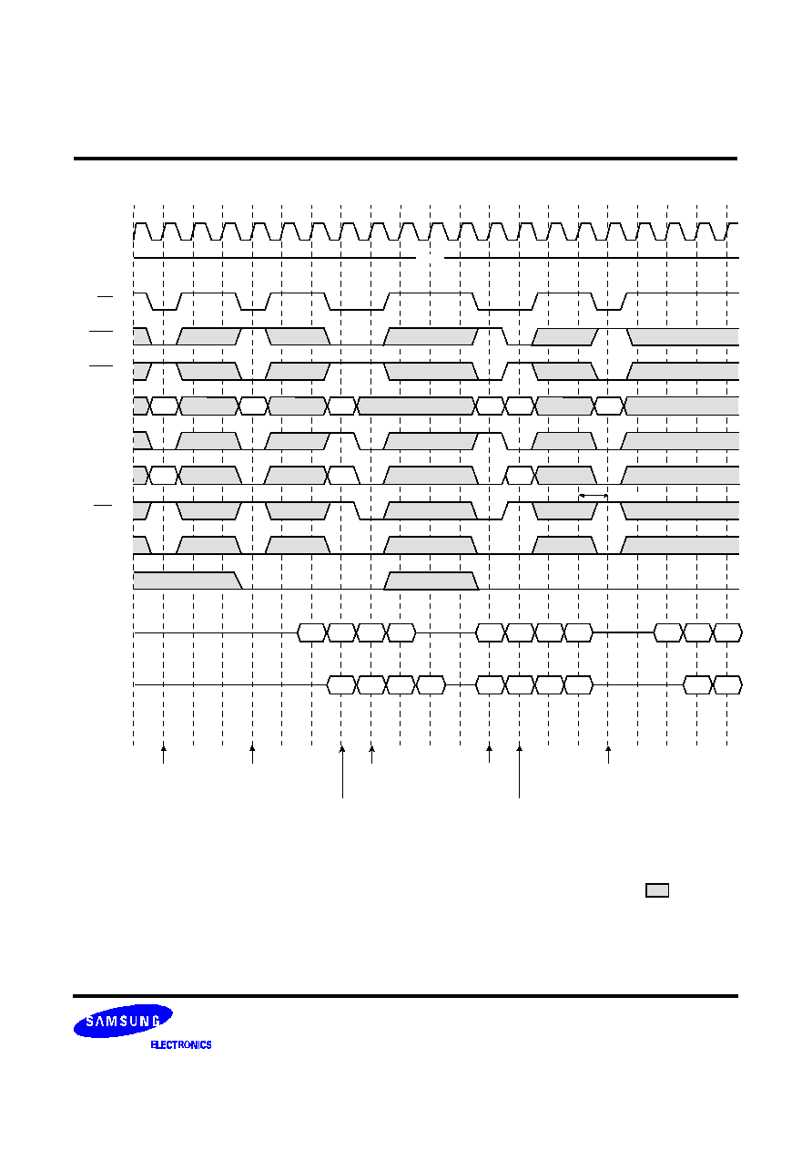
K4G323222M
CMOS SGRAM
Rev. 1.1 (Feb. 2000)
0
1
2
3
4
5
6
7
8
9
10
11
12
13
14
15
16
17
18
19
Read & Write Cycle at Different Bank @Burst Length=4
HIGH
Row Active
(A-Bank)
Write
(B-Bank)
Row Active
(A-Bank)
Read
(A-Bank)
*Note 1
t
CDL
Row Active
(B-Bank)
Precharge
(A-Bank)
Read
(A-Bank)
BA
A
8
/AP
ADDR
CAS
RAS
CS
CKE
CLOCK
WE
DQM
QAa0
QAa1
QAa2 QAa3
QAa0 QAa1
QAa2 QAa3
DBb0
DBb1
DBb2 DBb3
DBb0
DBb1
DBb2 DBb3
QAc0
QAc1 QAc2
QAc0
QAc1
RAa
CAa
RBb
CBb
RAc
CAc
RAc
RAa
RBb
DSF
: Don
t care
*Note : 1.
t
CDL
should be met to complete write.
(CL=2)
(CL=3)
DQ
DQ
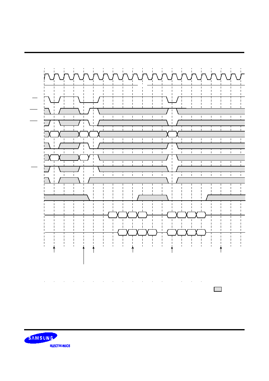
K4G323222M
CMOS SGRAM
Rev. 1.1 (Feb. 2000)
0
1
2
3
4
5
6
7
8
9
10
11
12
13
14
15
16
17
18
19
Read & Write Cycle with Auto Precharge I @Burst Length=4
HIGH
Row Active
(A-Bank)
1.
t
RCD
should be controlled to meet minimum
t
RAS
before internal precharge start.
(In the case of Burst Length=1 & 2, BRSW mode and Block write)
Row Active
(B-Bank)
Read with
Auto Precharge
(A-Bank)
Auto Precharge
Start Point
(B-Bank)
Auto Precharge
Start Point
(A-Bank)
Write with
Auto Precharge
(B-Bank)
ADDR
CAS
RAS
CS
CKE
CLOCK
WE
DQMi
RAa
RBb
CAa
RBb
CBb
DSF
*Note :
: Don
t care
(CL=2)
(CL=3)
DQ
DQ
RAa
QAa0
QAa1
QAa2 QAa3
QAa0 QAa1
QAa2 QAa3
DBb0
DBb1 DBb2 DBb3
DBb0
DBb1
DBb2 DBb3
BA
A
8
/AP
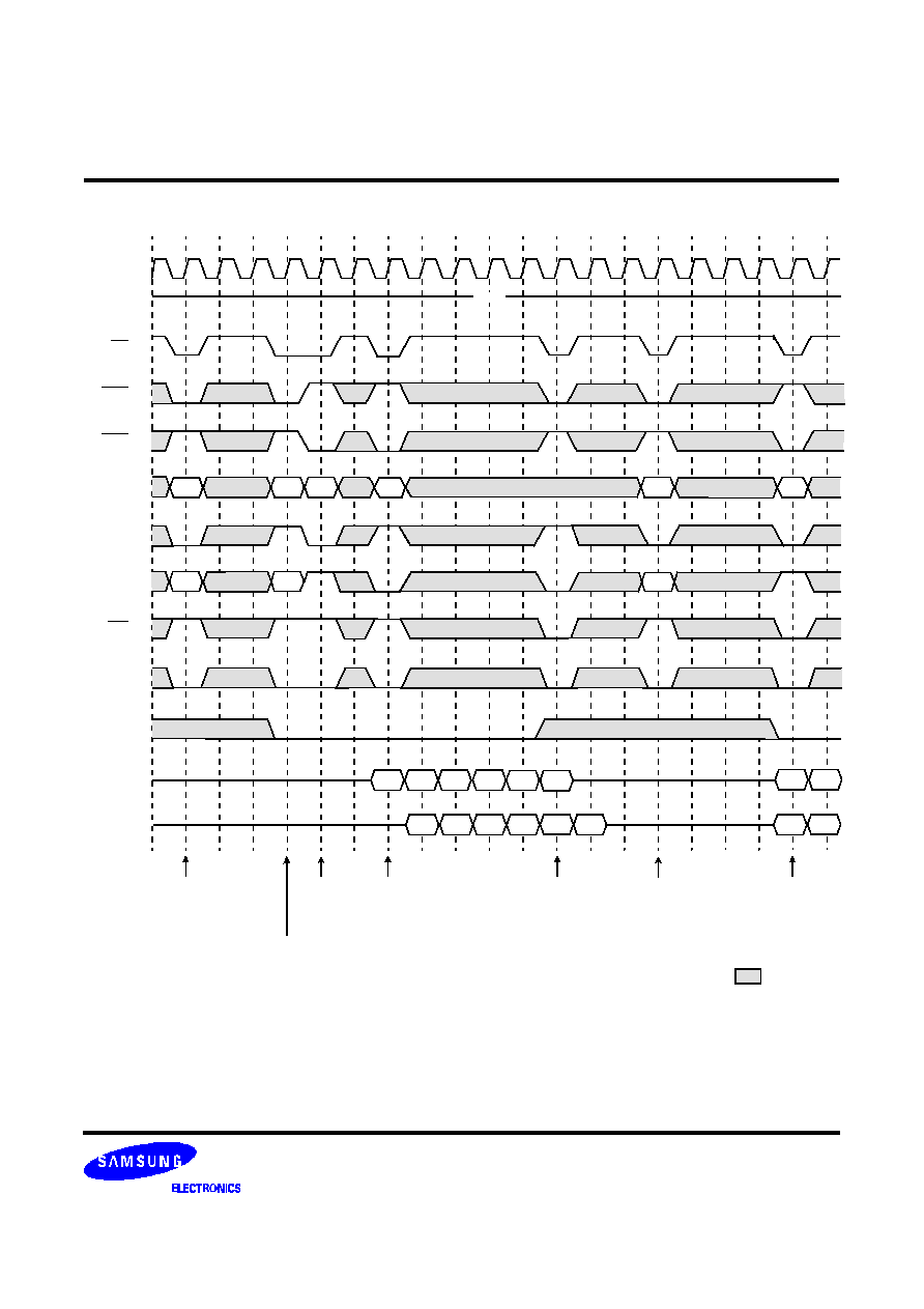
K4G323222M
CMOS SGRAM
Rev. 1.1 (Feb. 2000)
Read without Auto
precharge(B-Bank)
Auto Precharge
Start Point
(A-Bank)
Read & Write Cycle with Auto Precharge II @Burst Length=4
HIGH
Row Active
(A-Bank)
: Don
t care
*Note:
1. When Read(Write) command with auto precharge is issued at A-Bank after A and B Bank activation.
- if Read(Write) command without auto precharge is issued at B-Bank before A Bank auto precharge starts, A Bank
auto precharge will start at B Bank read command input point .
- any command can not be issued at A Bank during tRP after A Bank auto precharge starts.
Row Active
(B-Bank)
Read with
Auto Pre
charge
(A-Bank)
Write with
Auto Precharge
(A-Bank)
Row Active
(A-Bank)
ADDR
CAS
RAS
CS
CKE
CLOCK
WE
DQM
Qa0
Qa1
Qb0
Qb1
Qa0
Qa1
Qb0
Qb1
Ra
Rb
Ca
Ra
Rb
Ra
Cb
Qb2
Qb3
Precharge
(B-Bank)
Ca
Ra
Da0
Da1
Da0
Da1
Qb2
Qb3
0
1
2
3
4
5
6
7
8
9
10
11
12
13
14
15
16
17
18
19
(CL=2)
(CL=3)
DQ
DQ
DSF
*Note 1
BA
A
8
/AP
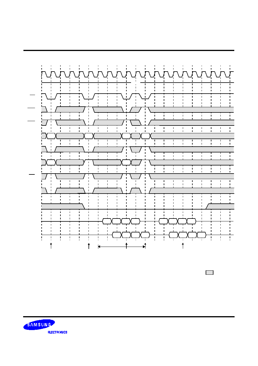
K4G323222M
CMOS SGRAM
Rev. 1.1 (Feb. 2000)
Read & Write Cycle with Auto Precharge III @Burst Length=4
HIGH
Row Active
(A-Bank)
: Don
t care
*Note :
1. Any command to A-bank is not allowed in this period.
tRP is determined from at auto precharge start point
Read with
Auto Precharge
(A-Bank)
Auto Precharge
Start Point
(A-Bank)
Row Active
(B-Bank)
Read with
Auto Precharge
(B-Bank)
ADDR
CAS
RAS
CS
CKE
CLOCK
WE
Qa0
Qa1
Qa2
Qa3
Qa0
Qa1
Qa2
Qa3
Qb0
Qb1
Qb2
Qb3
Qb0
Qb1
Qb2
Qb3
Ra
Ca
Ra
Cb
Rb
Rb
Auto Precharge
Start Point
(B-Bank)
0
1
2
3
4
5
6
7
8
9
10
11
12
13
14
15
16
17
18
19
DQM
DSF
(CL=2)
(CL=3)
DQ
DQ
*Note 1
BA
A
8
/AP
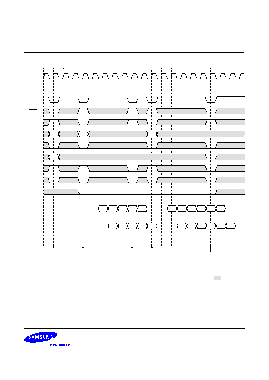
K4G323222M
CMOS SGRAM
Rev. 1.1 (Feb. 2000)
0
1
2
3
4
5
6
7
8
9
10
11
12
13
14
15
16
17
18
19
Read Interrupted by Precharge Command & Read Burst Stop Cycle (@Full page Only)
HIGH
Row Active
(A-Bank)
1. At full page mode, burst is wrap-around at the end of burst. So auto precharge is impossible.
2. About the valid DQ
s after burst stop, it is same as the case of RAS interrupt.
Both cases are illustrated above timing diagram. See the label 1, 2 on them.
But at burst write, Burst stop and RAS interrupt should be compared carefully.
Refer the timing diagram of "Full page write burst stop cycle".
*Note 1
Precharge
(A-Bank)
Read
(A-Bank)
Read
(A-Bank)
1
2
1
2
BA
A
8
/AP
ADDR
CAS
RAS
CS
CKE
CLOCK
WE
DQM
QAa0 QAa1 QAa2 QAa3 QAa4
QAa0 QAa1 QAa2 QAa3 QAa4
QAb0 QAb1 QAb2 QAb3 QAb4 QAb5
QAb0 QAb1 QAb2 QAb3 QAb4 QAb5
RAa
CAa
CAb
RAa
*Note 1
DSF
*Note 2
: Don
t care
Burst Stop
*Note :
(CL=2)
(CL=3)
DQ
DQ
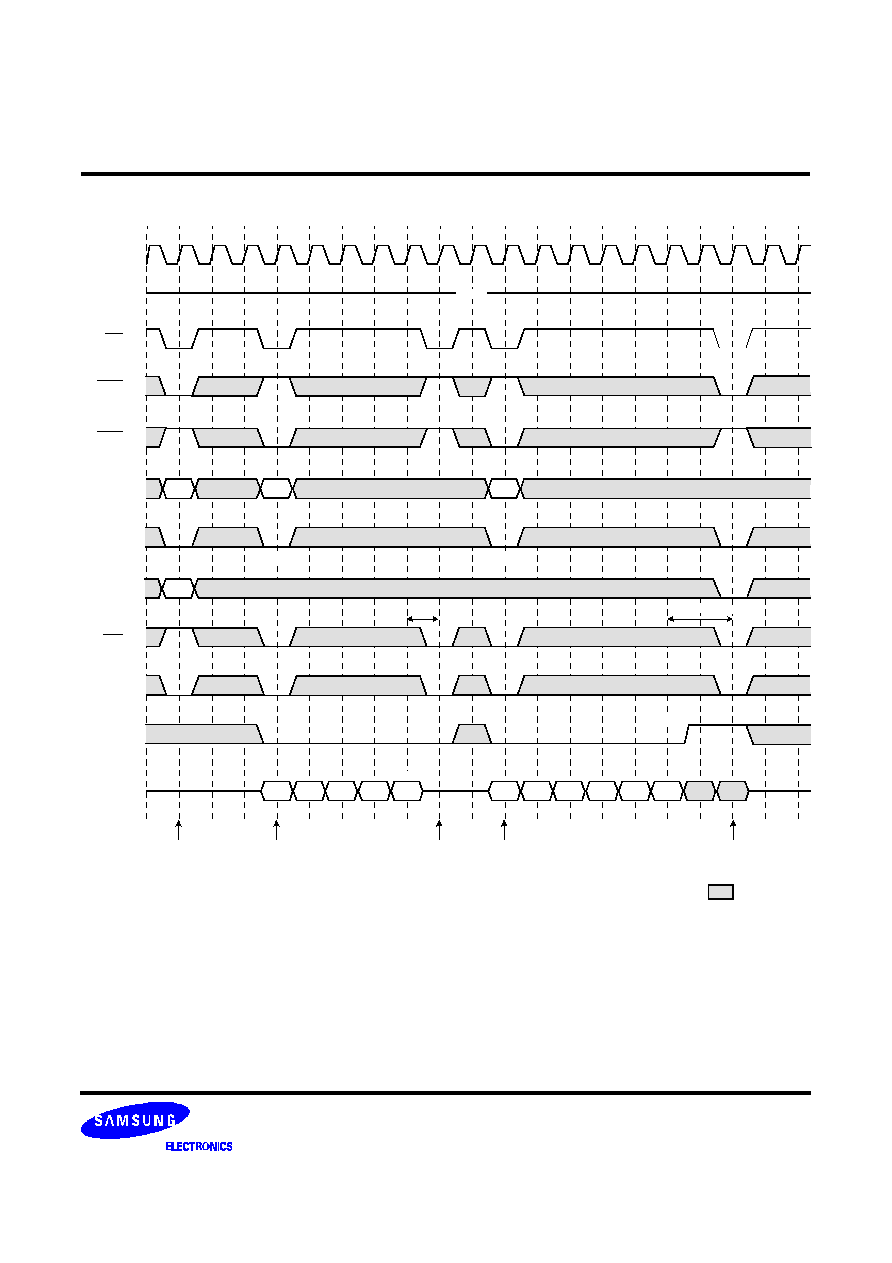
K4G323222M
CMOS SGRAM
Rev. 1.1 (Feb. 2000)
0
1
2
3
4
5
6
7
8
9
10
11
12
13
14
15
16
17
18
19
Write Interrupted by Precharge Command & Write Burst Stop Cycle (@ Full page Only)
Row Active
(A-Bank)
Write
(A-Bank)
Precharge
(A-Bank)
Write
(A-Bank)
*Note 3
tBDL
1. At full page mode, burst is wrap-around at the end of burst. So auto precharge is impossible.
2. Data-in at the cycle of burst stop command cannot be written into the corresponding memory cell.
It is defined by AC parameter of
t
BDL
(=1CLK).
3. Data-in at the cycle of interrupted by precharge cannot be written into the corresponding memory cell.
It is defined by AC parameter of
t
RDL
(=2CLK).
DQM at write interrupted by precharge command is needed to ensure
t
RDL
of 2CLK.
DQM should mask invalid input data on precharge command cycle when asserting precharge before end of burst.
Input data after Row precharge cycle will be masked internally.
4. Burst stop is valid only at full page burst length.
5. For -55/60/70/80, tRDL=1CLK product can be supported within restricted amounts and it will be distinguished by bucket code
"NV". From the next generation, tRDL will be only 2CLK for every clock frequency.
HIGH
t
RDL
BA
DQ
ADDR
CAS
RAS
CS
CKE
CLOCK
WE
DQM
A
8
/AP
DAa0
DAa1
DAa2
DAa3 DAa4
DAb0
DAb1
DAb2
DAb3 DAb4
DAb5
RAa
CAa
CAb
RAa
DSF
*Note 1
*Note 1
*Note 2
Burst Stop
*Note :
: Don
t care
*Note 5
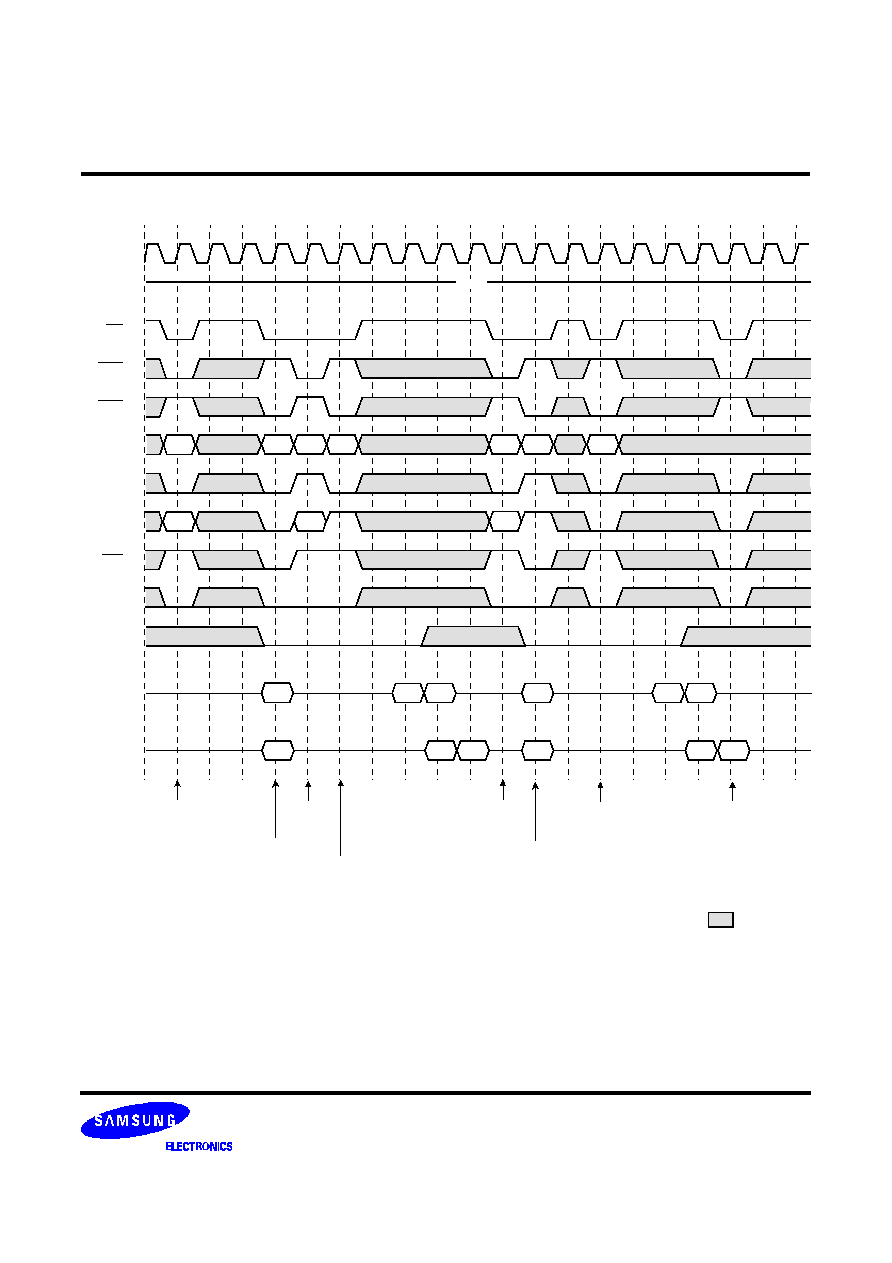
K4G323222M
CMOS SGRAM
Rev. 1.1 (Feb. 2000)
0
1
2
3
4
5
6
7
8
9
10
11
12
13
14
15
16
17
18
19
*Note 1
Burst Read Single bit Write Cycle @Burst Length=2, BRSW
HIGH
Row Active
(A-Bank)
Row Active
(A-Bank)
Write with
Auto Precharge
(B-Bank)
1. BRSW mode is enabled by setting A
9
"High" at MRS (Mode Register Set).
At the BRSW Mode, the burst length at write is fixed to "1" regardless of programed burst length.
2. When BRSW write command with auto precharge is executed, keep it in mind that
t
RAS
should not be violated.
Auto precharge is executed at the burst-end cycle, so in the case of BRSW write command,
the next cycle starts the precharge.
3. WPB function is also possible at BRSW mode.
Write
(A-Bank)
Row Active
(B-Bank)
Read
(A-Bank)
Read with
Auto Precharge
(A-Bank)
Precharge
(A-Bank)
*Note 2
BA
A
8
/AP
ADDR
CAS
RAS
CS
CKE
CLOCK
WE
DQMi
DAa0
DAa0
QAb0
QAb1
QAb0
QAb1
DBc0
DBc0
QAd0
QAd1
QAd0
QAd1
RAa
CAa
RBb
CAb
RAc
CBc
CAd
RAc
RAa
RBb
DSF
*Note :
: Don
t care
(CL=2)
(CL=3)
DQ
DQ
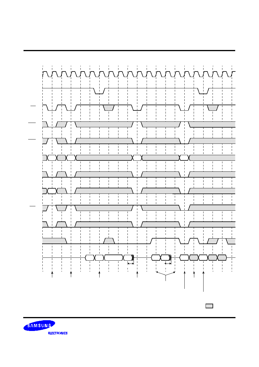
K4G323222M
CMOS SGRAM
Rev. 1.1 (Feb. 2000)
0
1
2
3
4
5
6
7
8
9
10
11
12
13
14
15
16
17
18
19
Clock suspension & DQM operation cycle @CAS Latency=2, Burst Length=4
Clock
Suspension
Clock
Suspension
*Note 1
t
SH
Z
t
SH
Z
Write
DQM
BA
DQ
ADDR
CAS
RAS
CS
CKE
CLOCK
WE
DQM
A
8
/AP
Ra
Ca
Cb
Cc
Dc2
Dc0
Qb1
Qb0
Qa3
Qa2
Qa1
Qa0
Ra
DSF
: Don
t care
*Note : 1. DQM needed to prevent bus contention.
Row Active
Read
Read
Read DQM
Write
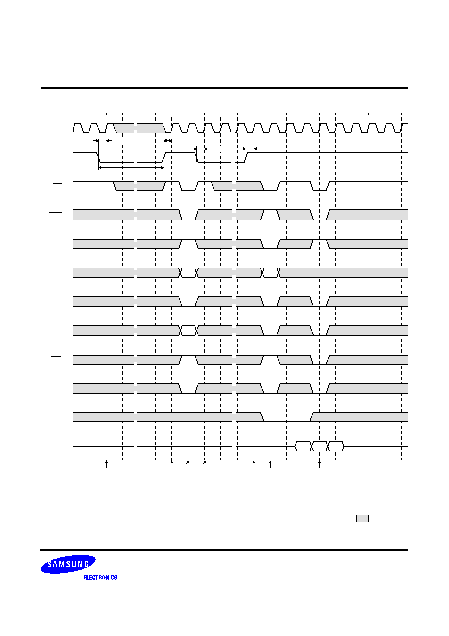
K4G323222M
CMOS SGRAM
Rev. 1.1 (Feb. 2000)
0
1
2
3
4
5
6
7
8
9
10
11
12
13
14
15
16
17
18
19
Active/Precharge Power Down Mode @CAS Lantency=2, Burst Length=4
Precharge
Power-down
Entry
1. All banks should be in idle state prior to entering precharge power down mode.
2. CKE should be set high at least "1CLK +
t
SS
" prior to Row active command.
3. Cannot violate minimum refresh specification. (32ms)
*Note 1
t
SS
*Note 2
BA
DQ
ADDR
CAS
RAS
CS
CKE
CLOCK
WE
DQM
A
8
/AP
t
SS
t
SS
Ra
Ca
Ra
Qa0
Qa1
Qa2
Active
Power-down
Entry
Active
Power-down
Exit
*Note 3
DSF
t
SS
Precharge
Power-down
Exit
Row Active
Read
Precharge
: Don
t care
*Note :
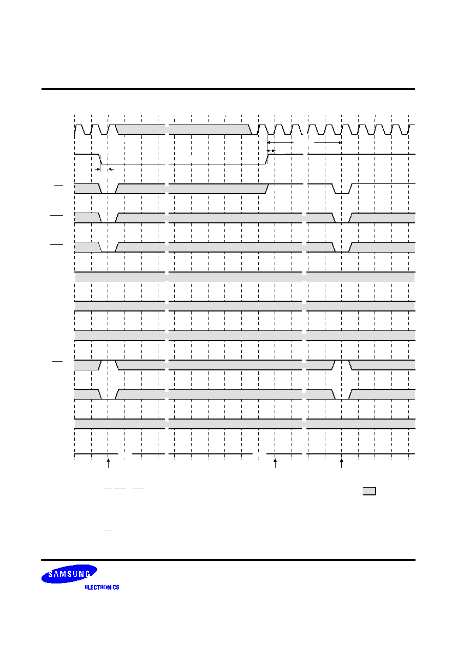
K4G323222M
CMOS SGRAM
Rev. 1.1 (Feb. 2000)
0
1
2
3
4
5
6
7
8
9
10
11
12
13
14
15
16
17
18
19
Self Refresh Entry & Exit Cycle
TO ENTER SELF REFRESH MODE
1. CS, RAS & CAS with CKE should be low at the same clock cycle.
2. After 1 clock cycle, all the inputs including the system clock can be don
t care except for CKE.
3. The device remains in self refresh mode as long as CKE stays
"Low".
cf.) Once the device enters self refresh mode, minimum
t
RAS
is required before exit from self refresh.
TO EXIT SELF REFRESH MODE
4. System clock restart and be stable before returning CKE high.
5. CS starts from high.
6. Minimum
t
RC
is required after CKE going high to complete self refresh exit.
7. 2K cycle of burst auto refresh is required before self refresh entry and after self refresh exit
if the system uses burst refresh.
*Note 1
*Note 7
Hi-Z
Hi-Z
t
SS
*Note 2
*Note 3
*Note 4
t
RC
min.
*Note 6
*Note 5
BA
DQ
ADDR
CAS
RAS
CS
CKE
CLOCK
WE
DQM
A
8
/AP
DSF
*Note 7
t
SS
Self Refresh Entry
Self Refresh Exit
Auto Refresh
: Don
t care
*Note :
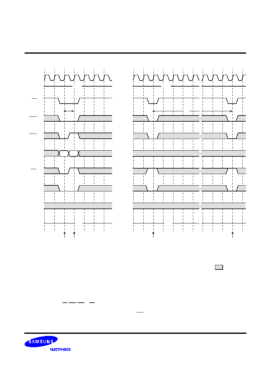
K4G323222M
CMOS SGRAM
Rev. 1.1 (Feb. 2000)
0
1
2
3
4
5
6
0
1
2
3
4
5
6
7
8
9
10
Mode Register Set Cycle
HIGH
1. CS, RAS, CAS, & WE activation and DSF of low at the same clock cycle with address key will set internal
mode register.
2. Minimum 1 clock cycles should be met before new RAS activation.
3. Please refer to Mode Register Set table.
New
Command
Hi-Z
Hi-Z
t
RC
HIGH
Auto Refresh Cycle
DQ
ADDR
CAS
RAS
CS
CKE
CLOCK
WE
DQM
Key
Ra
*Note 3
*Note 1
*Note 2
DSF
MRS
Auto Refresh
New Command
: Don
t care
* Both banks precharge should be completed before Mode Register Set cycle and auto refresh cycle.
MODE REGISTER SET CYCLE
*Note :
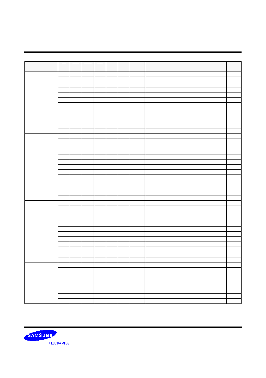
K4G323222M
CMOS SGRAM
Rev. 1.1 (Feb. 2000)
FUNCTION TRUTH TABLE(TABLE 1)
Current
State
CS
RAS
CAS
WE
DSF
BA
ADDR
ACTION
NOTE
IDLE
H
X
X
X
X
X
X
NOP
L
H
H
H
X
X
X
NOP
L
H
H
L
X
X
X
ILLEGAL
2
L
H
L
X
X
BA
CA
ILLEGAL
2
L
L
H
H
L
BA
RA
Row Active ; Latch Row Address ; Non-IO Mask
L
L
H
H
H
BA
RA
Row Active ; Latch Row Address ; IO Mask
L
L
H
L
L
BA
PA
NOP
4
L
L
H
L
H
X
X
ILLEGAL
L
L
L
H
L
X
X
Auto Refresh or Self Refresh
5
L
L
L
H
H
X
X
ILLEGAL
L
L
L
L
L
OP Code
Mode Register Access
5
L
L
L
L
H
OP Code
Special Mode Register Access
6
Row
Active
H
X
X
X
X
X
X
NOP
L
H
H
H
X
X
X
NOP
L
H
H
L
X
X
X
ILLEGAL
2
L
H
L
H
L
BA
CA,AP
Begin Read ; Latch CA ; Determine AP
L
H
L
H
H
X
X
ILLEGAL
L
H
L
L
L
BA
CA,AP
Begin Write ;Latch CA ; Determine AP
L
H
L
L
H
BA
CA,AP
Block Write ;Latch CA ; Determine AP
L
L
H
H
X
BA
RA
ILLEGAL
2
L
L
H
L
L
BA
PA
Precharge
L
L
H
L
H
X
X
ILLEGAL
L
L
L
H
X
X
X
ILLEGAL
L
L
L
L
L
X
X
ILLEGAL
L
L
L
L
H
OP Code
Special Mode Register Access
6
Read
H
X
X
X
X
X
X
NOP(Continue Burst to End --> Row Active)
L
H
H
H
X
X
X
NOP(Continue Burst to End --> Row Active)
L
H
H
L
L
X
X
Term burst --> Row active
L
H
H
L
H
X
X
ILLEGAL
L
H
L
H
L
BA
CA,AP
Term burst ; Begin Read ; Latch CA ; Determine AP
3
L
H
L
H
H
X
X
ILLEGAL
L
H
L
L
L
BA
CA,AP
Term burst ; Begin Write ; Latch CA ; Determine AP
3
L
H
L
L
H
BA
CA.AP
Term burst ; Block Write ; Latch CA ; Determine AP
3
L
L
H
H
X
BA
RA
ILLEGAL
2
L
L
H
L
L
BA
PA
Term Burst ; Precharge timing for Reads
3
L
L
H
L
H
X
X
ILLEGAL
L
L
L
X
X
X
X
ILLEGAL
Write
H
X
X
X
X
X
X
NOP(Continue Burst to End --> Row Active)
L
H
H
H
X
X
X
NOP(Continue Burst to End --> Row Active)
L
H
H
L
L
X
X
Term burst --> Row active
L
H
H
L
H
X
X
ILLEGAL
L
H
L
H
L
BA
CA,AP
Term burst ; Begin Read ; Latch CA ; Determine AP
3
L
H
L
H
H
X
X
ILLEGAL
L
H
L
L
L
BA
CA,AP
Term burst ; Begin Write ; Latch CA ; Determine AP
3
L
H
L
L
H
BA
CA,AP
Term burst ; Block Write ; Latch CA ; Determine AP
3
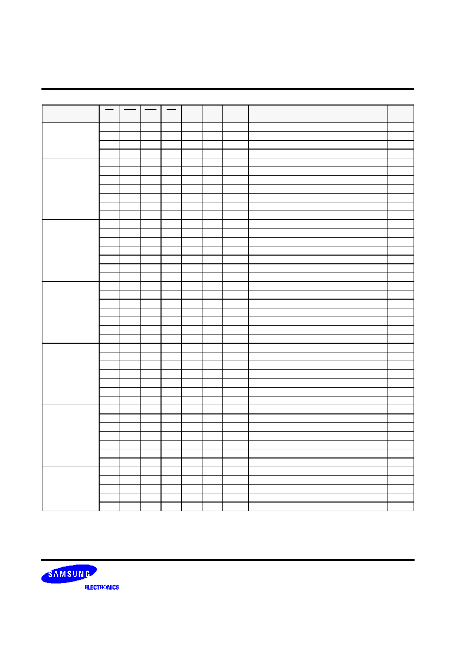
K4G323222M
CMOS SGRAM
Rev. 1.1 (Feb. 2000)
FUNCTION TRUTH TABLE(TABLE 1, Continued)
Current
State
CS
RAS
CAS
WE
DSF
BA
ADDR
ACTION
NOTE
Write
L
L
H
H
X
BA
RA
ILLEGAL
2
L
L
H
L
L
BA
PA
Term Burst : Precharge timing for Writes
3
L
L
H
L
H
X
X
ILLEGAL
L
L
L
X
X
X
X
ILLEGAL
Read with
Auto
Precharge
H
X
X
X
X
X
X
NOP(Continue Burst to End --> Precharge)
L
H
H
H
X
X
X
NOP(Continue Burst to End --> Precharge)
L
H
H
L
X
X
X
ILLEGAL
L
H
L
H
X
BA
CA,AP
ILLEGAL
2
L
H
L
L
X
BA
CA,AP
ILLEGAL
2
L
L
H
X
X
BA
RA,PA
ILLEGAL
L
L
L
X
X
X
X
ILLEGAL
2
Write with
Auto
Precharge
H
X
X
X
X
X
X
NOP(Continue Burst to End --> Precharge)
L
H
H
H
X
X
X
NOP(Continue Burst to End --> Precharge)
L
H
H
L
X
X
X
ILLEGAL
L
H
L
H
X
BA
CA,AP
ILLEGAL
2
L
H
L
L
X
BA
CA,AP
ILLEGAL
2
L
L
H
X
X
BA
RA,PA
ILLEGAL
L
L
L
X
X
X
X
ILLEGAL
2
Precharging
H
X
X
X
X
X
X
NOP --> Idle after
t
RP
L
H
H
H
X
X
X
NOP --> Idle after
t
RP
L
H
H
L
X
X
X
ILLEGAL
L
H
L
X
X
BA
CA,AP
ILLEGAL
2
L
L
H
H
X
BA
RA
ILLEGAL
2
L
L
H
L
X
BA
PA
NOP --> Idle after
t
RP
2
L
L
L
X
X
X
X
ILLEGAL
4
Block
Write
Recovering
H
X
X
X
X
X
X
NOP --> Row Active after
t
BWC
L
H
H
H
X
X
X
NOP --> Row Active after
t
BWC
L
H
H
L
X
X
X
ILLEGAL
L
H
L
X
X
BA
CA,AP
ILLEGAL
2
L
L
H
H
X
BA
RA
ILLEGAL
2
L
L
H
L
X
BA
PA
Term Block Write : Precharge timing for Block Write
2
L
L
L
X
X
X
X
ILLEGAL
2
Row
Activating
H
X
X
X
X
X
X
NOP --> Row Active after
t
RCD
L
H
H
H
X
X
X
NOP --> Row Active after
t
RCD
L
H
H
L
X
X
X
ILLEGAL
L
H
L
X
X
BA
CA,AP
ILLEGAL
2
L
L
H
H
X
BA
RA
ILLEGAL
2
L
L
H
L
X
BA
PA
ILLEGAL
2
L
L
L
X
X
X
X
ILLEGAL
2
Refreshing
H
X
X
X
X
X
X
NOP --> Idle after
t
RC
L
H
H
X
X
X
X
NOP --> Idle after
t
RC
L
H
L
X
X
X
X
ILLEGAL
L
L
H
X
X
X
X
ILLEGAL
L
L
L
X
X
X
X
ILLEGAL
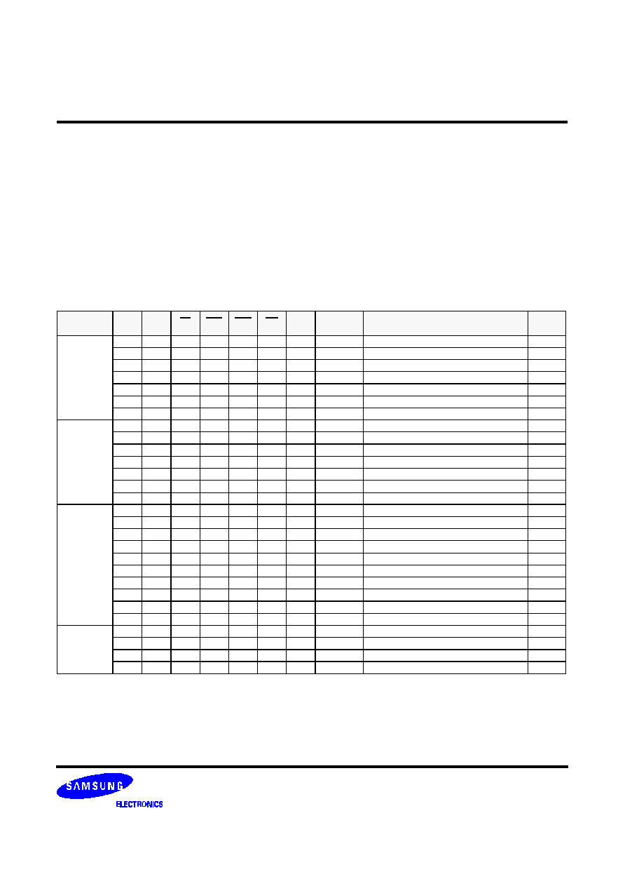
K4G323222M
CMOS SGRAM
Rev. 1.1 (Feb. 2000)
1. All entries assume that CKE was active(High) during the preceding clock cycle and the current clock cycle.
2. Illegal to bank in specified state ; Function may be legal in the bank indicated by BA, depending on the state of that bank.
3. Must satisfy bus contention, bus turn around, and/or write recovery requirements.
4. NOP to bank precharging or in idle state. May precharge bank indicated by BA(and PA).
5. Illegal if any banks is not idle.
6. Legal only if all banks are in idle or row active state.
RA = Row Address(A
0
~A
10
)
NOP = No Operation Command
BA = Bank Address
CA = Column Address(A
0
~A
7
)
PA = Precharge All(A
8
)
AP = Auto Precharge(A
8
)
FUNCTION TRUTH TABLE for CKE(TABLE 2)
Current
State
CKE
n-1
CKE
n
CS
RAS
CAS
WE
DSF
ADDR
ACTION
NOTE
Self
Refresh
H
X
X
X
X
X
X
X
INVALID
L
H
H
X
X
X
X
X
Exit Self Refresh --> ABI after
t
RC
7
L
H
L
H
H
H
X
X
Exit Self Refresh --> ABI after
t
RC
7
L
H
L
H
H
L
X
X
ILLEGAL
L
H
L
H
L
X
X
X
ILLEGAL
L
H
L
L
X
X
X
X
ILLEGAL
L
L
X
X
X
X
X
X
NOP(Maintain Self Refresh)
Both
Bank
Precharge
Power
Down
H
X
X
X
X
X
X
X
INVALID
L
H
H
X
X
X
X
X
Exit Power Down --> ABI
8
L
H
L
H
H
H
X
X
Exit Power Down --> ABI
8
L
H
L
H
H
L
X
X
ILLEGAL
L
H
L
H
L
X
X
X
ILLEGAL
L
H
L
L
X
X
X
X
ILLEGAL
L
L
X
X
X
X
X
X
NOP(Maintain Power Down Mode)
All
Banks
Idle
H
H
X
X
X
X
X
X
Refer to Table 1
H
L
H
X
X
X
X
X
Enter Power Down
9
H
L
L
H
H
H
X
X
Enter Power Down
9
H
L
L
H
H
L
X
X
ILLEGAL
H
L
L
H
L
X
X
X
ILLEGAL
H
L
L
L
H
H
L
RA
Row (& Bank) Active
H
L
L
L
L
H
L
X
Enter Self Refresh
9
H
L
L
L
L
L
L
OP Code
Mode Register Access
H
L
L
L
L
L
H
OP Code
Special Mode Register Access
L
L
X
X
X
X
X
X
NOP
Any State
other than
Listed
Above
H
H
X
X
X
X
X
X
Refer to Operations in Table 1
H
L
X
X
X
X
X
X
Begin Clock Suspend next cycle
10
L
H
X
X
X
X
X
X
Exit Clock Suspend next cycle
10
L
L
X
X
X
X
X
X
Maintain clock Suspend
7. After CKE
s low to high transition to exist self refresh mode. And a time of
t
RC
(min) has to be elapse after CKE
s low to high
transition to issue a new command.
8. CKE low to high transition is asynchronous as if restarts internal clock.
A minimum setup time "
t
SS
+ one clock" must be satisfied before any command other than exit.
9. Power-down and self refresh can be entered only from the all banks idle state.
10. Must be a legal command.
FUNCTION TRUTH TABLE (TABLE 1, Continued)
ABBREVIATIONS
*Note :
ABBREVIATIONS : ABI = All Banks Idle
*Note :
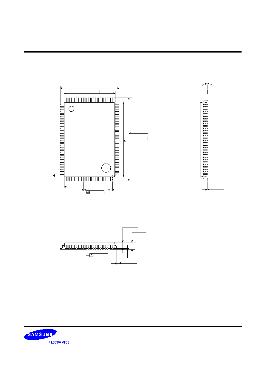
K4G323222M
CMOS SGRAM
Rev. 1.1 (Feb. 2000)
0.825
0
.
5
7
5
0.65
0.13 MAX
PACKAGE DIMENSIONS (TQFP)
Dimensions in Millimeters
0.10 MAX
0 ~ 7
∞
17.20
±
0.20
14.00
±
0.10
23.20
±
0.20
1.00
±
0.10
1.20 MAX *
0.05 MIN
0.80
±
0.20
#1
0.09~0.20
#100
0.30
±
0.08
20.00
±
0.10
* All Package Dimensions of PQFP & TQFP are same except Height.
- PQFP (Height = 3.0mmMAX)
- TQFP (Height = 1.2mmMAX)