Rev. 1.3 June. 2005
DDR SDRAM
DDR SDRAM 512Mb B-die (x8)
* Samsung Electronics reserves the right to change products or specification without notice.
INFORMATION IN THIS DOCUMENT IS PROVIDED IN RELATION TO SAMSUNG PRODUCTS,
AND IS SUBJECT TO CHANGE WITHOUT NOTICE.
NOTHING IN THIS DOCUMENT SHALL BE CONSTRUED AS GRANTING ANY LICENSE,
EXPRESS OR IMPLIED, BY ESTOPPEL OR OTHERWISE,
TO ANY INTELLECTUAL PROPERTY RIGHTS IN SAMSUNG PRODUCTS OR TECHNOLOGY. ALL
INFORMATION IN THIS DOCUMENT IS PROVIDED
ON AS "AS IS" BASIS WITHOUT GUARANTEE OR WARRANTY OF ANY KIND.
1. For updates or additional information about Samsung products, contact your nearest Samsung office.
2. Samsung products are not intended for use in life support, critical care, medical, safety equipment, or similar
applications where Product failure could result in loss of life or personal or physical harm, or any military or
defense application, or any governmental procurement to which special terms or provisions may apply.
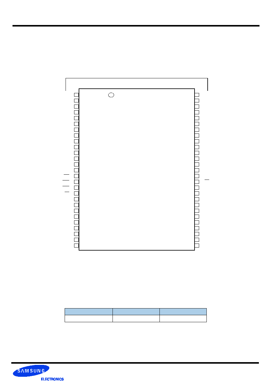
512Mb B-die DDR SDRAM Specification
54 sTSOP-II (400mil x 441mil)

Rev. 1.3 June. 2005
DDR SDRAM
DDR SDRAM 512Mb B-die (x8)
Table of Contents
1.0 Key Features ...............................................................................................................................4
2.0 Ordering Information...................................................................................................................4
3.0 Operating Frequencies................................................................................................................4
4.0 Pin Description ............................................................................................................................5
5.0 Package Physical Dimension .....................................................................................................6
6.0 Block Diagram (16Mbit x8 I/O x4 Banks) ...................................................................................7
7.0 Input/Output Function Description ............................................................................................8
8.0 Command Truth Table.................................................................................................................9
9.0 General Description...................................................................................................................10
10.0 Absolute Maximum Rating .....................................................................................................10
11.0 DC Operating Conditions ........................................................................................................10
12.0 DDR SDRAM Spec Items & Test Conditions .........................................................................11
13.0 Input/Output Capacitance ......................................................................................................11
14.0 Detailed test condition for DDR SDRAM IDD1 & IDD7A ......................................................12
15.0 DDR SDRAM IDD spec table ..................................................................................................13
16.0 AC Operating Conditions .......................................................................................................14
17.0 AC Overshoot/Undershoot specification for Address and Control Pins............................14
18.0 Overshoot/Undershoot specification for Data, Strobe and Mask Pins...............................15
19.0 AC Timming Parameters & Specifications ...........................................................................16
20.0 System Characteristics for DDR SDRAM ..............................................................................17
21.0 Component Notes ....................................................................................................................18
22.0 System Notes ...........................................................................................................................20
23.0 IBIS : I/V Characteristics for Input and Output Buffers ........................................................21
Rev. 1.3 June. 2005
DDR SDRAM
DDR SDRAM 512Mb B-die (x8)
� VDD : 2.5V � 0.2V, VDDQ : 2.5V � 0.2V for DDR266, 333
� VDD : 2.6V � 0.1V, VDDQ : 2.6V � 0.1V for DDR400
� Double-data-rate architecture; two data transfers per clock cycle
� Bidirectional data strobe [DQS] (x4,x8)
� Four banks operation
� Differential clock inputs(CK and CK)
� DLL aligns DQ and DQS transition with CK transition
� MRS cycle with address key programs
-. Read latency : DDR266(2, 2.5 Clock), DDR333(2.5 Clock), DDR400(3 Clock)
-. Burst length (2, 4, 8)
-. Burst type (sequential & interleave)
� All inputs except data & DM are sampled at the positive going edge of the system clock(CK)
� Data I/O transactions on both edges of data strobe
� Edge aligned data output, center aligned data input
� DM for write masking only (x4, x8)
� Auto & Self refresh
� 7.8us refresh interval(8K/64ms refresh)
� Maximum burst refresh cycle : 8
� 54pin sTSOP(II)-400
(Leaded & Pb-Free(RoHS compliant))
package
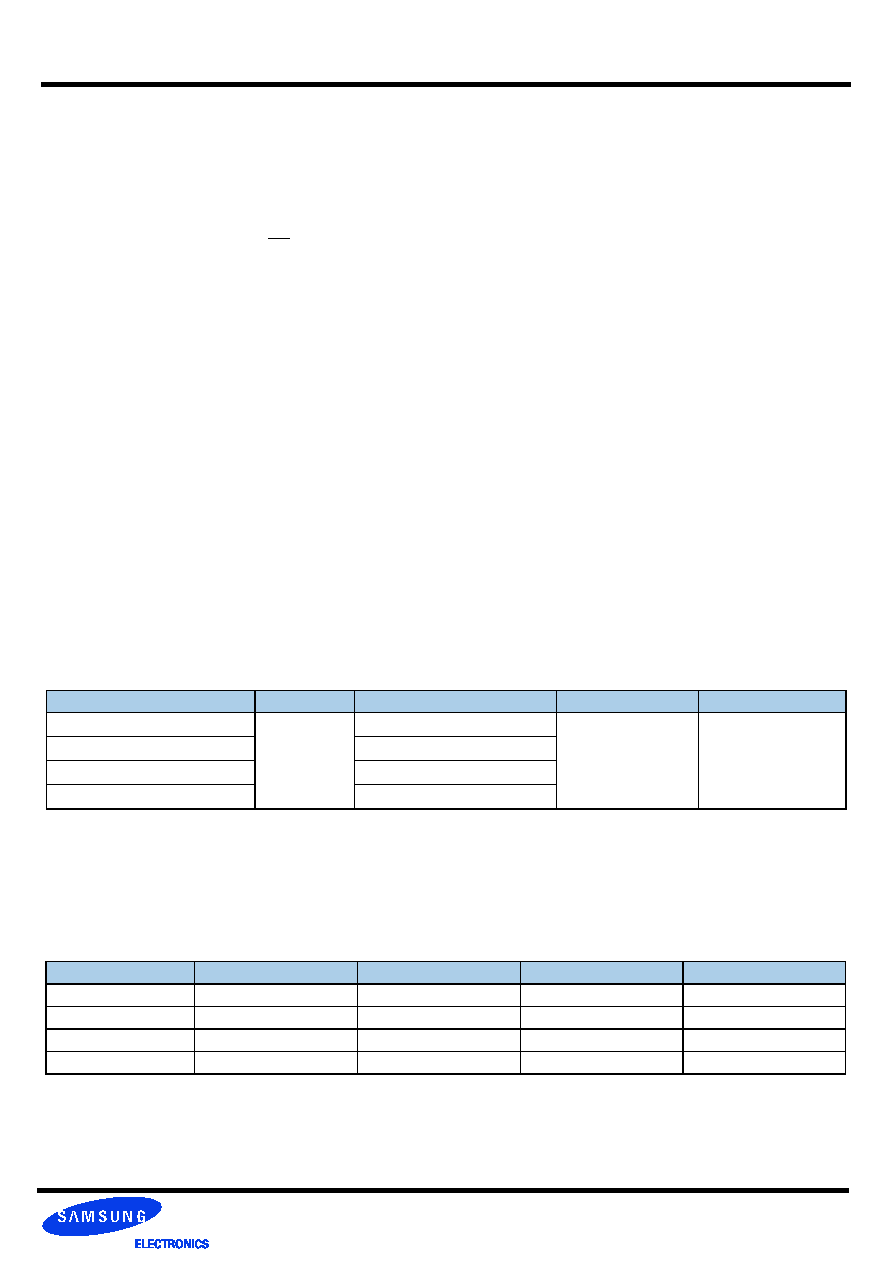
CC(DDR400@CL=3)
B3(DDR333@CL=2.5)
A2(DDR266@CL=2.0)
B0(DDR266@CL=2.5)
Speed @CL2
-
133MHz
133MHz
100MHz
Speed @CL2.5
166MHz
166MHz
133MHz
133MHz
Speed @CL3
200MHz
-
-
-
CL-tRCD-tRP
3-3-3
2.5-3-3
2-3-3
2.5-3-3
Note : Leaded and Lead-free(Pb-free) can be discriminated by PKG P/N (N : 54 sTSOP with Leaded, V : 54 sTSOP with Lead-free)
Part No.
Org.
Max Freq.
Interface
Package
K4H510838B-N(V)C/LCC
64M x 8
CC(DDR400@CL=3)
SSTL2
54pin sTSOP II
K4H510838B-N(V)C/LB3
B3(DDR333@CL=2.5)
K4H510838B-N(V)C/LA2
A2(DDR266@CL=2)
K4H510838B-N(V)C/LB0
B0(DDR266@CL=2.5)
1.0 Key Features
2.0 Ordering Information
3.0 Operating Frequencies