
- 1 -
REV. 0.0 Feb. 5. 2002
DDP 512Mb(x8) DDR SDRAM
DDR SDRAM Specification
Version 0.0
This is to advise Samsung customers that in accordance with certain terms of an agreement, Samsung is prohibited from selling any DRAM
products configured in "Multi-Die Plastic" format for use as components in general and scientific computers, such as mainframes, servers,
work stations or desk top personal computers (hereinafter "Prohibited Computer Use"). Applications such as mobile, including cell phones,
telecom, including televisions and display monitors, or non-desktop computer systems, including laptops, notebook computers, are,
however, permissible. "Multi-Die Plastic" is defined as two or more Dram die encapsulated within a single plastic leaded package.

- 2 -
REV. 0.0 Feb. 5. 2002
DDP 512Mb(x8) DDR SDRAM
Revision History
Version 0 (February, 2002)
- First version for internal review

- 3 -
REV. 0.0 Feb. 5. 2002
DDP 512Mb(x8) DDR SDRAM
General Information
Organization
166Mhz w/ CL=2.5
133Mhz w/ CL=2
133Mhz w/ CL=2.5
100Mhz w/ CL=2
64Mx8
K4H510838C-KCB3
K4H510838C-KCA2
K4H510838C-KCB0
K4H510838C-KCA0
T
: TSOP2 (400mil x 875mil)
K
: 400mi DDP TSOP2
B3
: 6ns@CL2.5
A0
: 10ns@CL2
A2
: 7.5ns@CL2
B0
: 7.5ns@CL2.5
C : (Commercial, Normal)
L : (Commercial, Low)
04
: x4
08
: x8
16
: x16
32
: x32
06
: stacked x4
64
: 64M 4K/64ms
28
: 128M 4K/64ms
56
: 256M 8K/64ms
51
: 512M 8K/64ms
1G
: 1G 16K/32ms
H
: DDR SDRAM
M
: 1st Generation
A
: 2nd Generation
B
: 3rd Generation
C
: 4th Generation
D
: 5th Generation
E
: 6th Generation
K 4 H XX XX X X X - X X
Memory
DRAM
Small Classification
Density and Refresh
Temperature & Power
Package
Organization
Version
Interface (VDD & VDDQ)
1. SAMSUNG Memory : K
2. DRAM : 4
3. Small Classification
4. Density & Refresh
5. Organization
8. Version
9. Package
10. Temperature & Power
11. Speed
3
: 4 Bank
6. Bank
1 2 3 4 5 6 7 8 9 10 11
XX
8
: SSTL-2(2.5V, 2.5V)
7. Interface (VDD & VDDQ)
Speed
Bank

- 4 -
REV. 0.0 Feb. 5. 2002
DDP 512Mb(x8) DDR SDRAM
�
Double-data-rate architecture; two data transfers per clock cycle
� Bidirectional data strobe(DQS)
� Four banks operation
� Differential clock inputs(CK and CK)
� DLL aligns DQ and DQS transition with CK transition
� MRS cycle with address key programs
-. Read latency 2, 2.5 (clock)
-. Burst length (2, 4, 8)
-. Burst type (sequential & interleave)
� All inputs except data & DM are sampled at the positive going edge of the system clock(CK)
� Data I/O transactions on both edges of data strobe
� Edge aligned data output, center aligned data input
� LDM,UDM/DM for write masking only
� Auto & Self refresh
� 7.8us refresh interval(8K/64ms refresh)
� Maximum burst refresh cycle : 8
� 54pin TSOP II package
Key Features
Operating Frequencies
*CL : Cas Latency
- B3(DDR333)
- A2(DDR266A)
- B0(DDR266B)
- A0(DDR200)
Speed @CL2
133MHz
133MHz
100MHz
100MHz
Speed @CL2.5
166MHz
133MHz
133MHz
-
DLL jitter
�0.7ns
�0.75ns
�0.75ns
�0.8ns
Functional Block Diagram
32Mx8
32Mx8
CK,CK,CAS
RAS,WE ,DM
CKE1,CS1
CKE0,CS0
I/O0 ~ I/O7,DQS
A0-A12,BA0,BA1
- 5 -
REV. 0.0 Feb. 5. 2002
DDP 512Mb(x8) DDR SDRAM
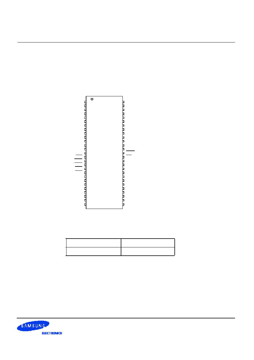
Package Pinout
DM is internally loaded to match DQ and DQS identically.
FIgure 1. 512Mb TSOP II package Pinout
Table 2. Column address configuration
Organization
Column Address
64Mx8
A0-A9
V
D D
DQ0
V
DDQ
DQ1
V
SSQ
DQ2
V
DDQ
DQ3
V
SSQ
N.C
V
DDQ
N.C
N.C
V
D D
WE
CAS
RAS
CS0
CS1
BA0
BA1
A10
A0
A1
A2
A3
V
D D
1
2
3
4
5
6
7
8
9
10
11
12
13
14
15
16
17
18
19
20
21
22
23
24
25
26
27
54
53
52
51
50
49
48
47
46
45
44
43
42
41
40
39
38
37
36
35
34
33
32
31
30
29
28
V
SS
DQ7
V
SSQ
DQ6
V
DDQ
DQ5
V
SSQ
DQ4
V
DDQ
V
SSQ
DQS
V
REF
V
SS
DQM
CK
CK
CKE0
CKE1
A12
A11
A9
A8
A7
A6
A5
A4
V
SS
54Pin TSOP (II)
(400mil x 875mil)
(0.8 mm Pin pitcH)