Rev. 0.3 June. 2005
DDR SDRAM
DDR SDRAM 512Mb D-die (x8, x16)
Preliminary
* Samsung Electronics reserves the right to change products or specification without notice.
INFORMATION IN THIS DOCUMENT IS PROVIDED IN RELATION TO SAMSUNG PRODUCTS,
AND IS SUBJECT TO CHANGE WITHOUT NOTICE.
NOTHING IN THIS DOCUMENT SHALL BE CONSTRUED AS GRANTING ANY LICENSE,
EXPRESS OR IMPLIED, BY ESTOPPEL OR OTHERWISE,
TO ANY INTELLECTUAL PROPERTY RIGHTS IN SAMSUNG PRODUCTS OR TECHNOLOGY. ALL
INFORMATION IN THIS DOCUMENT IS PROVIDED
ON AS "AS IS" BASIS WITHOUT GUARANTEE OR WARRANTY OF ANY KIND.
1. For updates or additional information about Samsung products, contact your nearest Samsung office.
2. Samsung products are not intended for use in life support, critical care, medical, safety equipment, or similar
applications where Product failure could result in loss of life or personal or physical harm, or any military or
defense application, or any governmental procurement to which special terms or provisions may apply.
512Mb D-die DDR SDRAM Specification
66 TSOP-II with Pb-Free
(RoHS compliant)

Rev. 0.3 June. 2005
DDR SDRAM
DDR SDRAM 512Mb D-die (x8, x16)
Preliminary
Table of Contents
1.0 Key Features ...............................................................................................................................4
2.0 Ordering Information...................................................................................................................4
3.0 Operating Frequencies................................................................................................................4
4.0 Pin Description ............................................................................................................................5
5.0 Package Physical Dimension .....................................................................................................6
6.0 Block Diagram (16Mbit x8 / 8Mbit x16 I/O x4 Banks) ................................................................7
7.0 Input/Output Function Description ............................................................................................8
8.0 Command Truth Table.................................................................................................................9
9.0 General Description...................................................................................................................10
10.0 Absolute Maximum Rating .....................................................................................................10
11.0 DC Operating Conditions ........................................................................................................10
12.0 DDR SDRAM Spec Items & Test Conditions .........................................................................11
13.0 Input/Output Capacitance ......................................................................................................11
14.0 Detailed test condition for DDR SDRAM IDD1 & IDD7A ......................................................12
15.0 DDR SDRAM IDD spec table ..................................................................................................13
16.0 AC Operating Conditions .......................................................................................................14
17.0 AC Overshoot/Undershoot specification for Address and Control Pins............................14
18.0 Overshoot/Undershoot specification for Data, Strobe and Mask Pins...............................15
19.0 AC Timming Parameters & Specifications ...........................................................................16
20.0 System Characteristics for DDR SDRAM ..............................................................................17
21.0 Component Notes ....................................................................................................................18
22.0 System Notes ...........................................................................................................................20
23.0 IBIS : I/V Characteristics for Input and Output Buffers ........................................................21
Rev. 0.3 June. 2005
DDR SDRAM
DDR SDRAM 512Mb D-die (x8, x16)
Preliminary
Revision History
Revision
Month
Year
History
0.0
December
2004
- First version for internal review
0.1
January
2005
- Preliminary spec release
0.2
April
2005
- Added notice
0.3
June
2005
- Changed Mater format.
Rev. 0.3 June. 2005
DDR SDRAM
DDR SDRAM 512Mb D-die (x8, x16)
Preliminary
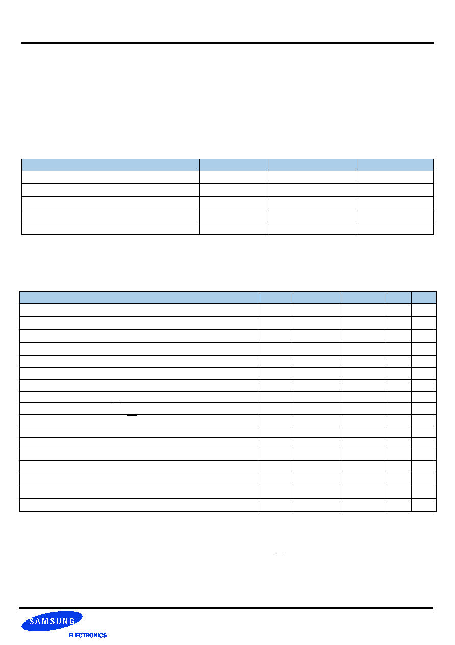
� VDD : 2.5V � 0.2V, VDDQ : 2.5V � 0.2V for DDR266, 333
� VDD : 2.6V � 0.1V, VDDQ : 2.6V � 0.1V for DDR400
� Double-data-rate architecture; two data transfers per clock cycle
� Bidirectional data strobe [DQS] (x4,x8) & [L(U)DQS] (x16)
� Four banks operation
� Differential clock inputs(CK and CK)
� DLL aligns DQ and DQS transition with CK transition
� MRS cycle with address key programs
-. Read latency : DDR266(2, 2.5 Clock), DDR333(2.5 Clock), DDR400(3 Clock)
-. Burst length (2, 4, 8)
-. Burst type (sequential & interleave)
� All inputs except data & DM are sampled at the positive going edge of the system clock(CK)
� Data I/O transactions on both edges of data strobe
� Edge aligned data output, center aligned data input
� LDM,UDM for write masking only (x16)
� DM for write masking only (x4, x8)
� Auto & Self refresh
� 7.8us refresh interval(8K/64ms refresh)
� Maximum burst refresh cycle : 8
� 66pin TSOP II
Pb-Free
package
�
RoHS compliant
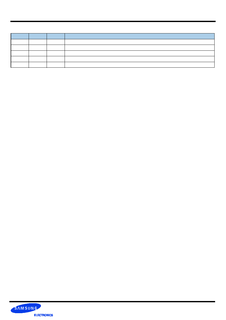
CC(DDR400@CL=3)
B3(DDR333@CL=2.5)
A2(DDR266@CL=2.0)
B0(DDR266@CL=2.5)
Speed @CL2
-
133MHz
133MHz
100MHz
Speed @CL2.5
166MHz
166MHz
133MHz
133MHz
Speed @CL3
200MHz
-
-
-
CL-tRCD-tRP
3-3-3
2.5-3-3
2-3-3
2.5-3-3
Part No.
Org.
Max Freq.
Interface
Package
K4H510838D-UC/LCC
64M x 8
CC(DDR400@CL=3)
SSTL2
66pin TSOP II
K4H510838D-UC/LB3
B3(DDR333@CL=2.5)
K4H510838D-UC/LA2
A2(DDR266@CL=2)
K4H510838D-UC/LB0
B0(DDR266@CL=2.5)
K4H511638D-UC/LCC
32M x 16
CC(DDR400@CL=3)
SSTL2
66pin TSOP II
K4H511638D-UC/LB3
B3(DDR333@CL=2.5)
K4H511638D-UC/LA2
A2(DDR266@CL=2)
K4H511638D-UC/LB0
B0(DDR266@CL=2.5)
1.0 Key Features
2.0 Ordering Information
3.0 Operating Frequencies
Rev. 0.3 June. 2005
DDR SDRAM
DDR SDRAM 512Mb D-die (x8, x16)
Preliminary
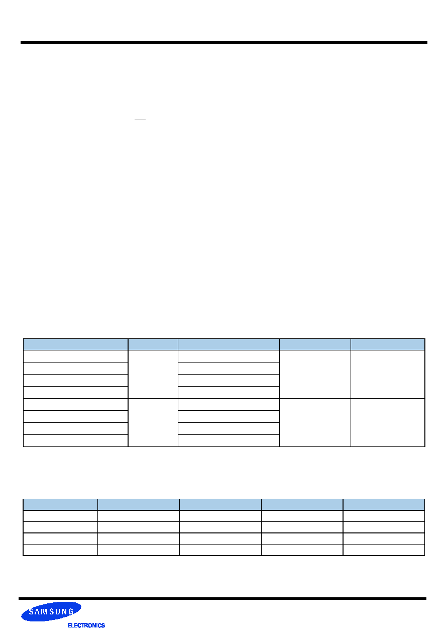
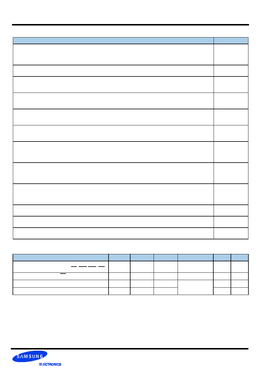
DM is internally loaded to match DQ and DQS identically.
Row & Column address configuration
Organization
Row Address
Column Address
64Mx8
A0~A12
A0-A9, A11
32Mx16
A0~A12
A0-A9
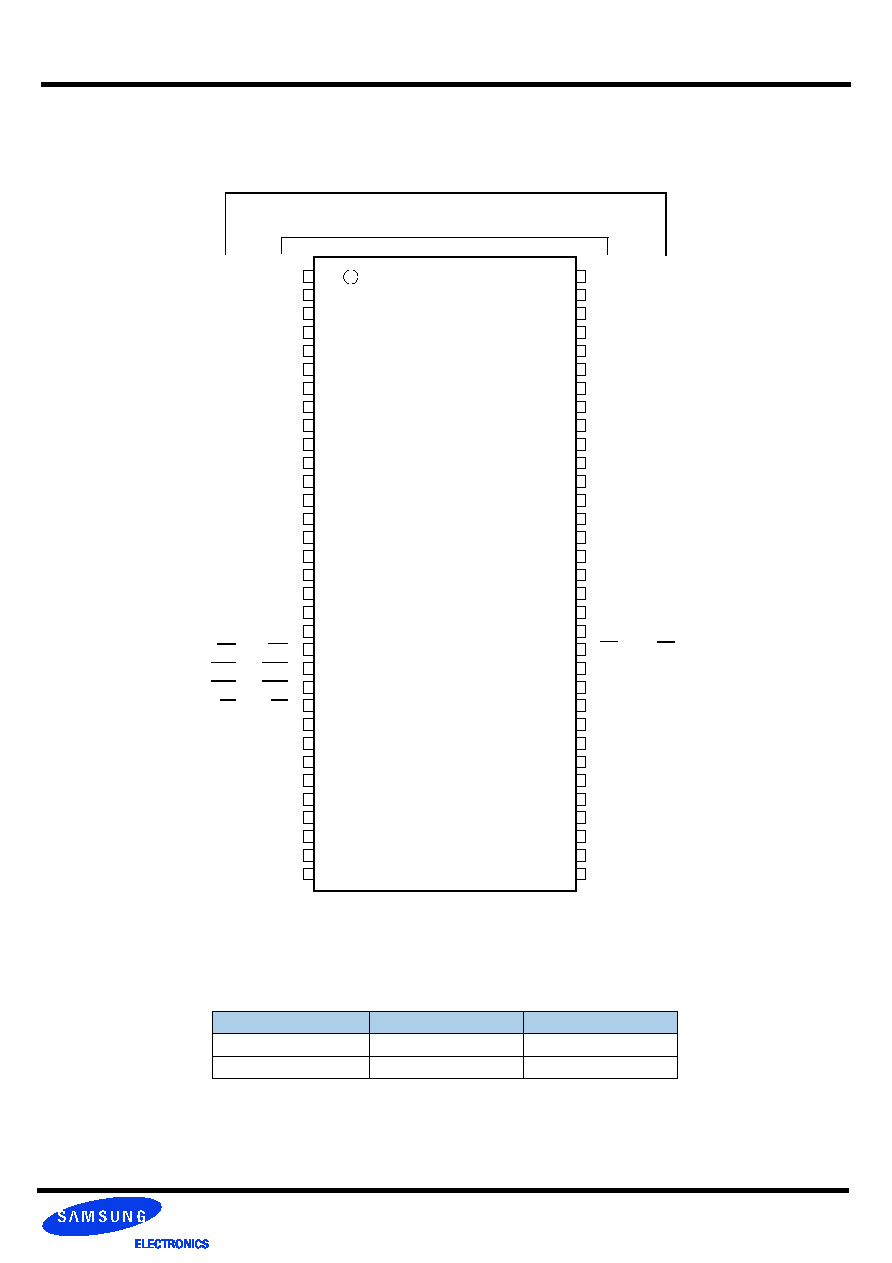
4.0 Pin Description
512Mb TSOP-II Package Pinout
V
DD
1
66Pin TSOPII
(400mil x 875mil)
DQ
0
2
V
DDQ
3
NC
4
DQ
1
5
V
SSQ
6
NC
7
DQ
2
8
V
DDQ
9
NC
10
DQ
3
11
V
SSQ
12
BA
0
20
CS
19
RAS
18
CAS
17
WE
16
NC
15
V
DDQ
14
NC
13
V
DD
27
A
3
26
A
2
25
A
1
24
A
0
23
AP/A
10
22
BA
1
21
V
SS
54
DQ
7
53
V
SSQ
52
NC
51
DQ
6
50
V
DDQ
49
NC
48
DQ
5
47
V
SSQ
46
NC
45
DQ
4
44
V
DDQ
43
A
11
35
36
CKE
37
CK
38
DM
39
V
REF
40
V
SSQ
41
NC
42
V
SS
55
A
4
56
A
5
57
A
6
58
A
7
59
A
8
60
A
9
34
(0.65mm Pin Pitch)
33
32
31
30
29
28
61
62
63
64
65
66
NC
NC
NC
NC
NC
V
DD
NC
DQS
NC
V
SS
CK
NC
A
12
Bank Address
BA0~BA1
Auto Precharge
A10
32Mb x 16
V
DD
DQ
0
V
DDQ
DQ
1
DQ
2
V
SSQ
DQ
3
DQ
4
V
DDQ
DQ
5
DQ
6
V
SSQ
BA
0
CS
RAS
CAS
WE
LDM
V
DDQ
DQ
7
V
DD
A
3
A
2
A
1
A
0
AP/A
10
BA
1
NC
LDQS
NC
NC
NC
V
DD
V
SS
DQ
15
V
SSQ
DQ
14
DQ
13
V
DDQ
DQ
12
DQ
11
V
SSQ
DQ
10
DQ
9
V
DDQ
A
11
CKE
CK
UDM
V
REF
V
SSQ
DQ
8
V
SS
A
4
A
5
A
6
A
7
A
8
A
9
NC
UDQS
NC
V
SS
CK
NC
A
12
64Mb x 8
Rev. 0.3 June. 2005
DDR SDRAM
DDR SDRAM 512Mb D-die (x8, x16)
Preliminary
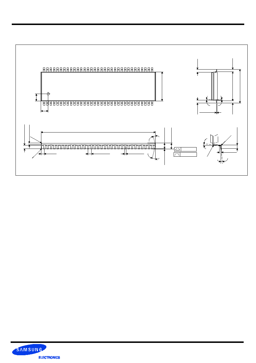
Units : Millimeters
0.30�0.08
0.65TYP
(0.71)
22.22�0.10
0.125
(0.
80)
10
.16
�
0.
10
0�~8�
#1
#33
#66
#34
(1.50)
(1
.50
)
0.65�0.08
1.
00
�
0.1
0
1.
20MA
X
(0.
50)
(0.
50)
(10
.
16
)
11
.
7
6
�
0.
2
0
(10�)
(10�)
+0.075
-0.035
(0
.
8
0
)
0.10 MAX
0.075 MAX
[
]
0.
05 MI
N
(10�)
(10�)
(R0.1
5)
0.
2
1
0
�
0.
05
0.
6
6
5
�
0.
05
(R
0.
15)
(4
�)
(R
0.
25
)
(R
0.2
5)
0.
45
~0.7
5
0.25TYP
NOTE
1. ( ) IS REFERENCE
2. [ ] IS ASS'Y OUT QUALITY
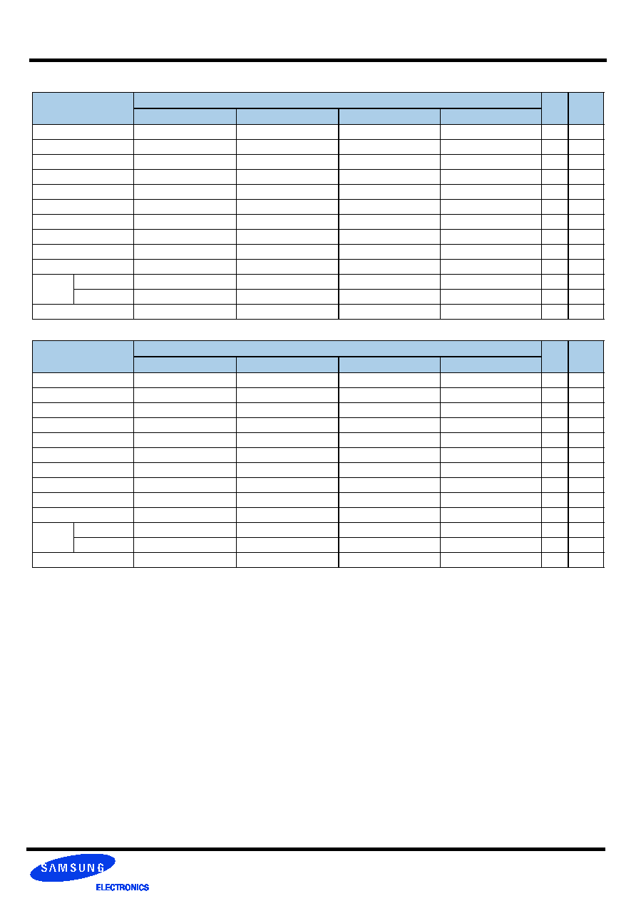
66pin TSOPII / Package dimension
5.0 Package Physical Dimension
Rev. 0.3 June. 2005
DDR SDRAM
DDR SDRAM 512Mb D-die (x8, x16)
Preliminary
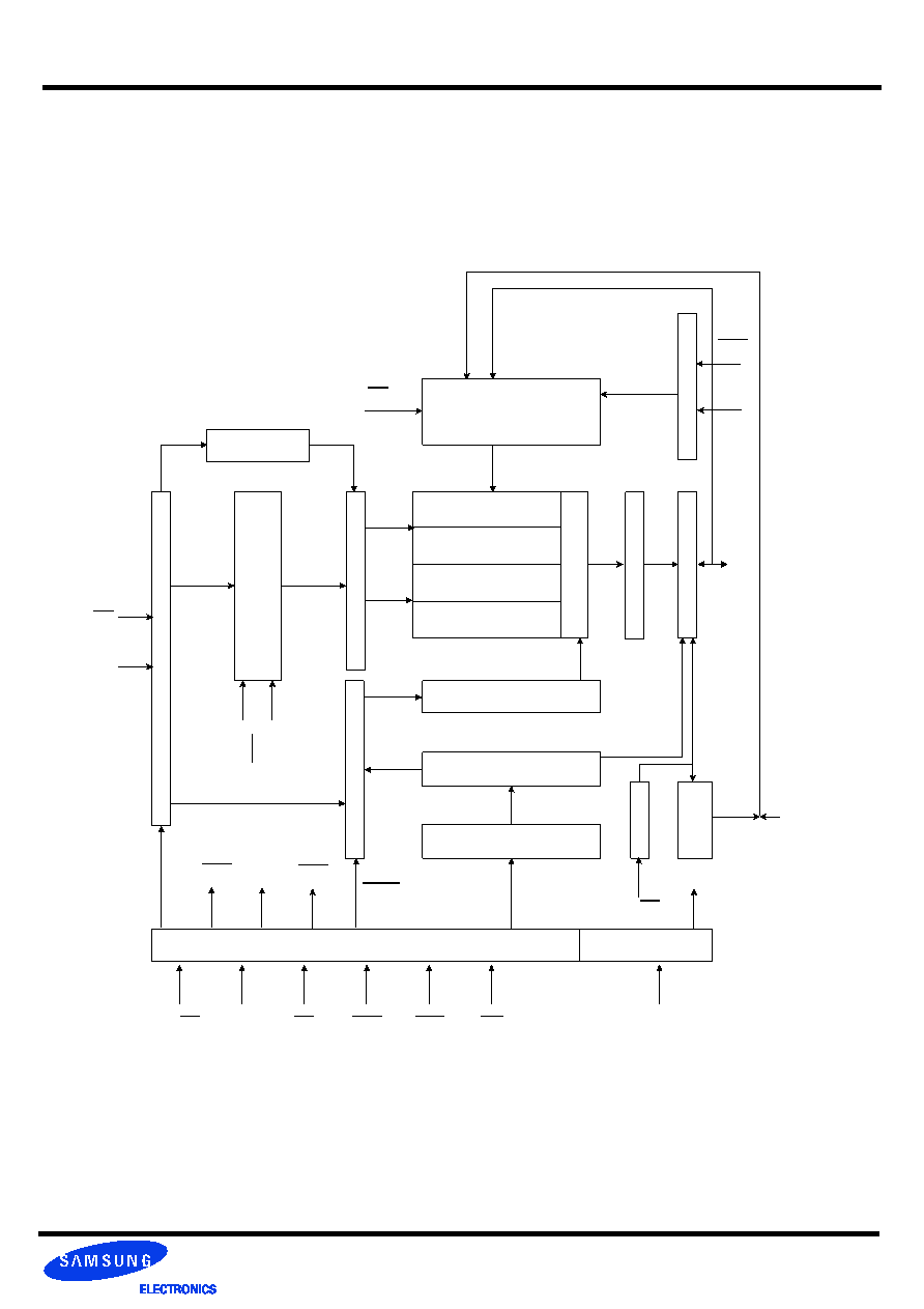
6.0 Block Diagram (
16Mb x 8 / 8Mb x 16
I/O x4 Banks)
Bank Select
Timing Register
Address Register
Re
fre
s
h
C
ounter
Ro
w Bu
f
f
e
r
Ro
w Decode
r
Co
l. Buf
f
er
Data Input Register
Serial to parallel
8Mx16/ 4Mx32
8Mx16/ 4Mx32
8Mx16/ 4Mx32
Se
ns
e AMP
2
-
bit p
r
efetch
O
u
tput
Buf
f
er
I/
O Control
Column Decoder
Latency & Burst Length
Programming Register
DL
L
St
r
o
b
e
Gen.
CK, CK
ADD
LCKE
CK, CK
CKE
CS
RAS
CAS
WE
CK, CK
LCAS
LRAS LCBR
LWE
LWCBR
LR
AS
LCBR
CK, CK
x8/16/32
x16/32
x8/16
x8/16
LWE
LDM (x8)
x8/16
DQi
Data Strobe
LUDM (x16)
LDM (x8)
LUDM (x16)
DM Input Register
LDM (x8)
LUDM (x16)
8Mx16/ 4Mx32
Rev. 0.3 June. 2005
DDR SDRAM
DDR SDRAM 512Mb D-die (x8, x16)
Preliminary
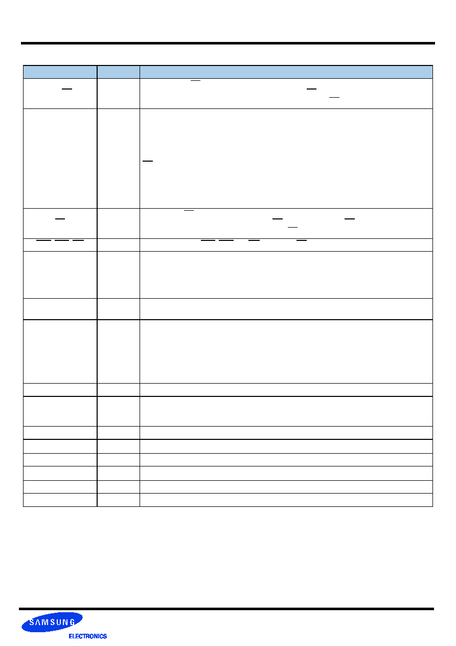
SYMBOL
TYPE
DESCRIPTION
CK, CK
Input
Clock : CK and CK are differential clock inputs. All address and control input signals are sam-
pled on the positive edge of CK and negative edge of CK. Output (read) data is referenced to
both edges of CK. Internal clock signals are derived from CK/CK.
CKE
Input
Clock Enable : CKE HIGH activates, and CKE LOW deactivates internal clock signals, and
device input buffers and output drivers. Taking CKE Low provides PRECHARGE POWER-
DOWN and SELF REFRESH operation (all banks idle), or ACTIVE POWER-DOWN (row
ACTIVE in any bank). CKE is synchronous for POWER-DOWN entry and exit, and for SELF
REFRESH entry. CKE is asynchronous for SELF REFRESH exit, and for output disable. CKE
must be maintained high throughput READ and WRITE accesses. Input buffers, excluding CK,
CK and CKE are disabled during POWER-DOWN. Input buffers, excluding CKE are disabled
during SELF REFRESH. CKE is an SSTL_2 input, but will detect an LVCMOS Low level after
Vdd is applied upon 1st power up, After V
REF
has become stable during the power on and ini-
tialization sequence, it must be maintained for proper operation of the CKE receiver. For
proper SELF-REFRESH entry and exit, V
REF
must be maintained to this input.
CS
Input
Chip Select : CS enables(registered LOW) and disables(registered HIGH) the command
decoder. All commands are masked when CS is registered HIGH. CS provides for external
bank selection on systems with multiple banks. CS is considered part of the command code.
RAS, CAS, WE
Input
Command Inputs : RAS, CAS and WE (along with CS) define the command being entered.
LDM,(UDM)
Input
Input Data Mask : DM is an input mask signal for write data. Input data is masked when DM is
sampled HIGH along with that input data during a WRITE access. DM is sampled on both
edges of DQS. Although DM pins are input only, the DM loading matches the DQ and DQS
loading. For the x16, LDM corresponds to the data on DQ0~D7 ; UDM corresponds to the data
on DQ8~DQ15. DM may be driven high, low, or floating during READs.
BA0, BA1
Input
Bank Addres Inputs : BA0 and BA1 define to which bank an ACTIVE, READ, WRITE or PRE-
CHARGE command is being applied.
A [0 : 12]
Input
Address Inputs : Provide the row address for ACTIVE commands, and the column address and
AUTO PRECHARGE bit for READ/WRITE commands, to select one location out of the mem-
ory array in the respective bank. A10 is sampled during a PRECHARGE command to deter-
mine whether the PRECHARGE applies to one bank (A10 LOW) or all banks (A10 HIGH). If
only one bank is to be precharged, the bank is selected by BA0, BA1. The address inputs also
provide the op-code during a MODE REGISTER SET command. BA0 and BA1 define which
mode register is loaded during the MODE REGISTER SET command (MRS or EMRS).
DQ
I/O
Data Input/Output : Data bus
LDQS,(U)DQS
I/O
Data Strobe : Output with read data, input with write data. Edge-aligned with read data, cen-
tered in write data. Used to capture write data. For the x16, LDQS corresponds to the data on
DQ0~D7 ; UDQS corresponds to the data on DQ8~DQ15
NC
-
No Connect : No internal electrical connection is present.
VDDQ
Supply
DQ Power Supply : +2.5V � 0.2V. (+2.6V �0.1V for DDR400)
VSSQ
Supply
DQ Ground.
VDD
Supply
Power Supply : +2.5V � 0.2V. (+2.6V �0.1V for DDR400)
VSS
Supply
Ground.
VREF
Input
SSTL_2 reference voltage.
7.0 Input/Output Function Description
Rev. 0.3 June. 2005
DDR SDRAM
DDR SDRAM 512Mb D-die (x8, x16)
Preliminary
(V=Valid, X=Don
t Care, H=Logic High, L=Logic Low)
Note :
1. OP Code : Operand Code. A
0
~ A
13
& BA
0
~ BA
1
: Program keys. (@EMRS/MRS)
2. EMRS/MRS can be issued only at all banks precharge state.
A new command can be issued 2 clock cycles after EMRS or MRS.
3. Auto refresh functions are same as the CBR refresh of DRAM.
The automatical precharge without row precharge command is meant by "Auto".
Auto/self refresh can be issued only at all banks precharge state.
4. BA
0
~ BA
1
: Bank select addresses.
If both BA
0
and BA
1
are "Low" at read, write, row active and precharge, bank A is selected.
If BA
0
is "High" and BA
1
is "Low" at read, write, row active and precharge, bank B is selected.
If BA
0
is "Low" and BA
1
is "High" at read, write, row active and precharge, bank C is selected.
If both BA
0
and BA
1
are "High" at read, write, row active and precharge, bank D is selected.
5. If A
10
/AP is "High" at row precharge, BA
0
and BA
1
are ignored and all banks are selected.
6. During burst write with auto precharge, new read/write command can not be issued.
Another bank read/write command can be issued after the end of burst.
New row active of the associated bank can be issued at t
RP
after the end of burst.
7. Burst stop command is valid at every burst length.
8. DM(x4/8) sampled at the rising and falling edges of the DQS and Data-in are masked at the both edges (Write DM latency is 0).
UDM/LDM(x16 only) sampled at the rising and falling edges of the UDQS/LDQS and Data-in are masked at the both edges
(Write UDM/LDM latency is 0).
9. This combination is not defined for any function, which means "No Operation(NOP)" in DDR SDRAM.
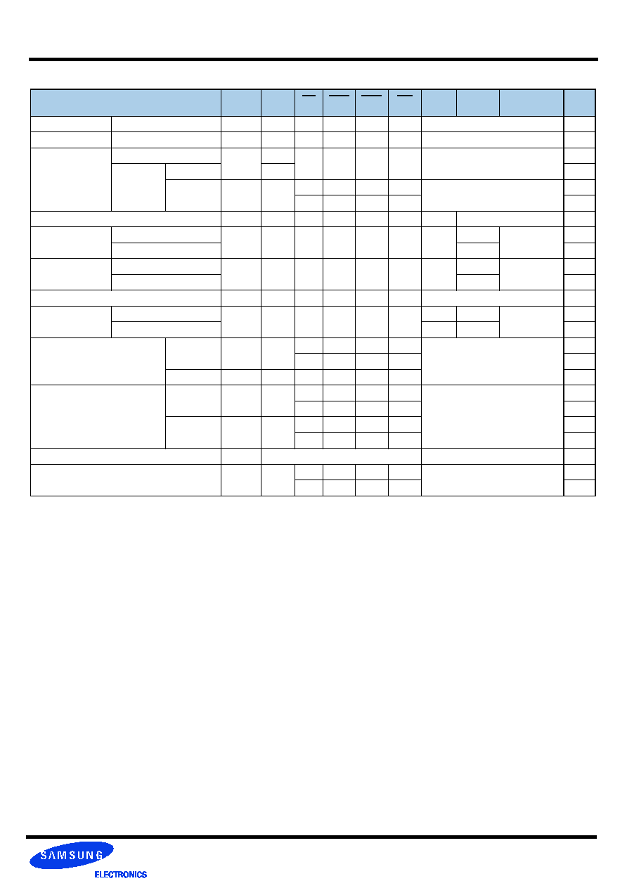
COMMAND
CKEn-1 CKEn
CS
RAS
CAS
WE
BA0,1 A10/AP
A0 ~ A9,
A11 ~ A12
Note
Register
Extended MRS
H
X
L
L
L
L
OP CODE
1, 2
Register
Mode Register Set
H
X
L
L
L
L
OP CODE
1, 2
Refresh
Auto Refresh
H
H
L
L
L
H
X
3
Self
Refresh
Entry
L
3
Exit
L
H
L
H
H
H
X
3
H
X
X
X
3
Bank Active & Row Addr.
H
X
L
L
H
H
V
Row Address
Read &
Column Address
Auto Precharge Disable
H
X
L
H
L
H
V
L
Column
Address
4
Auto Precharge Enable
H
4
Write &
Column Address
Auto Precharge Disable
H
X
L
H
L
L
V
L
Column
Address
4
Auto Precharge Enable
H
4, 6
Burst Stop
H
X
L
H
H
L
X
7
Precharge
Bank Selection
H
X
L
L
H
L
V
L
X
All Banks
X
H
5
Active Power Down
Entry
H
L
H
X
X
X
X
L
V
V
V
Exit
L
H
X
X
X
X
Precharge Power Down Mode
Entry
H
L
H
X
X
X
X
L
H
H
H
Exit
L
H
H
X
X
X
L
V
V
V
DM(UDM/LDM for x16 only)
H
X
X
8
No operation (NOP) : Not defined
H
X
H
X
X
X
X
9
L
H
H
H
9
8.0 Command Truth Table
Rev. 0.3 June. 2005
DDR SDRAM
DDR SDRAM 512Mb D-die (x8, x16)
Preliminary
16M x 8Bit x 4 Banks / 8M x 16Bit x 4 Banks Double Data Rate SDRAM
The K4H510838D / K4H511638D is 536,870,912 bits of double data rate synchronous DRAM organized as 4x 16,777,216 / 4x
8,388,608 words by 8/16bits, fabricated with SAMSUNG
s high performance CMOS technology. Synchronous features with Data Strobe
allow extremely high performance up to 400Mb/s per pin. I/O transactions are possible on both edges of DQS. Range of operating fre-
quencies, programmable burst length and programmable latencies allow the device to be useful for a variety of high performance mem-
ory system applications.
Note : Permanent device damage may occur if ABSOLUTE MAXIMUM RATINGS are exceeded.
Functional operation should be restricted to recommend operation condition.
Exposure to higher than recommended voltage for extended periods of time could affect device reliability.
Parameter
Symbol
Value
Unit
Voltage on any pin relative to V
SS
V
IN
, V
OUT
-0.5 ~ 3.6
V
Voltage on V
DD
& V
DDQ
supply relative to V
SS
V
DD
, V
DDQ
-1.0 ~ 3.6
V
Storage temperature
T
STG
-55 ~ +150
�C
Power dissipation
P
D
1.5
W
Short circuit current
I
OS
50
mA
Recommended operating conditions(Voltage referenced to V
SS
=0V, T
A
=0 to 70
�C)
Note :
1. VREF is expected to be equal to 0.5*VDDQ of the transmitting device, and to track variations in the dc level of same. Peak-to peak noise on VREF may
not exceed +/-2% of the dc value.
2. V
TT
is not applied directly to the device. V
TT
is a system supply for signal termination resistors, is expected to be set equal to VREF, and must track vari-
ations in the DC level of VREF
3. VID is the magnitude of the difference between the input level on CK and the input level on CK.
4. The ratio of the pullup current to the pulldown current is specified for the same temperature and voltage, over the entire temperature and voltage range,
for device drain to source voltages from 0.25V to 1.0V. For a given output, it represents the maximum difference between pullup and pulldown drivers
due to process variation. The full variation in the ratio of the maximum to minimum pullup and pulldown current will not exceed 1.7 for device drain to
source voltages from 0.1 to 1.0.
Parameter
Symbol
Min
Max
Unit
Note
Supply voltage(for device with a nominal V
DD
of 2.5V for DDR266/333)
V
DD
2.3
2.7
Supply voltage(for device with a nominal V
DD
of 2.6V for DDR400)
V
DD
2.5
2.7
I/O Supply voltage(for device with a nominal V
DD
of 2.5V for DDR266/333)
V
DDQ
2.3
2.7
V
I/O Supply voltage(for device with a nominal V
DD
of 2.5V for DDR400)
V
DDQ
2.5
2.7
I/O Reference voltage
V
REF
0.49*VDDQ
0.51*VDDQ
V
1
I/O Termination voltage(system)
V
TT
V
REF
-0.04
V
REF
+0.04
V
2
Input logic high voltage
V
IH
(DC)
V
REF
+0.15
V
DDQ
+0.3
V
Input logic low voltage
V
IL
(DC)
-0.3
V
REF
-0.15
V
Input Voltage Level, CK and CK inputs
V
IN
(DC)
-0.3
V
DDQ
+0.3
V
Input Differential Voltage, CK and CK inputs
V
ID
(DC)
0.36
V
DDQ
+0.6
V
3
V-I Matching: Pullup to Pulldown Current Ratio
VI(Ratio)
0.71
1.4
-
4
Input leakage current
I
I
-2
2
uA
Output leakage current
I
OZ
-5
5
uA
Output High Current(Normal strengh driver) ;V
OUT
= V
TT
+ 0.84V
I
OH
-16.8
mA
Output High Current(Normal strengh driver) ;V
OUT
= V
TT
- 0.84V
I
OL
16.8
mA
Output High Current(Half strengh driver) ;V
OUT
= V
TT
+ 0.45V
I
OH
-9
mA
Output High Current(Half strengh driver) ;V
OUT
= V
TT
- 0.45V
I
OL
9
mA
9.0 General Description
10.0 Absolute Maximum Rating
11.0 DC Operating Conditions
Rev. 0.3 June. 2005
DDR SDRAM
DDR SDRAM 512Mb D-die (x8, x16)
Preliminary
Conditions
Symbol
Operating current - One bank Active-Precharge;
tRC=tRCmin; tCK=10ns for DDR200, tCK=7.5ns for DDR266, 6ns for DDR333, 5ns for DDR400;
DQ,DM and DQS inputs changing once per clock cycle;
address and control inputs changing once every two clock cycles.
IDD0
Operating current - One bank operation ; One bank open, BL=4, Reads
- Refer to the following page for detailed test condition
IDD1
Precharge power-down standby current; All banks idle; power - down mode;
CKE = <VIL(max); tCK=10ns for DDR200,tCK=7.5ns for DDR266, 6ns for DDR333, 5ns for DDR400;
Vin = Vref for DQ,DQS and DM.
IDD2P
Precharge Floating standby current; CS# > =VIH(min);All banks idle; CKE > = VIH(min); tCK=10ns for
DDR200,tCK=7.5ns for DDR266, 6ns for DDR333, 5ns for DDR400; Address and other control inputs changing
once per clock cycle; Vin = Vref for DQ,DQS and DM
IDD2F
Precharge Quiet standby current; CS# > = VIH(min); All banks idle;
CKE > = VIH(min); tCK=10ns for DDR200, tCK=7.5ns for DDR266, 6ns for DDR333, 5ns for DDR400; Address and
other control inputs stable at >= VIH(min) or =<VIL(max); Vin = Vref for DQ ,DQS and DM
IDD2Q
Active power - down standby current ; one bank active; power-down mode;
CKE=< VIL (max); tCK=10ns for DDR200,tCK=7.5ns for DDR266, 6ns for DDR333, 5ns for DDR400;
Vin = Vref for DQ,DQS and DM
IDD3P
Active standby current; CS# >= VIH(min); CKE>=VIH(min);
one bank active; active - precharge; tRC=tRASmax; tCK=10ns for DDR200,tCK=7.5ns for DDR266, 6ns for
DDR333, 5ns for DDR400; DQ, DQS and DM inputs changing twice per clock cycle; address and other control
inputs changing once per clock cycle
IDD3N
Operating current - burst read; Burst length = 2; reads; continguous burst; One bank active; address and control
inputs changing once per clock cycle; CL=2 at tCK=10ns for DDR200, CL=2 at 7.5ns for DDR266(A2), CL=2.5 at
tCK=7.5ns for DDR266(B0), tCK=6ns for DDR333, CL=3 at tCK=5ns for DDR400; 50% of data changing on every
transfer; lout = 0 m A
IDD4R
Operating current - burst write; Burst length = 2; writes; continuous burst;
One bank active address and control inputs changing once per clock cycle; CL=2 at tCK=10ns for DDR200, CL=2
at tCK=7.5ns for DDR266(A2), CL=2.5 at tCK=7.5ns for DDR266(B0), 6ns for DDR333, 5ns for DDR400; DQ, DM
and DQS inputs changing twice per clock cycle, 50% of input data changing at every burst
IDD4W
Auto refresh current; tRC = tRFC(min) which is 12*tCK for DDR200 at tCK=10ns; 16*tCK for DDR266 at
tCK=7.5ns; 20*tCK for DDR333 at tCK=6ns, 24*tCK for DDR400 at tCK=5ns; distributed refresh
IDD5
Self refresh current; CKE =< 0.2V; External clock on; tCK=10ns for DDR200, tCK=7.5ns for DDR266, 6ns for
DDR333, 5ns for DDR400.
IDD6
Operating current - Four bank operation ; Four bank interleaving with BL=4
-Refer to the following page for detailed test condition
IDD7A
( T
A
= 25
�C, f=100MHz)
Note :
1.These values are guaranteed by design and are tested on a sample basis only.
2. Although DM is an input -only pin, the input capacitance of this pin must model the input capacitance of the DQ and DQS pins.
This is required to match signal propagation times of DQ, DQS, and DM in the system.
3. Unused pins are tied to ground.
4. This parameteer is sampled. For DDR266 and DDR333 VDDQ = +2.5V +0.2V, VDD = +3.3V +0.3V or +0.25V+0.2V. For
DDR400, VDDQ = +2.6V +0.1V, VDD = +2.6V +0.1V. For all devices, f=100MHz, tA=25
�C, Vout(dc) = VDDQ/2, Vout(peak to
peak) = 0.2V. DM inputs are grouped with I/O pins - reflecting the fact that they are matched in loading (to facilitate trace
matching at the board level).
Parameter
Symbol
Min
Max
DeltaCap(max)
Unit
Note
Input capacitance
(A0 ~ A12, BA0 ~ BA1, CKE, CS, RAS,CAS, WE)
CIN1
2
3
0.5
pF
4
Input capacitance( CK, CK )
CIN2
2
3
0.25
pF
4
Data & DQS input/output capacitance
COUT
4
5
0.5
pF
1,2,3,4
Input capacitance(DM for x4/8, UDM/LDM for x16)
CIN3
4
5
pF
1,2,3,4
12.0 DDR SDRAM Spec Items & Test Conditions
13.0 Input/Output Capacitance

Rev. 0.3 June. 2005
DDR SDRAM
DDR SDRAM 512Mb D-die (x8, x16)
Preliminary
IDD7A : Operating current: Four bank operation
1. Typical Case: Fro DDR200,266,333: Vdd = 2.5V, T=25'C; For DDR400: Vdd=2.6V,T=25'C
Worst Case : Vdd = 2.7V, T= 10' C
2. Four banks are being interleaved with tRC(min), Burst Mode, Address and Control inputs on NOP edge are not
changing. lout = 0mA
4. Timing patterns
- B0(133Mhz, CL=2.5) : tCK = 7.5ns, CL=2.5, BL=4, tRRD = 2*tCK, tRCD = 3*tCK, Read with autoprecharge
Read : A0 N A1 R0 A2 R1 A3 R2 N R3 A0 N A1 R0 - repeat the same timing with random address changing
*50% of data changing at every burst
- A2(133Mhz, CL=2) : tCK = 7.5ns, CL2=2, BL=4, tRRD = 2*tCK, tRCD = 3*tCK, Read with autoprecharge
Read : A0 N A1 R0 A2 R1 A3 R2 N R3 A0 N A1 R0 - repeat the same timing with random address changing
*50% of data changing at every burst
- B3(166Mhz,CL=2.5) : tCK=6ns, CL=2.5, BL=4, tRRD=2*tCK, tRCD=3*tCK, Read with autoprecharge
Read : A0 N A1 R0 A2 R1 A3 R2 N R3 A0 N A1 R0 - repeat the same timing with random address changing
*50% of data changing at every burst
- CC(200Mhz,CL = 3) : tCK = 5ns, CL = 3, BL = 4, tRCD = 3*tCK , tRC = 11*tCK, tRAS = 8*tCK
Read : A0 N N R0 N N N N P0 N N - repeat the same timing with random address changing
*50% of data changing at every transfer
Legend : A=Activate, R=Read, W=Write, P=Precharge, N=DESELECT
IDD1 : Operating current: One bank operation
1. Typical Case: Fro DDR200,266,333: Vdd = 2.5V, T=25'C; For DDR400: Vdd=2.6V,T=25'C
Worst Case : Vdd = 2.7V, T= 10'c
2. Only one bank is accessed with tRC(min), Burst Mode, Address and Control inputs on NOP edge are changing once
per clock cycle. lout = 0mA
3. Timing patterns
- B0(133Mhz, CL=2.5) : tCK = 7.5ns, CL=2.5, BL=4, tRCD = 3*tCK, tRC = 9*tCK, tRAS = 6*tCK
Read : A0 N N R0 N N P0 N N A0 N - repeat the same timing with random address changing
*50% of data changing at every burst
- A2 (133Mhz, CL=2) : tCK = 7.5ns, CL=2, BL=4, tRCD = 3*tCK, tRC = 9*tCK, tRAS = 6*tCK
Read : A0 N N R0 N N P0 N N A0 N - repeat the same timing with random address changing
*50% of data changing at every burst
- B3(166Mhz, CL=2.5) : tCK=6ns, CL=2.5, BL=4, tRCD=3*tCK, tRC = 10*tCK, tRAS=7*tCK
Read : A0 N N R0 N N P0 N N A0 N - repeat the same timing with random address changing
*50% of data changing at every burst
- CC(200Mhz,CL = 3) : tCK = 5ns, CL = 3, BL = 4, tRCD = 3*tCK , tRC = 11*tCK, tRAS = 8*tCK
Read : A0 N N R0 N N N N P0 N N - repeat the same timing with random address changing
*50% of data changing at every transfer
Legend : A=Activate, R=Read, W=Write, P=Precharge, N=DESELECT
14.0 Detailed test condition for DDR SDRAM IDD1 & IDD7A
Rev. 0.3 June. 2005
DDR SDRAM
DDR SDRAM 512Mb D-die (x8, x16)
Preliminary
(V
DD
=2.7V, T = 10
�C)
Symbol
64Mx8 (K4H510838D)
Unit Notes
CC(DDR400@CL=3) B3(DDR333@CL=2.5) A2(DDR266@CL=2.0) B0(DDR266@CL=2.5)
IDD0
120
105
95
95
mA
IDD1
150
135
125
125
mA
IDD2P
5
5
5
5
mA
IDD2F
30
30
30
30
mA
IDD2Q
25
25
25
25
mA
IDD3P
45
30
30
30
mA
IDD3N
60
45
45
45
mA
IDD4R
155
140
125
125
mA
IDD4W
175
150
130
130
mA
IDD5
220
205
195
195
mA
IDD6
Normal
5
5
5
5
mA
Low power
3
3
3
3
mA Optional
IDD7A
385
360
325
325
mA
Symbol
32Mx16 (K4H511638D)
Unit Notes
CC(DDR400@CL=3) B3(DDR333@CL=2.5) A2(DDR266@CL=2.0) B0(DDR266@CL=2.5)
IDD0
120
105
95
95
mA
IDD1
160
140
130
130
mA
IDD2P
5
5
5
5
mA
IDD2F
30
30
30
30
mA
IDD2Q
25
25
25
25
mA
IDD3P
45
30
30
30
mA
IDD3N
60
45
45
45
mA
IDD4R
190
170
155
155
mA
IDD4W
215
185
160
160
mA
IDD5
220
205
195
195
mA
IDD6
Normal
5
5
5
5
mA
Low power
3
3
3
3
mA Optional
IDD7A
400
380
345
345
mA
15.0 DDR SDRAM IDD spec table
Rev. 0.3 June. 2005
DDR SDRAM
DDR SDRAM 512Mb D-die (x8, x16)
Preliminary
Note :
1. VID is the magnitude of the difference between the input level on CK and the input level on /CK.
2. The value of VIX is expected to equal 0.5*VDDQ of the transmitting device and must track variations in the dc level of the same.
Parameter/Condition
Symbol
Min
Max
Unit
Note
Input High (Logic 1) Voltage, DQ, DQS and DM signals
VIH(AC)
VREF + 0.31
V
Input Low (Logic 0) Voltage, DQ, DQS and DM signals.
VIL(AC)
VREF - 0.31
V
Input Differential Voltage, CK and /CK inputs
VID(AC)
0.7
VDDQ+0.6
V
1
Input Crossing Point Voltage, CK and /CK inputs
VIX(AC)
0.5*VDDQ-0.2
0.5*VDDQ+0.2
V
2
Parameter
Specification
DDR400
DDR333
DDR200/266
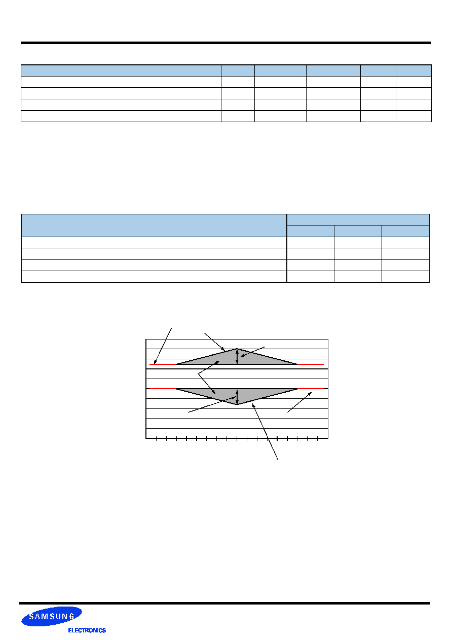
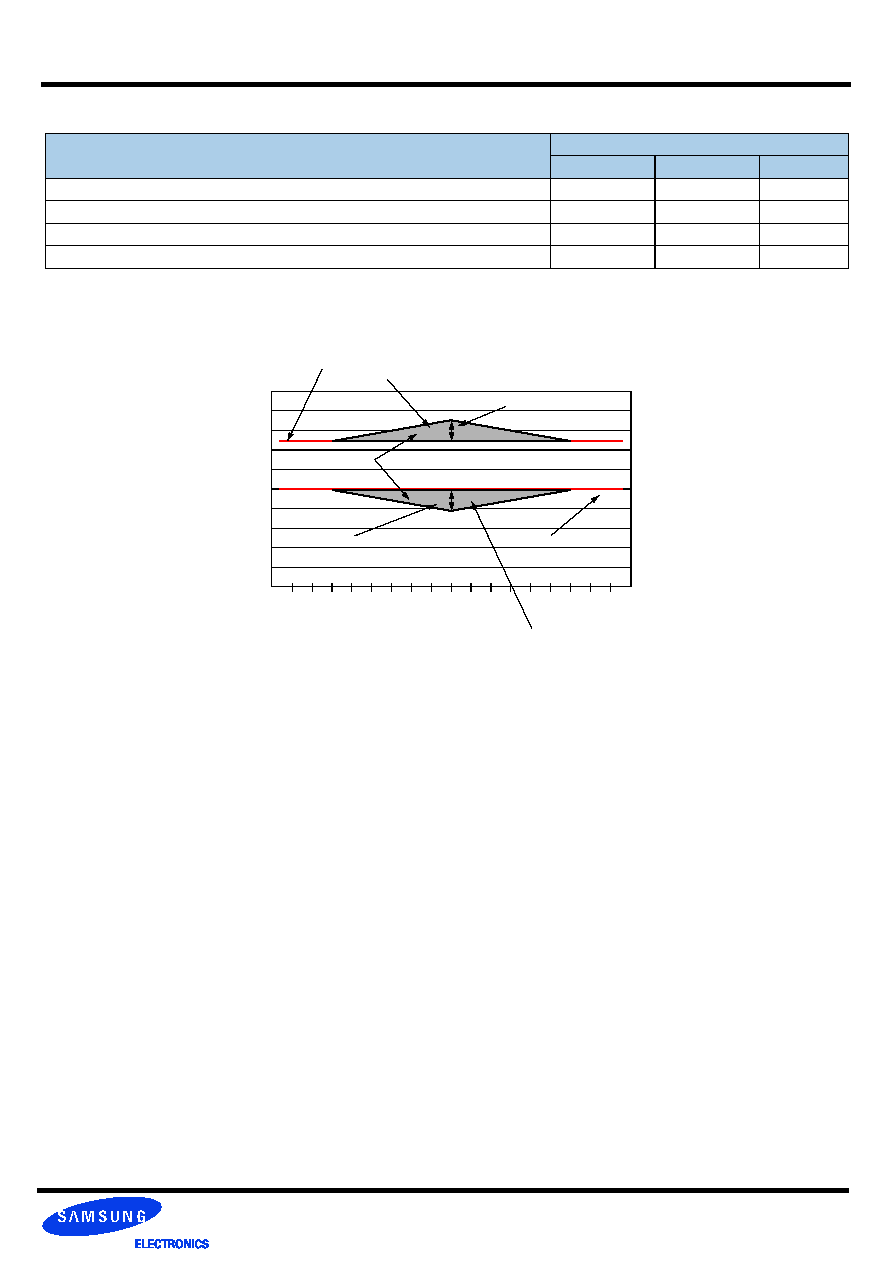
Maximum peak amplitude allowed for overshoot
TBD
TBD
1.5 V
Maximum peak amplitude allowed for undershoot
TBD
TBD
1.5 V
The area between the overshoot signal and VDD must be less than or equal to
TBD
TBD
4.5 V-ns
The area between the undershoot signal and GND must be less than or equal to
TBD
TBD
4.5 V-ns
5
4
3
2
1
0
-1
-2
-3
-4
-5
0
0.5
0.6875
1.0
1.5
2.0
2.5
3.0
3.5
4.0
4.5
5.0
5.5
6.0
6.3125
6.5
7.0
VDD
Overshoot
Maximum Amplitude = 1.5V
Area = 4.5V-ns
Maximum Amplitude = 1.5V
undershoot
GND
Vo
l
t
s
(
V
)
Tims(ns)
AC overshoot/Undershoot Definition
16.0 AC Operating Conditions
17.0 AC Overshoot/Undershoot specification for Address and Control Pins
Rev. 0.3 June. 2005
DDR SDRAM
DDR SDRAM 512Mb D-die (x8, x16)
Preliminary
Parameter
Specification
DDR400
DDR333
DDR200/266
Maximum peak amplitude allowed for overshoot
TBD
TBD
1.2 V
Maximum peak amplitude allowed for undershoot
TBD
TBD
1.2 V
The area between the overshoot signal and VDD must be less than or equal to
TBD
TBD
2.4 V-ns
The area between the undershoot signal and GND must be less than or equal to
TBD
TBD
2.4 V-ns
5
4
3
2
1
0
-1
-2
-3
-4
-5
0 0.5 1.0 1.42 1.5 2.0 2.5 3.0 3.5 4.0 4.5 5.0 5.5 5.68 6.0 6.5 7.0
VDDQ
Overshoot
Maximum Amplitude = 1.2V
Area = 2.4V-ns
Maximum Amplitude = 1.2V
undershoot
GND
V
o
lt
s (V
)
Tims(ns)
DQ/DM/DQS AC overshoot/Undershoot Definition
18.0 Overshoot/Undershoot specification for Data, Strobe and Mask Pins
Rev. 0.3 June. 2005
DDR SDRAM
DDR SDRAM 512Mb D-die (x8, x16)
Preliminary
Parameter
Symbol
CC
(DDR400@CL=3.0)
B3
(DDR333@CL=2.5)
A2
(DDR266@CL=2.0)
B0
(DDR266@CL=2.5) Unit
Note
Min
Max
Min
Max
Min
Max
Min
Max
Row cycle time
tRC
55
60
65
65
ns
Refresh row cycle time
tRFC
70
72
75
75
ns
Row active time
tRAS
40
70K
42
70K
45
70K
45
70K
ns
RAS to CAS delay
tRCD
15
18
20
20
ns
Row precharge time
tRP
15
18
20
20
ns
Row active to Row active delay
tRRD
10
12
15
15
ns
Write recovery time
tWR
15
15
15
15
ns
Last data in to Read command
tWTR
2
1
1
1
tCK
Clock cycle time
CL=2.0
tCK
-
-
7.5
12
7.5
12
10
12
ns
CL=2.5
6
12
6
12
7.5
12
7.5
12
ns
CL=3.0
5
10
-
-
-
-
-
-
Clock high level width
tCH
0.45
0.55
0.45
0.55
0.45
0.55
0.45
0.55
tCK
Clock low level width
tCL
0.45
0.55
0.45
0.55
0.45
0.55
0.45
0.55
tCK
DQS-out access time from CK/CK
tDQSCK
-0.55
+0.55
-0.6
+0.6
-0.75
+0.75
-0.75
+0.75
ns
Output data access time from CK/CK
tAC
-0.65
+0.65
-0.7
+0.7
-0.75
+0.75
-0.75
+0.75
ns
Data strobe edge to ouput data edge
tDQSQ
-
0.4
-
0.45
-
0.5
-
0.5
ns
22
Read Preamble
tRPRE
0.9
1.1
0.9
1.1
0.9
1.1
0.9
1.1
tCK
Read Postamble
tRPST
0.4
0.6
0.4
0.6
0.4
0.6
0.4
0.6
tCK
CK to valid DQS-in
tDQSS
0.72
1.28
0.75
1.25
0.75
1.25
0.75
1.25
tCK
DQS-in setup time
tWPRES
0
0
0
0
ns
13
DQS-in hold time
tWPRE
0.25
0.25
0.25
0.25
tCK
DQS falling edge to CK rising-setup time
tDSS
0.2
0.2
0.2
0.2
tCK
DQS falling edge from CK rising-hold time
tDSH
0.2
0.2
0.2
0.2
tCK
DQS-in high level width
tDQSH
0.35
0.35
0.35
0.35
tCK
DQS-in low level width
tDQSL
0.35
0.35
0.35
0.35
tCK
Address and Control Input setup time(fast)
tIS
0.6
0.75
0.9
0.9
ns
15, 17~19
Address and Control Input hold time(fast)
tIH
0.6
0.75
0.9
0.9
ns
15, 17~19
Address and Control Input setup
tIS
0.7
0.8
1.0
1.0
ns
16~19
Address and Control Input hold time(slow)
tIH
0.7
0.8
1.0
1.0
ns
16~19
Data-out high impedence time from CK/CK
tHZ
-0.65
+0.65
-0.7
+0.7
-0.75
+0.75
-0.75
+0.75
ns
11
Data-out low impedence time from CK/CK
tLZ
-0.65
+0.65
-0.7
+0.7
-0.75
+0.75
-0.75
+0.75
ns
11
Mode register set cycle time
tMRD
10
12
15
15
ns
DQ & DM setup time to DQS
tDS
0.4
0.45
0.5
0.5
ns
j, k
DQ & DM hold time to DQS
tDH
0.4
0.45
0.5
0.5
ns
j, k
Control & Address input pulse width
tIPW
2.2
2.2
2.2
2.2
ns
18
DQ & DM input pulse width
tDIPW
1.75
1.75
1.75
1.75
ns
18
Exit self refresh to non-Read command
tXSNR
75
75
75
75
ns
Exit self refresh to read command
tXSRD
200
200
200
200
tCK
Refresh interval time
tREFI
7.8
7.8
7.8
7.8
us
14
Output DQS valid window
tQH
tHP
-tQHS
-
tHP
-tQHS
-
tHP
-tQHS
-
tHP
-tQHS
-
ns
21
Clock half period
tHP
tCLmin
or tCHmin
-
tCLmin
or tCHmin
-
tCLmin
or tCHmin
-
tCLmin
or tCHmin
-
ns
20, 21
Data hold skew factor
tQHS
0.5
0.55
0.75
0.75
ns
21
DQS write postamble time
tWPST
0.4
0.6
0.4
0.6
0.4
0.6
0.4
0.6
tCK
12
Active to Read with Auto precharge
command
tRAP
15 18 20
20
Autoprecharge write recovery +
Precharge time
tDAL
(tWR/tCK)
+
(tRP/tCK)
(tWR/tCK)
+
(tRP/tCK)
(tWR/tCK)
+
(tRP/tCK)
(tWR/tCK)
+
(tRP/tCK)
tCK
23
19.0 AC Timming Parameters & Specifications
Rev. 0.3 June. 2005
DDR SDRAM
DDR SDRAM 512Mb D-die (x8, x16)
Preliminary
The following specification parameters are required in systems using DDR333, DDR266 & DDR200 devices to ensure proper system
performance. these characteristics are for system simulation purposes and are guaranteed by design.
Table 1 : Input Slew Rate for DQ, DQS, and DM
Table 2 : Input Setup & Hold Time Derating for Slew Rate
Table 3 : Input/Output Setup & Hold Time Derating for Slew Rate
Table 4 : Input/Output Setup & Hold Derating for Rise/Fall Delta Slew Rate
Table 5 : Output Slew Rate Characteristice (X4, X8 Devices only)
Table 6 : Output Slew Rate Characteristice (X16 Devices only)
Table 7 : Output Slew Rate Matching Ratio Characteristics
AC CHARACTERISTICS
DDR333
DDR266
DDR200
PARAMETER
SYMBOL
MIN
MAX
MIN
MAX
MIN
MAX
Units
Notes
DQ/DM/DQS input slew rate measured between
VIH(DC), VIL(DC) and VIL(DC), VIH(DC)
DCSLEW
TBD
TBD
TBD
TBD
0.5
4.0
V/ns
a, m
Input Slew Rate
tIS
tIH
Units
Notes
0.5 V/ns
0
0
ps
i
0.4 V/ns
+50
0
ps
i
0.3 V/ns
+100
0
ps
i
Input Slew Rate
tDS
tDH
Units
Notes
0.5 V/ns
0
0
ps
k
0.4 V/ns
+75
+75
ps
k
0.3 V/ns
+150
+150
ps
k
Delta Slew Rate
tDS
tDH
Units
Notes
+/- 0.0 V/ns
0
0
ps
j
+/- 0.25 V/ns
+50
+50
ps
j
+/- 0.5 V/ns
+100
+100
ps
j
Slew Rate Characteristic
Typical Range
(V/ns)
Minimum
(V/ns)
Maximum
(V/ns)
Notes
Pullup Slew Rate
1.2 ~ 2.5
1.0
4.5
a,c,d,f,g,h
Pulldown slew
1.2 ~ 2.5
1.0
4.5
b,c,d,f,g,h
Slew Rate Characteristic
Typical Range
(V/ns)
Minimum
(V/ns)
Maximum
(V/ns)
Notes
Pullup Slew Rate
1.2 ~ 2.5
0.7
5.0
a,c,d,f,g,h
Pulldown slew
1.2 ~ 2.5
0.7
5.0
b,c,d,f,g,h
AC CHARACTERISTICS
DDR266B
DDR200
PARAMETER
MIN
MAX
MIN
MAX
Notes
Output Slew Rate Matching Ratio (Pullup to Pulldown)
TBD
TBD
0.67
1.5
e,m
20.0 System Characteristics for DDR SDRAM

Rev. 0.3 June. 2005
DDR SDRAM
DDR SDRAM 512Mb D-die (x8, x16)
Preliminary
1. All voltages referenced to Vss.
2. Tests for ac timing, IDD, and electrical, ac and dc characteristics, may be conducted at nominal reference/supply voltage levels,
but the related specifications and device operation are guaranteed for the full voltage range specified.
3. Figure 1 represents the timing reference load used in defining the relevant timing parameters of the part. It is not intended to be
either a precise representation of the typical system environment nor a depiction of the actual load presented by a production
tester. System designers will use IBIS or other simulation tools to correlate the timing reference load to a system environment.
Manufacturers will correlate to their production test conditions (generally a coaxial transmission line terminated at the tester elec-
tronics).
4. AC timing and IDD tests may use a VIL to VIH swing of up to 1.5 V in the test environment, but input timing is still referenced to
VREF (or to the crossing point for CK/CK), and parameter specifications are guaranteed for the specified ac input levels under nor-
mal use conditions. The minimum slew rate for the input signals is 1 V/ns in the range between VIL(ac) and VIH(ac).
5. The ac and dc input level specifications are as defined in the SSTL_2 Standard (i.e., the receiver will effectively switch as a result
of the signal crossing the ac input level and will remain in that state as long as the signal does not ring back above (below) the dc
input LOW (HIGH) level.
6. Inputs are not recognized as valid until VREF stabilizes. Exception: during the period before VREF stabilizes, CKE
0.2VDDQ is
recognized as LOW.
7. Enables on.chip refresh and address counters.
8. IDD specifications are tested after the device is properly initialized.
9. The CK/CK input reference level (for timing referenced to CK/CK) is the point at which CK and CK cross; the input reference level
for signals other than CK/CK, is VREF.
10. The output timing reference voltage level is VTT.
11. tHZ and tLZ transitions occur in the same access time windows as valid data transitions. These parameters are not referenced to
a specific voltage level but specify when the device output is no longer driving (HZ), or begins driving (LZ).
12. The maximum limit for this parameter is not a device limit. The device will operate with a greater value for this parameter, but sys
tem performance (bus turnaround) will degrade accordingly.
13. The specific requirement is that DQS be valid (HIGH, LOW, or at some point on a valid transition) on or before this CK edge. A
valid transition is defined as monotonic and meeting the input slew rate specifications of the device. when no writes were previ
ously in progress on the bus, DQS will be tran sitioning from High- Z to logic LOW. If a previous write was in progress, DQS could
be HIGH, LOW, or transitioning from HIGH to LOW at this time, depending on tDQSS.
14. A maximum of eight AUTO REFRESH commands can be posted to any given DDR SDRAM device.
15. For command/address input slew rate
1.0 V/ns
16. For command/address input slew rate
0.5 V/ns and < 1.0 V/ns
Output
VDDQ
50
30pF
(Vout)
Figure 1 : Timing Reference Load
21.0 Component Notes

Rev. 0.3 June. 2005
DDR SDRAM
DDR SDRAM 512Mb D-die (x8, x16)
Preliminary
Component Notes
17. For CK & CK slew rate
1.0 V/ns
18. These parameters guarantee device timing, but they are not necessarily tested on each device. They may be guaranteed by
device design or tester correlation.
19. Slew Rate is measured between VOH(ac) and VOL(ac).
20. Min (tCL, tCH) refers to the smaller of the actual clock low time and the actual clock high time as provided to the device (i.e. this
value can be greater than the minimum specification limits for tCL and tCH).....For example, tCL and tCH are = 50% of the
period, less the half period jitter (tJIT(HP)) of the clock source, and less the half period jitter due to crosstalk (tJIT(crosstalk)) into
the clock traces.
21. tQH = tHP - tQHS, where:
tHP = minimum half clock period for any given cycle and is defined by clock high or clock low (tCH, tCL). tQHS accounts for 1) The
pulse duration distortion of on-chip clock circuits; and 2) The worst case push-out of DQS on one tansition followed by the worst
case pull-in of DQ on the next transition, both of which are, separately, due to data pin skew and output pattern effects, and p-
channel to n-channel variation of the output drivers.
22. tDQSQ
Consists of data pin skew and output pattern effects, and p-channel to n-channel variation of the output drivers for any given cycle.
23. tDAL = (tWR/tCK) + (tRP/tCK)
For each of the terms above, if not already an integer, round to the next highest integer. Example: For DDR266B at CL=2.5 and
tCK=7.5ns tDAL = (15 ns / 7.5 ns) + (20 ns/ 7.5ns) = (2) + (3)
tDAL = 5 clocks
Rev. 0.3 June. 2005
DDR SDRAM
DDR SDRAM 512Mb D-die (x8, x16)
Preliminary
b. Pulldown slew rate is measured under the test conditions shown in Figure 3.
Output
Test point
VDDQ
50
Figure 3 : Pulldown slew rate test load
c. Pullup slew rate is measured between (VDDQ/2 - 320 mV +/- 250 mV)
Pulldown slew rate is measured between (VDDQ/2 + 320 mV +/- 250 mV)
Pullup and Pulldown slew rate conditions are to be met for any pattern of data, including all outputs switching and only one output
switching.
Example : For typical slew rate, DQ0 is switching
For minmum slew rate, all DQ bits are switching from either high to low, or low to high.
The remaining DQ bits remain the same as for previous state.
d. Evaluation conditions
Typical : 25
�C (T Ambient), VDDQ = 2.5V(for DDR266/333) and 2.6V(for DDR400), typical process
Minimum : 70
�C (T Ambient), VDDQ = 2.3V(for DDR266/333) and 2.5V(for DDR400), slow - slow process
Maximum : 0
�C (T Ambient), VDDQ = 2.7V(for DDR266/333) and 2.7V(for DDR400), fast - fast process
e. The ratio of pullup slew rate to pulldown slew rate is specified for the same temperature and voltage, over the entire temperature and
voltage range. For a given output, it represents the maximum difference between pullup and pulldown drivers due to process variation.
f. Verified under typical conditions for qualification purposes.
g. TSOPII package divices only.
h. Only intended for operation up to 266 Mbps per pin.
i. A derating factor will be used to increase tIS and tIH in the case where the input slew rate is below 0.5V/ns
as shown in Table 2. The Input slew rate is based on the lesser of the slew rates detemined by either VIH(AC) to VIL(AC) or
VIH(DC) to VIL(DC), similarly for rising transitions.
j. A derating factor will be used to increase tDS and tDH in the case where DQ, DM, and DQS slew rates differ, as shown in Tables 3 & 4.
Input slew rate is based on the larger of AC-AC delta rise, fall rate and DC-DC delta rise, Input slew rate is based on the lesser of the
slew rates determined by either VIH(AC) to VIL(AC) or VIH(DC) to VIL(DC), similarly for rising transitions.
The delta rise/fall rate is calculated as:
{1/(Slew Rate1)} - {1/(Slew Rate2)}
For example : If Slew Rate 1 is 0.5 V/ns and slew Rate 2 is 0.4 V/ns, then the delta rise, fall rate is - 0.5ns/V . Using the table given, this
would result in the need for an increase in tDS and tDH of 100 ps.
k. Table 3 is used to increase tDS and tDH in the case where the I/O slew rate is below 0.5 V/ns. The I/O slew rate is based on the lesser
on the lesser of the AC - AC slew rate and the DC- DC slew rate. The inut slew rate is based on the lesser of the slew rates deter
mined by either VIH(ac) to VIL(ac) or VIH(DC) to VIL(DC), and similarly for rising transitions.
m. DQS, DM, and DQ input slew rate is specified to prevent double clocking of data and preserve setup and hold times. Signal transi
tions through the DC region must be monotonic.
a. Pullup slew rate is characteristized under the test conditions as shown in Figure 2.
Output
Test point
VSSQ
50
Figure 2 : Pullup slew rate test load
22.0 System Notes
Rev. 0.3 June. 2005
DDR SDRAM
DDR SDRAM 512Mb D-die (x8, x16)
Preliminary
Figure 3. I/V characteristics for input/output buffers:Pull up(above) and pull down(below)
Maximum
Typical High
Minumum
Vout(V)
I
out
(mA)
- 2 2 0
- 2 0 0
- 1 8 0
- 1 6 0
- 1 4 0
- 1 2 0
- 1 0 0
- 8 0
- 6 0
- 4 0
- 2 0
0
0 .0
1 .0
2 .0
Minimum
Typical Low
Typical High
Maximum
0
20
40
60
80
100
120
140
160
0.0
0.5
1.0
1.5
2.0
2.5
Iout
(mA)
Typical Low
Vout(V)
Pullup Characteristics for Full Strength Output Driver
Pulldown Characteristics for Full Strength Output Driver
DDR SDRAM Output Driver V-I Characteristics
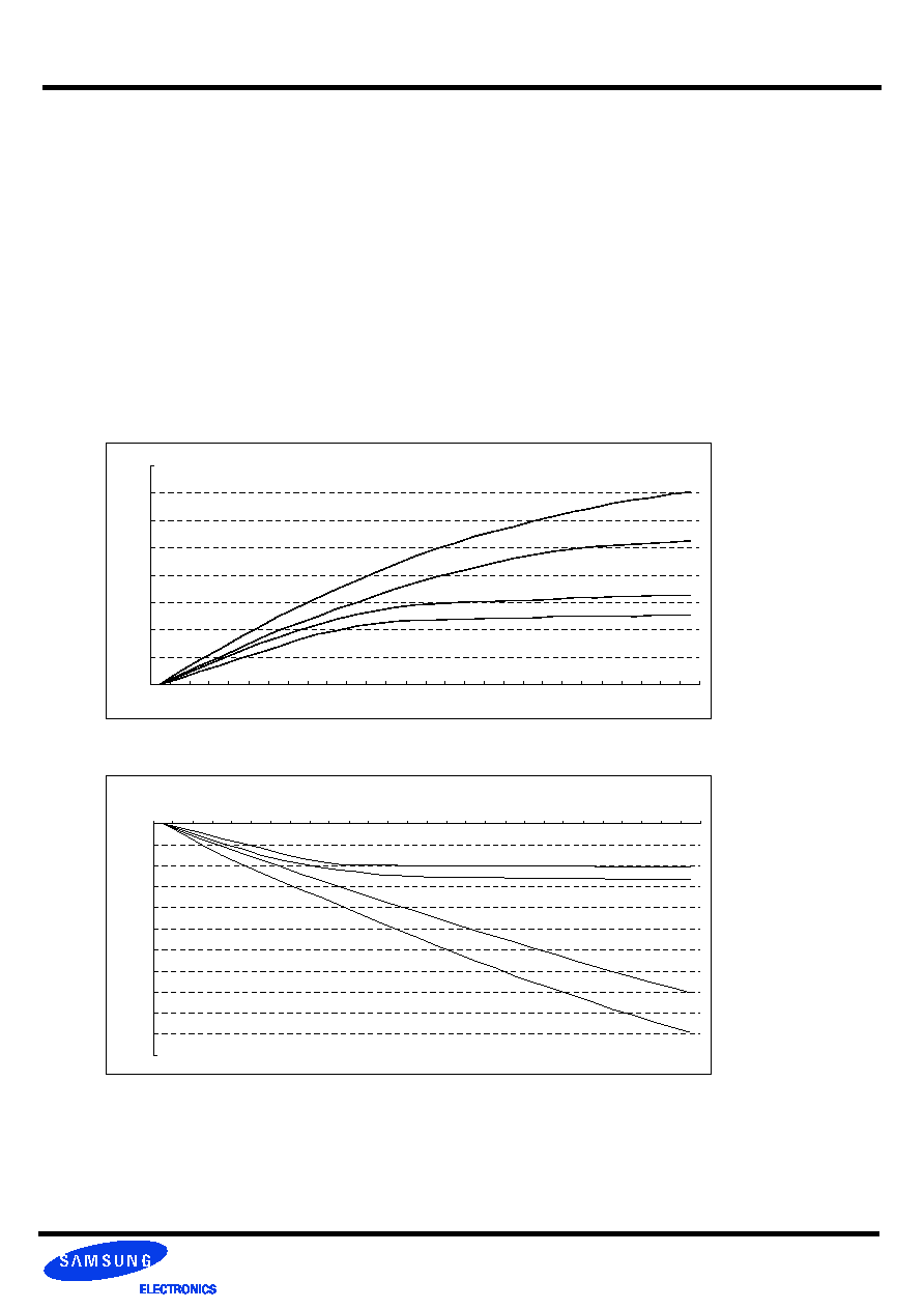
DDR SDRAM Output driver characteristics are defined for full and half strength operation as selected by the EMRS bit A1.
Figures 3 and 4 show the driver characteristics graphically, and tables 8 and 9 show the same data in tabular format suitable for input
into simulation tools. The driver characteristcs evaluation conditions are:
Output Driver Characteristic Curves Notes:
1. The full variation in driver current from minimum to maximum process, temperature and voltage will lie within the outer bounding lines
the of the V-I curve of Figure 3 and 4.
2. It is recommended that the "typical" IBIS V-I curve lie within the inner bounding lines of the V-I curves of Figure 3 and 4.
3. The full variation in the ratio of the "typical" IBIS pullup to "typical" IBIS pulldown current should be unity
+/-
10%, for device drain to
source voltages from 0.1 to1.0. This specification is a design objective only. It is not guaranteed.
Typical
25�C
Vdd/Vddq = 2.5V, typical process
Minimum
70�C
Vdd/Vddq = 2.3V, slow-slow process
Maximum
0�C
Vdd/Vddq = 2.7V, fast-fast process
23.0 IBIS : I/V Characteristics for Input and Output Buffers

Rev. 0.3 June. 2005
DDR SDRAM
DDR SDRAM 512Mb D-die (x8, x16)
Preliminary
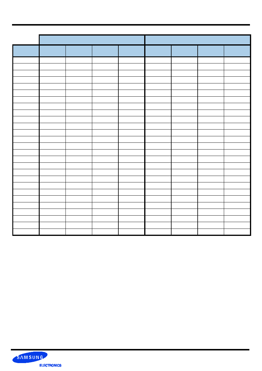
Table 8. Full Strength Driver Characteristics
Pulldown Current (mA)
pullup Current (mA)
Voltage
(V)
Typical
Low
Typical
High
Minimum
Maximum
Typical
Low
Typical
High
Minimum
Maximum
0.1
6.0
6.8
4.6
9.6
-6.1
-7.6
-4.6
-10.0
0.2
12.2
13.5
9.2
18.2
-12.2
-14.5
-9.2
-20.0
0.3
18.1
20.1
13.8
26.0
-18.1
-21.2
-13.8
-29.8
0.4
24.1
26.6
18.4
33.9
-24.0
-27.7
-18.4
-38.8
0.5
29.8
33.0
23.0
41.8
-29.8
-34.1
-23.0
-46.8
0.6
34.6
39.1
27.7
49.4
-34.3
-40.5
-27.7
-54.4
0.7
39.4
44.2
32.2
56.8
-38.1
-46.9
-32.2
-61.8
0.8
43.7
49.8
36.8
63.2
-41.1
-53.1
-36.0
-69.5
0.9
47.5
55.2
39.6
69.9
-41.8
-59.4
-38.2
-77.3
1.0
51.3
60.3
42.6
76.3
-46.0
-65.5
-38.7
-85.2
1.1
54.1
65.2
44.8
82.5
-47.8
-71.6
-39.0
-93.0
1.2
56.2
69.9
46.2
88.3
-49.2
-77.6
-39.2
-100.6
1.3
57.9
74.2
47.1
93.8
-50.0
-83.6
-39.4
-108.1
1.4
59.3
78.4
47.4
99.1
-50.5
-89.7
-39.6
-115.5
1.5
60.1
82.3
47.7
103.8
-50.7
-95.5
-39.9
-123.0
1.6
60.5
85.9
48.0
108.4
-51.0
-101.3
-40.1
-130.4
1.7
61.0
89.1
48.4
112.1
-51.1
-107.1
-40.2
-136.7
1.8
61.5
92.2
48.9
115.9
-51.3
-112.4
-40.3
-144.2
1.9
62.0
95.3
49.1
119.6
-51.5
-118.7
-40.4
-150.5
2.0
62.5
97.2
49.4
123.3
-51.6
-124.0
-40.5
-156.9
2.1
62.9
99.1
49.6
126.5
-51.8
-129.3
-40.6
-163.2
2.2
63.3
100.9
49.8
129.5
-52.0
-134.6
-40.7
-169.6
2.3
63.8
101.9
49.9
132.4
-52.2
-139.9
-40.8
-176.0
2.4
64.1
102.8
50.0
135.0
-52.3
-145.2
-40.9
-181.3
2.5
64.6
103.8
50.2
137.3
-52.5
-150.5
-41.0
-187.6
2.6
64.8
104.6
50.4
139.2
-52.7
-155.3
-41.1
-192.9
2.7
65.0
105.4
50.5
140.8
-52.8
-160.1
-41.2
-198.2
Rev. 0.3 June. 2005
DDR SDRAM
DDR SDRAM 512Mb D-die (x8, x16)
Preliminary
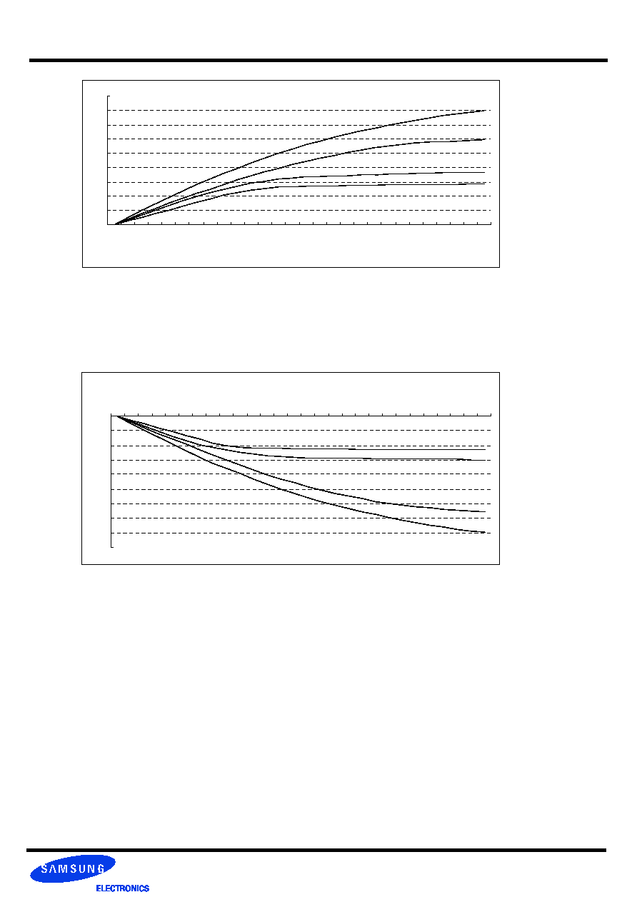
Figure 4. I/V characteristics for input/output buffers:Pull up(above) and pull down(below)
Maximum
Typical High
Minumum
Vout(V)
I
out
(mA)
-90
-80
-70
-60
-50
-40
-30
-20
-10
0
0.0
1.0
2.0
Iou
t
(m
A)
Minimum
Typical Low
Typical High
Maximum
0
10
20
30
40
50
60
70
80
90
0.0
1.0
2.0
I
out
(mA)
Typical Low
Vout(V)
Pullup Characteristics for Weak Output Driver
Pulldown Characteristics for Weak Output Driver
Rev. 0.3 June. 2005
DDR SDRAM
DDR SDRAM 512Mb D-die (x8, x16)
Preliminary
Pulldown Current (mA)
pullup Current (mA)
Voltage
(V)
Typical
Low
Typical
High
Minimum
Maximum
Typical
Low
Typical
High
Minimum
Maximum
0.1
3.4
3.8
2.6
5.0
-3.5
-4.3
-2.6
-5.0
0.2
6.9
7.6
5.2
9.9
-6.9
-8.2
-5.2
-9.9
0.3
10.3
11.4
7.8
14.6
-10.3
-12.0
-7.8
-14.6
0.4
13.6
15.1
10.4
19.2
-13.6
-15.7
-10.4
-19.2
0.5
16.9
18.7
13.0
23.6
-16.9
-19.3
-13.0
-23.6
0.6
19.6
22.1
15.7
28.0
-19.4
-22.9
-15.7
-28.0
0.7
22.3
25.0
18.2
32.2
-21.5
-26.5
-18.2
-32.2
0.8
24.7
28.2
20.8
35.8
-23.3
-30.1
-20.4
-35.8
0.9
26.9
31.3
22.4
39.5
-24.8
-33.6
-21.6
-39.5
1.0
29.0
34.1
24.1
43.2
-26.0
-37.1
-21.9
-43.2
1.1
30.6
36.9
25.4
46.7
-27.1
-40.3
-22.1
-46.7
1.2
31.8
39.5
26.2
50.0
-27.8
-43.1
-22.2
-50.0
1.3
32.8
42.0
26.6
53.1
-28.3
-45.8
-22.3
-53.1
1.4
33.5
44.4
26.8
56.1
-28.6
-48.4
-22.4
-56.1
1.5
34.0
46.6
27.0
58.7
-28.7
-50.7
-22.6
-58.7
1.6
34.3
48.6
27.2
61.4
-28.9
-52.9
-22.7
-61.4
1.7
34.5
50.5
27.4
63.5
-28.9
-55.0
-22.7
-63.5
1.8
34.8
52.2
27.7
65.6
-29.0
-56.8
-22.8
-65.6
1.9
35.1
53.9
27.8
67.7
-29.2
-58.7
-22.9
-67.7
2.0
35.4
55.0
28.0
69.8
-29.2
-60.0
-22.9
-69.8
2.1
35.6
56.1
28.1
71.6
-29.3
-61.2
-23.0
-71.6
2.2
35.8
57.1
28.2
73.3
-29.5
-62.4
-23.0
-73.3
2.3
36.1
57.7
28.3
74.9
-29.5
-63.1
-23.1
-74.9
2.4
36.3
58.2
28.3
76.4
-29.6
-63.8
-23.2
-76.4
2.5
36.5
58.7
28.4
77.7
-29.7
-64.4
-23.2
-77.7
2.6
36.7
59.2
28.5
78.8
-29.8
-65.1
-23.3
-78.8
2.7
36.8
59.6
28.6
79.7
-29.9
-65.8
-23.3
-79.7
Table 9. Weak Driver Characteristics