Äîêóìåíòàöèÿ è îïèñàíèÿ www.docs.chipfind.ru

DDR SDRAM
DDR SDRAM 256Mb E-die (x4, x8) Pb-Free
Rev. 1.1 October, 2004
256Mb E-die DDR SDRAM Specification
Revision 1.1
October, 2004
60 FBGA with Pb-Free
(RoHS compliant)
DDR SDRAM
DDR SDRAM 256Mb E-die (x4, x8) Pb-Free
Rev. 1.1 October, 2004
256Mb E-die Revision History
Revision 1.0 (February, 2004)
-First release
Revision 1.1 (October, 2004)
-Corrected typo.
DDR SDRAM
DDR SDRAM 256Mb E-die (x4, x8) Pb-Free
Rev. 1.1 October, 2004
· Double-data-rate architecture; two data transfers per clock cycle
· Bidirectional data strobe
[DQ] (x4,x8)
Four banks operation
· Differential clock inputs(CK and CK)
· DLL aligns DQ and DQS transition with CK transition
· MRS cycle with address key programs
-. Read latency 2, 2.5 (clock)
-. Burst length (2, 4, 8)
-. Burst type (sequential & interleave)
· All inputs except data & DM are sampled at the positive going edge of the system clock(CK)
· Data I/O transactions on both edges of data strobe
· Edge aligned data output, center aligned data input
· DM for write masking only (x4, x8)
· Auto & Self refresh
· 7.8us refresh interval(8K/64ms refresh)
· Maximum burst refresh cycle : 8
· 60Ball FBGA
Pb-Free
package
· RoHS compliant
*CL : CAS Latency
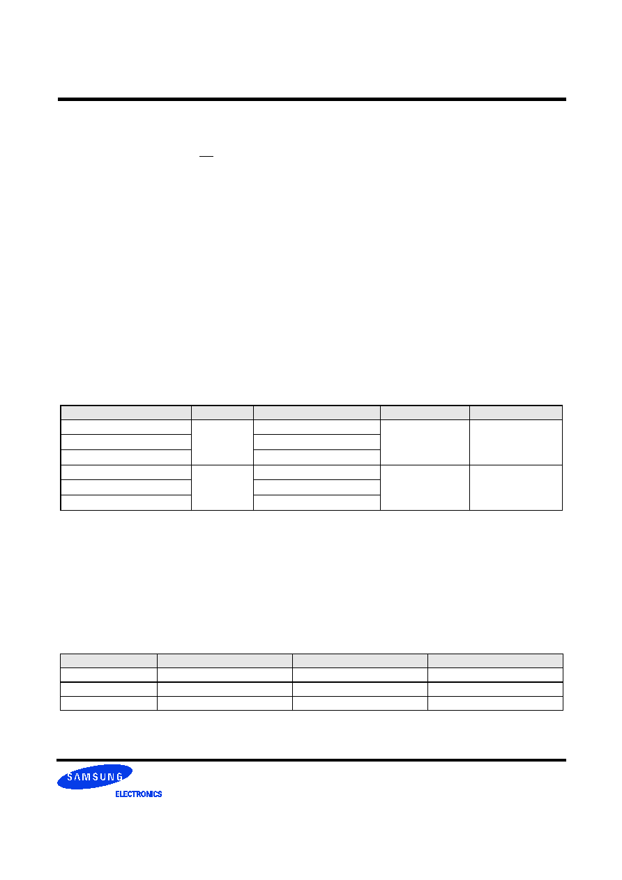
Operating Frequencies
B3(DDR333@CL=2.5)
A2(DDR266@CL=2)
B0(DDR266@CL=2.5)
CL-tRCD-tRP
2.5-3-3
2-3-3
2.5-3-3
Speed @CL2
133MHz
133MHz
100MHz
Speed @CL2.5
166MHz
133MHz
133MHz
Ordering Information
Part No.
Org.
Max Freq.
Interface
Package
K4H560438E-ZC/LB3
64M x 4
B3(DDR333@CL=2.5)
SSTL2
60 FBGA
K4H560438E-ZC/LA2
A2(DDR266@CL=2)
K4H560438E-ZC/LB0
B0(DDR266@CL=2.5)
K4H560838E-ZC/LB3
32M x 8
B3(DDR333@CL=2.5)
SSTL2
60 FBGA
K4H560838E-ZC/LA2
A2(DDR266@CL=2)
K4H560838E-ZC/LB0
B0(DDR266@CL=2.5)
Key Features
DDR SDRAM
DDR SDRAM 256Mb E-die (x4, x8) Pb-Free
Rev. 1.1 October, 2004
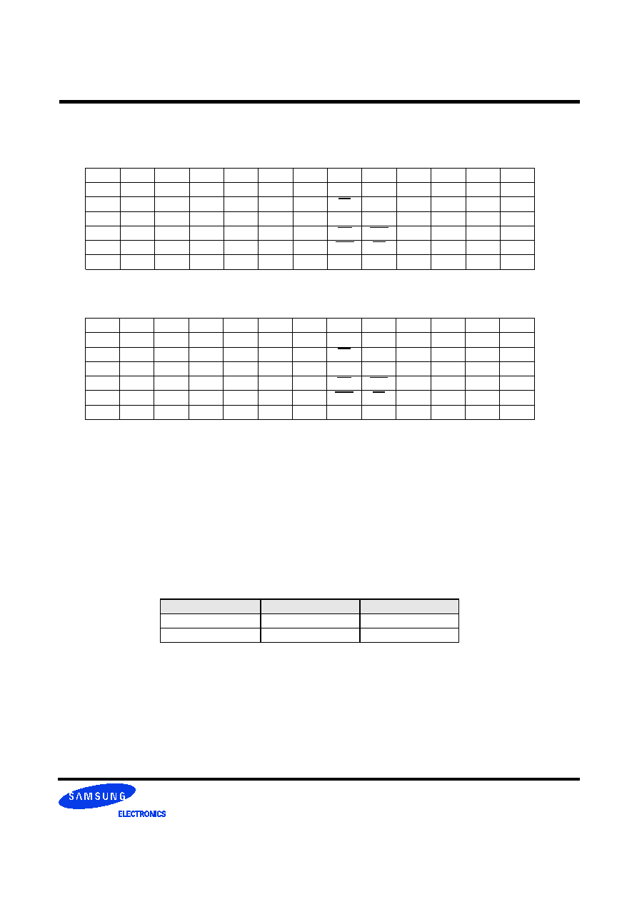
Ball Description
DM is internally loaded to match DQ and DQS identically.
Row & Column address configuration
Organization
Row Address
Column Address
64Mx4
A0~A12
A0-A9, A11
32Mx8
A0~A12
A0-A9
1
VSSQ
NC
NC
NC
NC
VREF
2
NC
VDDQ
VSSQ
VDDQ
VSSQ
VSS
CK
A12
A11
A8
A6
A4
3
VSS
DQ3
NC
DQ2
DQS
DM
CK
CKE
A9
A7
A5
VSS
A
B
C
D
E
F
G
H
J
K
L
M
7
VDD
DQ0
NC
DQ1
NC
NC
WE
RAS
BA1
A0
A2
VDD
8
NC
VSSQ
VDDQ
VSSQ
VDDQ
VDD
CAS
CS
BA0
A10/AP
A1
A3
9
VDDQ
NC
NC
NC
NC
NC
1
VSSQ
NC
NC
NC
NC
VREF
2
DQ7
VDDQ
VSSQ
VDDQ
VSSQ
VSS
CK
A12
A11
A8
A6
A4
3
VSS
DQ6
DQ5
DQ4
DQS
DM
CK
CKE
A9
A7
A5
VSS
A
B
C
D
E
F
G
H
J
K
L
M
7
VDD
DQ1
DQ2
DQ3
NC
NC
WE
RAS
BA1
A0
A2
VDD
8
DQ0
VSSQ
VDDQ
VSSQ
VDDQ
VDD
CAS
CS
BA0
A10/AP
A1
A3
9
VDDQ
NC
NC
NC
NC
NC
32M x 8bit
64M x 4bit
(
Bottom View
)
DDR SDRAM
DDR SDRAM 256Mb E-die (x4, x8) Pb-Free
Rev. 1.1 October, 2004
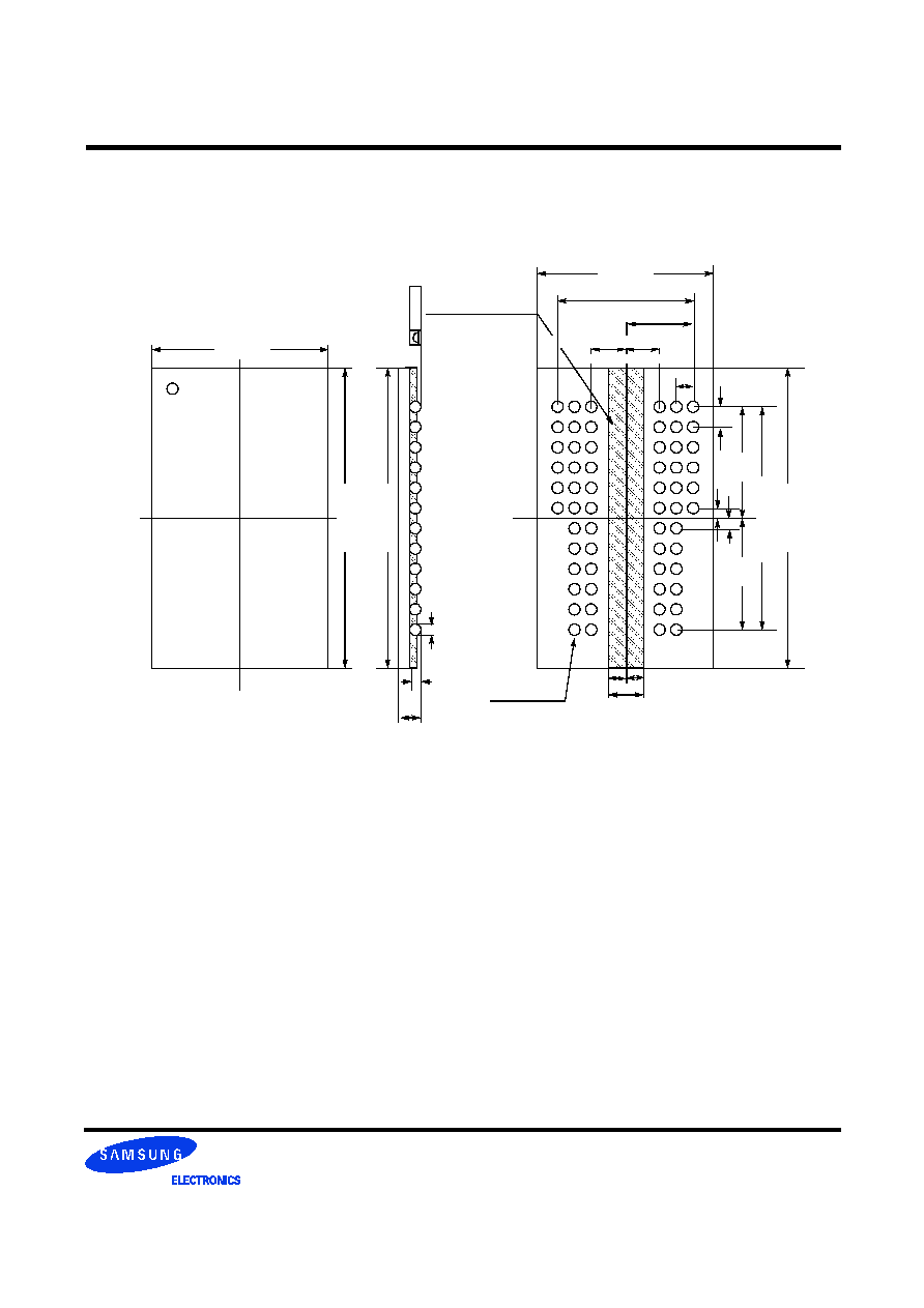
60Ball FBGA Package Dimension
Package Physical Dimension
( Unit : mm )
(0.90)
(0.90)
8.0 0
± 0.10
14.0
0
±
0.10
14.
0
±
0.
10
0
.
10 Max
0.4
5
±
0.0
5
0.35
± 0.05
1.10
± 0.10
1
2
3
4
5
6
7
8
9
ENCAPSULANT AREA
8.00
± 0.10
0.80 x 4 = 3.20
1.60
1.60
A
B
C
D
E
F
G
H
J
K
L
M
0.80
0.50
5.
5
0
1.0
0
x
11 =
11.0
0
14.0
0
±
0.10
5.
5
0
60 - 0.45
± 0.05
0.80 x 8 = 6.40
TOP VIEW
BOTTOM VIEW
(1.80)
0.50
1.00