
- 1 -
REV. 1.0 November. 2. 2000
128Mb DDR SDRAM
DDR SDRAM Specification
Version 1.0
- 2 -
REV. 1.0 November. 2. 2000
128Mb DDR SDRAM
Revision History
Version 0 (May, 1998)
- First version for internal review
Version 0.1(June, 1998)
- Added x4 organization
Version 0.2(Sep,1998)
1. Added "Issue prcharge command for all banks of the device" as the fourth step of power-up squence.
2. In power down mode timing diagram, NOP condition is added to precharge power down exit.
Version 0.3(Dec,1998)
- Added QFC Function.
- Added DC current value
- Reduce I/O capacitance values
Version 0.4(Feb,1999)
-Added DDR SDRAM history for reference(refer to the following page)
-Added low power version DC spec
Version 0.5(Apr,1999)
-Revised following first showing for JEDEC standard
-Added DC target current based on new DC test condition
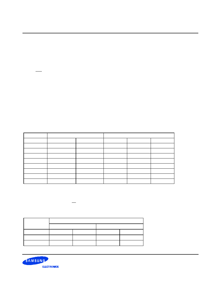
Version 0.6(July 1,1999)
1.Modified binning policy
From To
-Z (133Mhz) -Z (133Mhz/266Mbps@CL=2)
-8 (125Mhz) -Y (133Mhz/266Mbps@CL=2.5)
-0 (100Mhz) -0 (100Mhz/200Mbps@CL=2)
2.Modified the following AC spec values
*1
: Changed description method for the same functionality. This means no difference from the previous version.
3.Changed the following AC parameter symbol
From. To.
Output data access time from CK/CK tDQCK tAC
Version 0.61(August 9,1999)
- Changed the some values of "write with auto precharge" table for different bank in page 31.
From.
To.
-Z
-0
-Z
-Y
-0
tAC
+/- 0.75ns
+/- 1ns
+/- 0.75ns
+/- 0.75ns
+/- 0.8ns
tDQSCK
+/- 0.75ns
+/- 1ns
+/- 0.75ns
+/- 0.75ns
+/- 0.8ns
tDQSQ
+/- 0.5ns
+/- 0.75ns
+/- 0.5ns
+/- 0.5ns
+/- 0.6ns
tDS/tDH
0.5 ns
0.75 ns
0.5 ns
0.5 ns
0.6 ns
tCDLR
*1
2.5tCK-tDQSS
2.5tCK-tDQSS
1tCK
1tCK
1tCK
tPRE
*1
1tCK +/- 0.75ns
1tCK +/- 1ns
0.9/1.1 tCK
0.9/1.1 tCK
0.9/1.1 tCK
tRPST
*1
tCK/2 +/- 0.75ns
tCK/2 +/- 1ns
0.4/0.6 tCK
0.4/0.6 tCK
0.4/0.6 tCK
tHZQ
*1
tCK/2 +/- 0.75ns
tCK/2 +/- 1ns
+/- 0.75ns
+/- 0.75ns
+/-0.8ns
Asserted
command
For Different Bank
3
4
Old
New
Old
New
Read
Legal
Illegal
Legal
Illegal
Read + AP
*1
Legal
Illegal
Legal
Illegal
- 3 -
REV. 1.0 November. 2. 2000
128Mb DDR SDRAM
Revision History(continued)
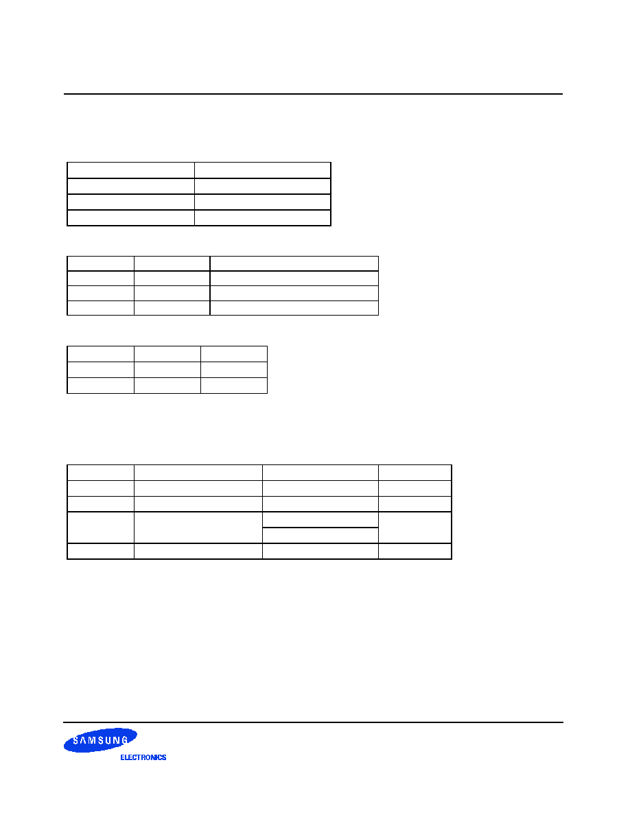
Version 0.7 (March, 2000)
- Changed 128Mb spec from target to Preliminary version.
- Changed partnames as follows.
- Changed input cap. spec.
- Changed operating condition.
- Added Overshoot/Undershoot spec
. Vih(max) = 4.2V, the overshoot voltage duration is
3ns at VDD.
. Vil(min) =- 1.5V, the overshoot voltage duration is
3ns at VSS.
- Changed AC parameters as follows.
- Added DC spec values.
Version 0.71 (April, 2000)
- Corrected a typo for tRAS at 133Mhz/CL2.5 from 48ns t0 45ns.
- Corrected a typo in "General Information" table from 64Mx4 to 8Mx16.
Version 0.72(May,2000)
- Changed DC spec item & test condition
Version 0.73(June,2000)
- Added updated DC spec values
- Deleted tDAL in AC parameter
Version 1.0(November,2000)
- Eliminate "preliminary"
from
to
KM44L32031BT-G(L)Z/Y/0
K4H280438B-TC(L)A2/B0/A0
KM48L16031BT-G(L)Z/Y/0
K4H280838B-TC(L)A2/B0/A0
KM416L8031BT-G(L)Z/Y/0
K4H281638B-TC(L)A2/B0/A0
from
to
CK/CK
2.5pF ~ 3.5pF
2.0pF ~ 3.0pF w/ Delta Cin = 0.25pF
DQ/DQS/DM
4.0pF ~ 5.5pF
4.0pF ~ 5.0pF w/ Delta Cin = 0.5pF
CMD/Addr
2.5pF ~ 3.5pF
2.0pF ~ 3.0pF with Delta Cin = 0.5pF
from
to
Vil/Vih(ac)
Vref +/- 0.35V
Vref +/- 0.31V
V
IL
/V
IH
(dc)
Vref +/- 0.18V
Vref +/- 0.15V
from
to
Comments
tDQSQ
+/- 0.5(PC266), +/- 0.6(PC200)
+0.5(PC266), +0.6(PC200)
tDV
+/- 0.35tCK
-
Removed
tQH
-
tHPmin - 0.75ns(PC266)
New Definition
tHPmin - 1.0ns(PC200)
tHP
-
tCLmin or tCHmin
New Definition

- 4 -
REV. 1.0 November. 2. 2000
128Mb DDR SDRAM
Contents
Revision History
General Information
1. Key Features
1.1 Features
1.2 Operating Frequencies
2. Package Pinout & Dimension
2.1 Package Pintout
2.2 Input/Output Function Description
2.3 66 Pin TSOP(II)/MS-024FC Package Physical Dimension
3. Functional Description
3.1 Simplified State Diagram
3.2 Basic Functionality
3.2.1 Power-Up Sequence
3.2.2 Mode Register Definition
3.2.2.1 Mode Register Set(MRS)
3.2.2.2 Extended Mode Register Set(EMRS)
3.2.3 Precharge
3.2.4 No Operation(NOP) & Device Deselect
3.2.5 Row Active
3.2.6 Read Bank
3.2.7 Write Bank
3.3 Essential Functionality for DDR SDRAM
3.3.1 Burst Read Operation
3.3.2 Burst Write Operation
3.3.3 Read Interrupted by a Read
3.3.4 Read Interrupted by a Write & Burst Stop
3.3.5 Read Interrupted by a Precharge
3.3.6 Write Interrupted by a Write
2
9
10
10
10
11
11
12
13
14
14
15
15
16
16
18
19
19
20
20
20
21
21
22
23
23
24
25

- 5 -
REV. 1.0 November. 2. 2000
128Mb DDR SDRAM
3.3.7 Write Interrupted by a Read & DM
3.3.8 Write Interrupted by a Precharge & DM
3.3.9 Burst Stop
3.3.10 DM masking
3.3.11 Read With Auto Precharge
3.3.12 Write With Auto Precharge
3.3.13 Auto Refresh & Self Refresh
3.3.14 Power Down
4. Command Truth Table
5. Functional Truth Table
6. Absolute Maximum Rating
7. DC Operating Conditions & Specifications
7.1 DC Operating Conditions
7.2 DC Specifications
8. AC Operating Conditions & Timming Specification
8.1 AC Operating Conditions
8.2 AC Timming Parameters & Specification
9. AC Operating Test Conditions
10. Input/Output Capacitance
11. IBIS: I/V Characteristics for Input and Output Buffers
11.1 Normal strength driver
11.2 Half strength driver( will be included in the future)
12. QFC function
QFC definition
QFC timming on Read Operation
QFC timming on Write operation with tDQSSmax
QFC timming on Write operation with tDQSSmin
QFC timming example for interrupted writes operation
Timing Diagram
26
27
28
29
30
31
32
33
34
35
40
40
41
42
42
43
45
45
46
46
48
49
49
49
50
50
51
52