- 1 -
256Mb
DDR SDRAM
Rev. 2.2 Mar. '03
∑ Double-data-rate architecture; two data transfers per clock cycle
∑ Bidirectional data strobe(DQS)
∑ Four banks operation
∑ Differential clock inputs(CK and CK)
∑ DLL aligns DQ and DQS transition with CK transition
∑ MRS cycle with address key programs
-. Read latency 2, 2.5 (clock)
-. Burst length (2, 4, 8)
-. Burst type (sequential & interleave)
∑ All inputs except data & DM are sampled at the positive going edge of the system clock(CK)
∑ Data I/O transactions on both edges of data strobe
∑ Edge aligned data output, center aligned data input
∑ LDM,UDM/DM for write masking only
∑ Auto & Self refresh
∑ 7.8us refresh interval(8K/64ms refresh)
∑ Maximum burst refresh cycle : 8
∑ 60 Ball FBGA package
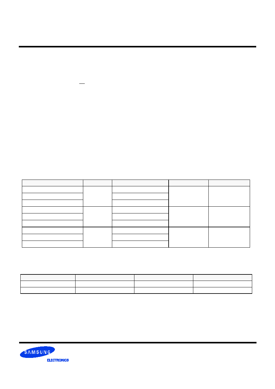
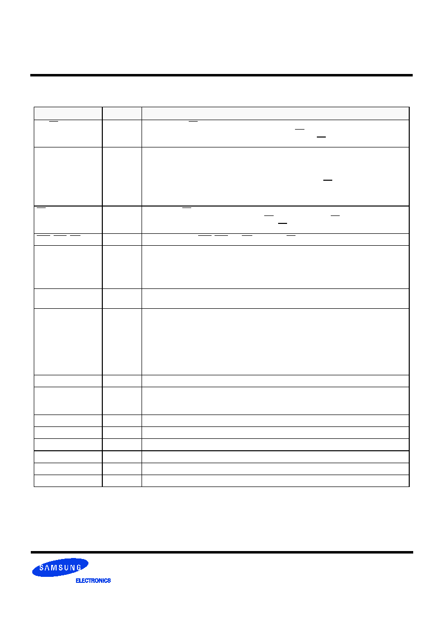
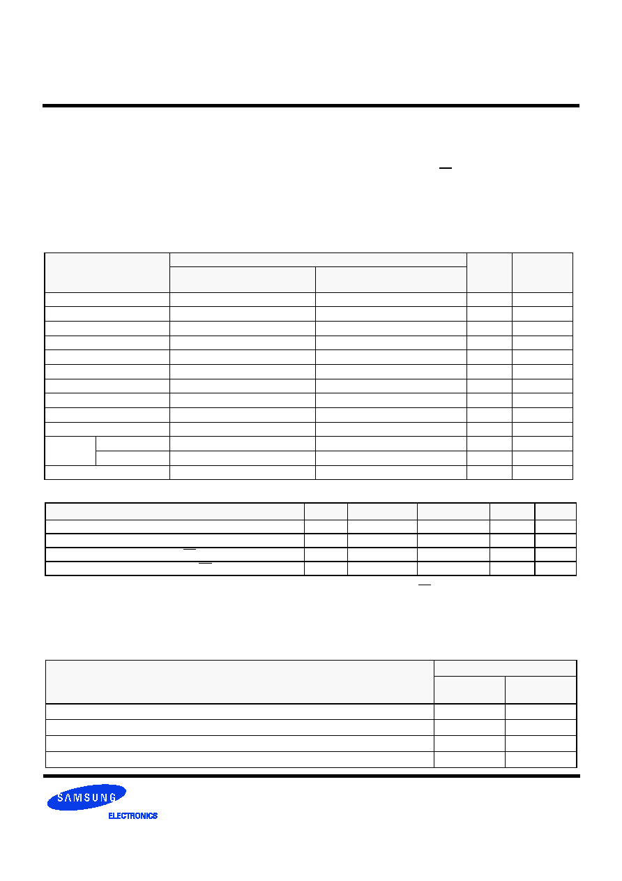
Key Features
Operating Frequencies
*CL : Cas Latency
- B3(DDR333)
- A2(DDR266A)
- B0(DDR266B)
Speed @CL2
133MHz
133MHz
100MHz
Speed @CL2.5
166MHz
133MHz
133MHz
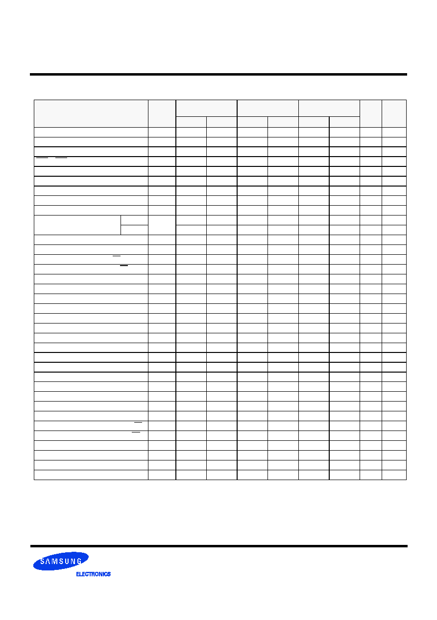
Part No.
Org.
Max Freq.
Interface
Package
K4H560438D-GC(L)B3
64M x 4
B3(DDR333@CL=2.5)
SSTL2
60 ball FBGA
K4H560438D-GC(L)A2
A2(DDR266@CL=2)
K4H560438D-GC(L)B0
B0(DDR266@CL=2.5)
K4H560838D-GC(L)B3
32M x 8
B3(DDR333@CL=2.5)
SSTL2
60 ball FBGA
K4H560838D-GC(L)A2
A2(DDR266@CL=2)
K4H560838D-GC(L)B0
B0(DDR266@CL=2.5)
K4H561638D-GC(L)B3
16M x 16
B3(DDR333@CL=2.5)
SSTL2
60 ball FBGA
K4H561638D-GC(L)A2
A2(DDR266@CL=2)
K4H561638D-GC(L)B0
B0(DDR266@CL=2.5)
ORDERING INFORMATION
- 2 -
256Mb
DDR SDRAM
Rev. 2.2 Mar. '03
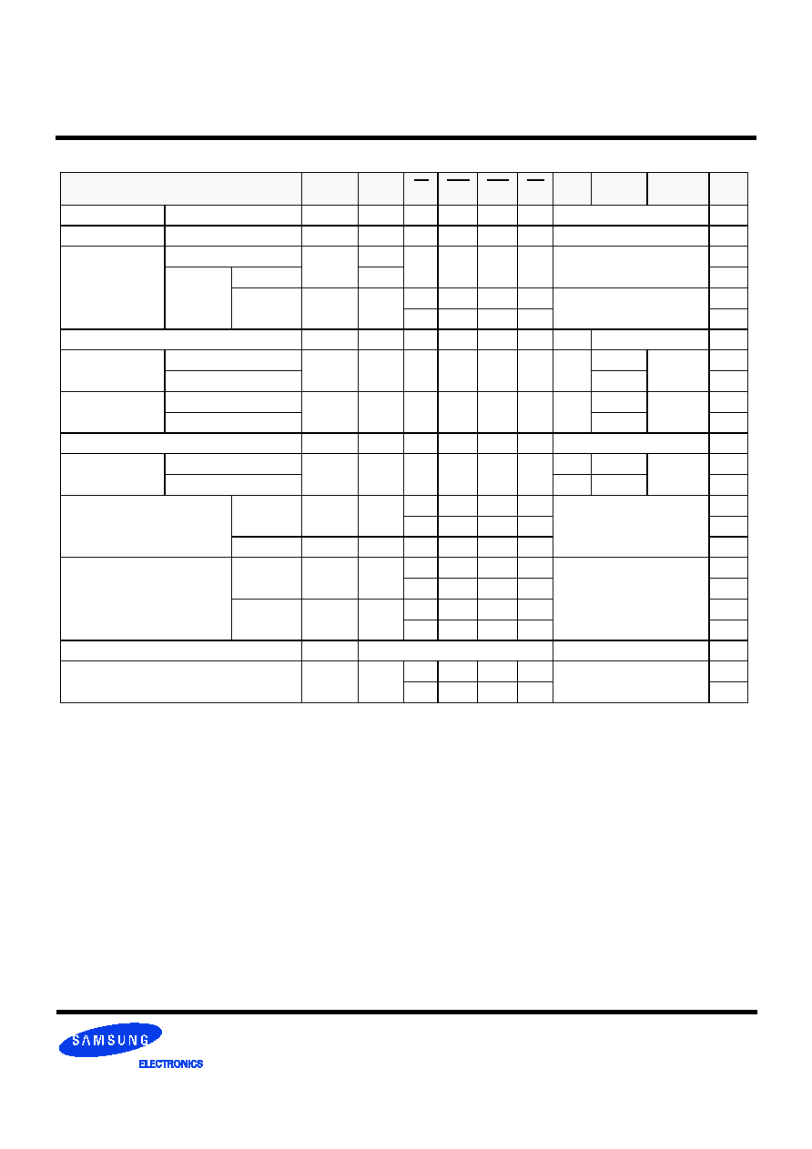
(0.90)
(0.90)
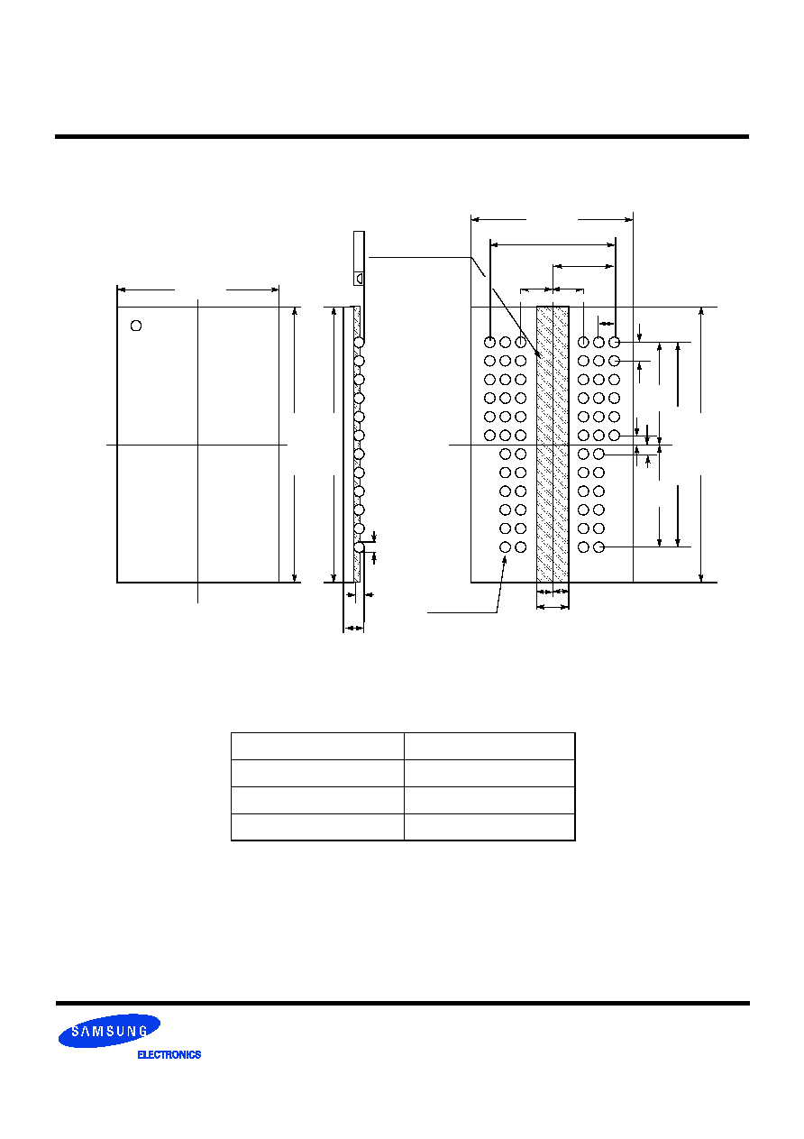
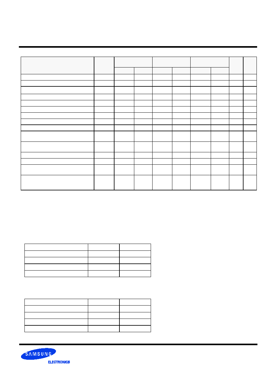
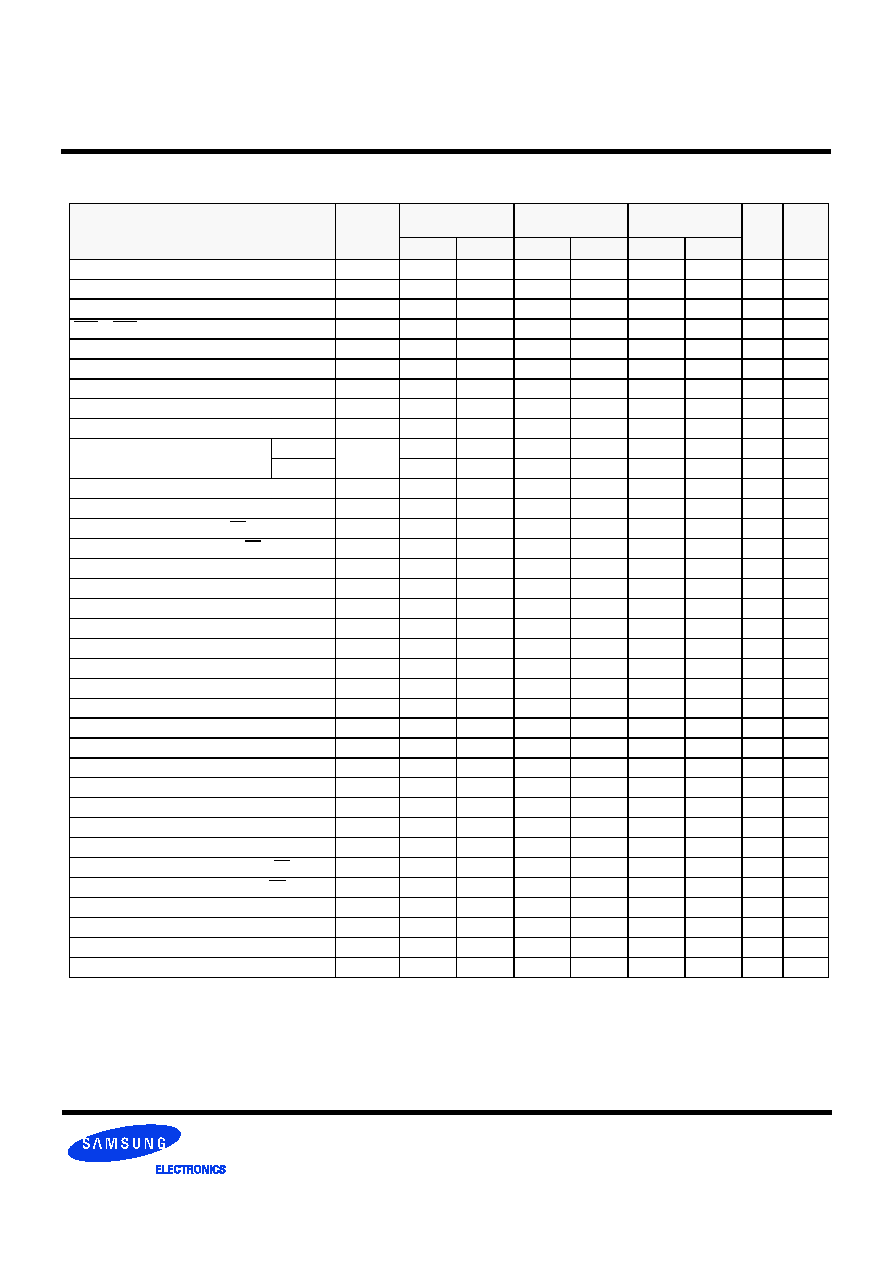
Package Dimension
DM is internally loaded to match DQ and DQS identically.
Column address configuration
Organization
Column Address
64Mx4
A0-A9, A11
32Mx8
A0-A9
16Mx16
A0-A8
8.0 0
±
0.10
14
.
0
0
±
0.
1
0
14
.0
±
0.10
0.
1
0
Ma
x
0.
4
5
±
0.0
5
0.35
±
0.05
1.10
±
0.10
1
2
3
4
5
6
7
8
9
ENCAPSULANT AREA
8.00
±
0.10
0.80 x 4 = 3.20
0.80 x 2 = 1.60
0.80 x 2 = 1.60
A
B
C
D
E
F
G
H
J
K
L
M
0.80
0.
50
5.
5
0
1
.
00
x 11
=
11
.
0
0
14
.
0
0
±
0.
1
0
5.
5
0
60 - 0.45
±
0.05
0.80 x 8 = 6.40
TOP VIEW
BOTTOM VIEW
(1.80)
0.
50
1.0
0
- 3 -
DDR SDRAM
Rev. 2.2 Mar. '03
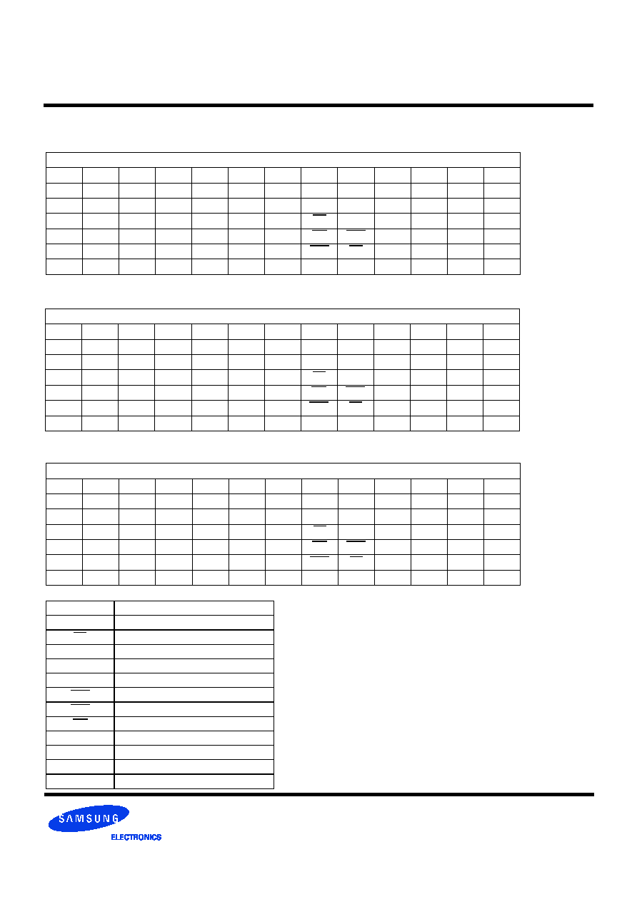
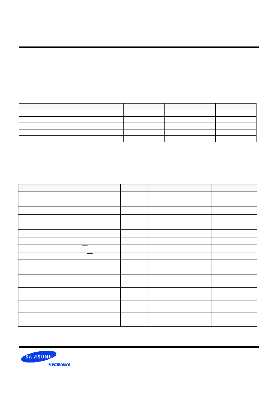
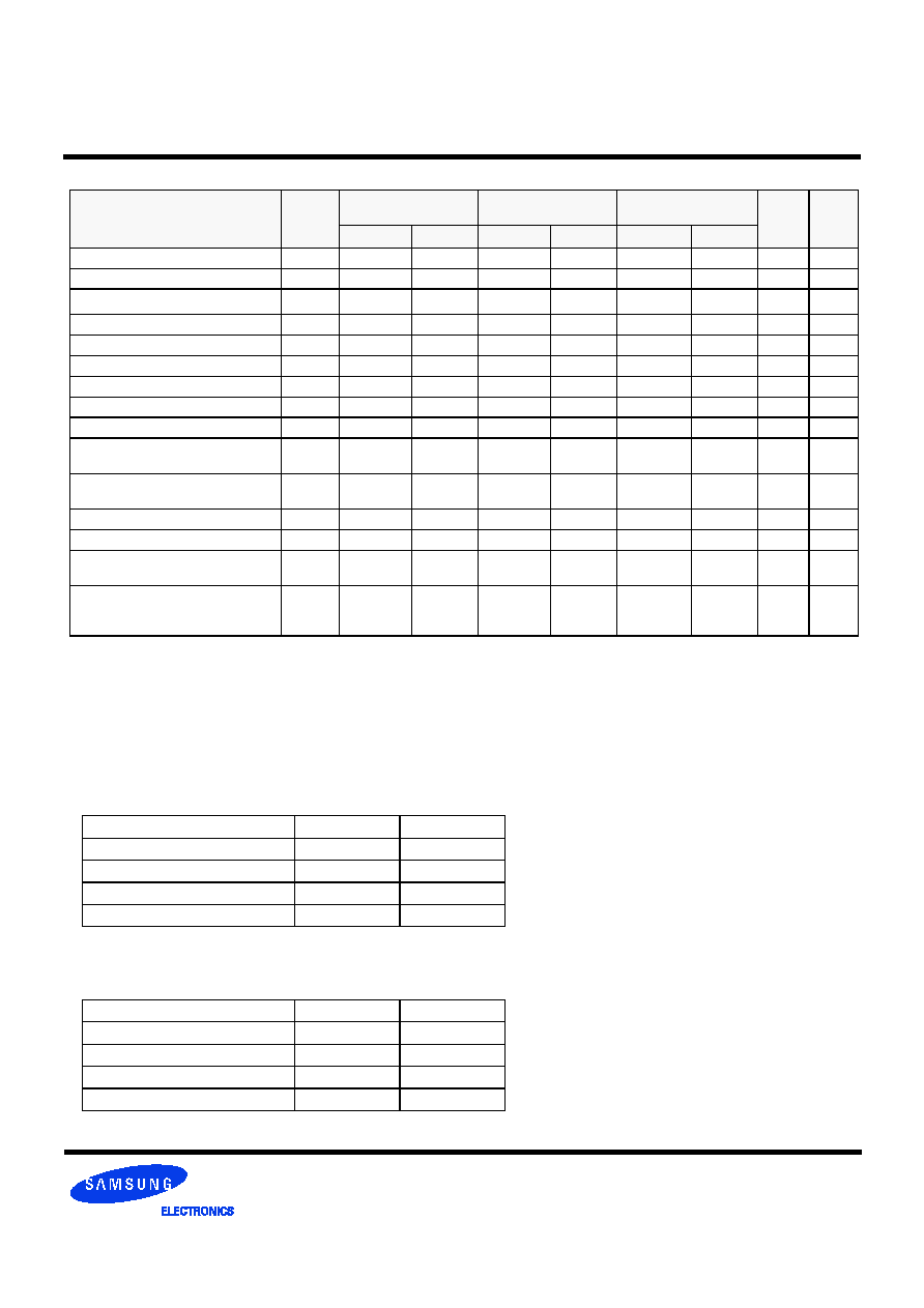
K4H561638D
60Ball CSP
A
B
C
D
E
F
G
H
J
K
L
M
1
VSSQ
NC
NC
NC
NC
VREF
2
NC
VDDQ
VSSQ
VDDQ
VSSQ
VSS
CK
A12
A11
A8
A6
A4
3
VSS
DQ3
NC
DQ2
DQS
DM
CK
CKE
A9
A7
A5
VSS
7
VDD
DQ0
NC
DQ1
NC
NC
WE
RAS
BA1
A0
A2
VDD
8
NC
VSSQ
VDDQ
VSSQ
VDDQ
VDD
CAS
CS
BA0
A10
A1
A3
9
VDDQ
NC
NC
NC
NC
NC
Pin Name
Pin Function
CLK
System Clock
CS
Chip Select
CKE
Clock Enable
A
0
~ A
12
Address
BA
0
~ BA
1
Bank Select Address
RAS
Row Address Strobe
CAS
Column Address Strobe
WE
Write Enable
L(U)DQM
Data Input/Output Mask
DQ
0
~
15
Data Input/Output
V
DD
/V
SS
Power Supply/Ground
V
DDQ
/V
SSQ
Data Output Power/Ground
Pin configuration
60Ball CSP
A
B
C
D
E
F
G
H
J
K
L
M
1
VSSQ
NC
NC
NC
NC
VREF
2
DQ7
VDDQ
VSSQ
VDDQ
VSSQ
VSS
CK
A12
A11
A8
A6
A4
3
VSS
DQ6
DQ5
DQ4
DQS
DM
CK
CKE
A9
A7
A5
VSS
7
VDD
DQ1
DQ2
DQ3
NC
NC
WE
RAS
BA1
A0
A2
VDD
8
DQ0
VSSQ
VDDQ
VSSQ
VDDQ
VDD
CAS
CS
BA0
A10
A1
A3
9
VDDQ
NC
NC
NC
NC
NC
60Ball CSP
A
B
C
D
E
F
G
H
J
K
L
M
1
VSSQ
DQ14
DQ12
DQ10
DQ8
VREF
2
DQ15
VDDQ
VSSQ
VDDQ
VSSQ
VSS
CK
A12
A11
A8
A6
A4
3
VSS
DQ13
DQ11
DQ9
UDQS
UDM
CK
CKE
A9
A7
A5
VSS
7
VDD
DQ2
DQ4
DQ6
LDQS
LDM
WE
RAS
BA1
A0
A2
VDD
8
DQ0
VSSQ
VDDQ
VSSQ
VDDQ
VDD
CAS
CS
BA0
A10
A1
A3
9
VDDQ
DQ1
DQ3
DQ5
DQ7
NC
16M x 16
32M x 8
64M x 4

- 4 -
256Mb
DDR SDRAM
Rev. 2.2 Mar. '03
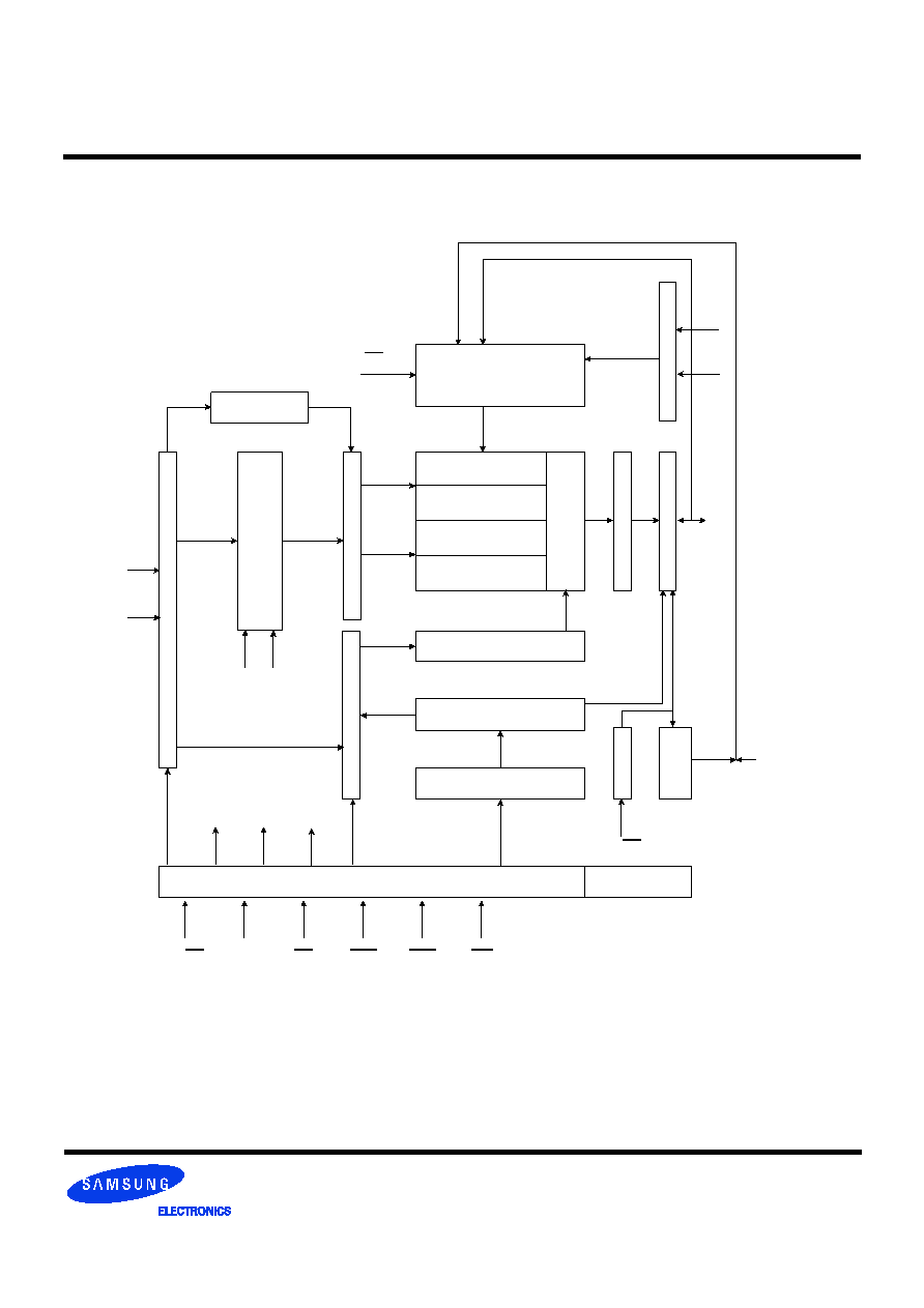
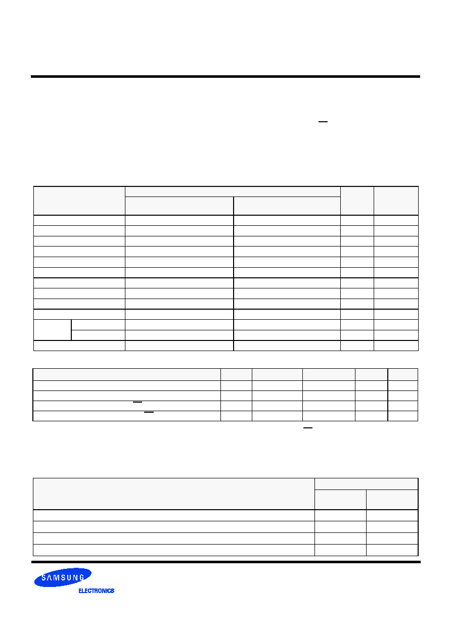
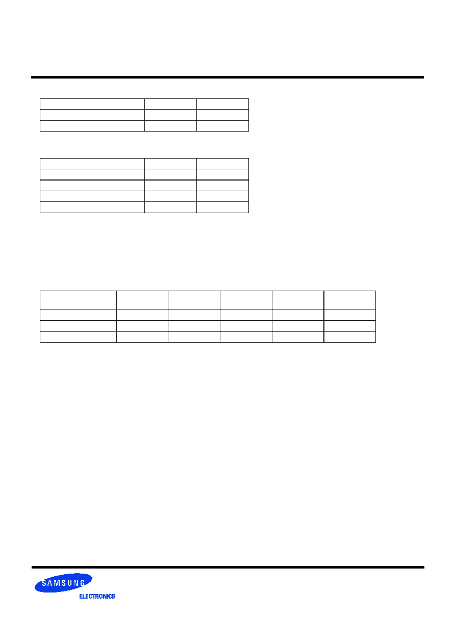
Bank Select
Timing Register
Address Reg
i
ster
Refresh Counter
Row Buf
f
er
Row Decoder
Col
.
Buf
f
er
Data Input Register
Serial to parallel
8Mx8
8Mx8
8Mx8
8Mx8
Sense AMP
2-bit prefetch
Output Buf
f
er
I/O
Cont
rol
Column Decoder
Latency & Burst Length
Programming Register
DLL
St
r
o
b
e
Ge
n.
CK, CK
ADD
LCKE
CK, CK
CKE
CS
RAS
CAS
WE
CK, CK
LCAS
LRAS LCBR
LWE
LWCBR
LRAS
LCBR
CK, CK
8
8
4
4
WE
DM
x4
DQi
Data Strobe
Block Diagram (16Mbit x 4 I/O x 4 Banks)

- 5 -
256Mb
DDR SDRAM
Rev. 2.2 Mar. '03
Bank Select
Timing Register
Address Reg
i
ster
Refresh Counter
Row Buf
f
er
Row Decoder
Col
.
Buf
f
er
Data Input Register
Serial to parallel
4Mx16
4Mx16
4Mx16
4Mx16
Sense AMP
2-bit prefetch
Output Buf
f
er
I/O
Cont
rol
Column Decoder
Latency & Burst Length
Programming Register
DLL
St
r
o
b
e
Ge
n.
CK, CK
ADD
LCKE
CK, CK
CKE
CS
RAS
CAS
WE
CK, CK
LCAS
LRAS LCBR
LWE
LWCBR
LRAS
LCBR
CK, CK
16
16
8
8
WE
DM
x8
DQi
Data Strobe
Block Diagram (8Mbit x 8 I/O x 4 Banks)
- 6 -
256Mb
DDR SDRAM
Rev. 2.2 Mar. '03
Bank Select
Timing Register
Address Reg
i
ster
Refresh Counter
Row Buf
f
er
Row Decoder
Col
.
Buf
f
er
Data Input Register
Serial to parallel
2Mx32
2Mx32
2Mx32
2Mx32
Sense AMP
2-bit prefetch
Output Buf
f
er
I/O
Cont
rol
Column Decoder
Latency & Burst Length
Programming Register
DLL
St
r
o
b
e
Ge
n.
ADD
LCKE
CK, CK
CKE
CS
RAS
CAS
WE
CK, CK
LCAS
LRAS LCBR
LWE
LWCBR
LRAS
LCBR
CK, CK
32
32
16
16
LWE
LDM
x16
DQi
Data Strobe
Block Diagram (4Mbit x 16 I/O x 4 Banks)
- 7 -
256Mb
DDR SDRAM
Rev. 2.2 Mar. '03
Input/Output Function Description
SYMBOL
TYPE
DESCRIPTION
CK, CK
Input
Clock : CK and CK are differential clock inputs. All address and control input signals are sam-
pled on the positive edge of CK and negative edge of CK. Output (read) data is referenced to
both edges of CK. Internal clock signals are derived from CK/CK.
CKE
Input
Clock Enable : CKE HIGH activates, and CKE LOW deactivates internal clock signals, and
device input buffers and output drivers. Deactivating the clock provides PRECHARGE
POWER-DOWN and SELF REFRESH operation (all banks idle), or ACTIVE POWER-DOWN
(row ACTIVE in any bank). CKE is synchronous for all functions except for disabling outputs,
which is achieved asynchronously. Input buffers, excluding CK, CK and CKE are disabled
during power-down and self refresh modes, providing low standby power. CKE will recognize
an LVCMOS LOW level prior to VREF being stable on power-up.
CS
Input
Chip Select : CS enables(registered LOW) and disables(registered HIGH) the command
decoder. All commands are masked when CS is registered HIGH. CS provides for external
bank selection on systems with multiple banks. CS is considered part of the command code.
RAS, CAS, WE
Input
Command Inputs : RAS, CAS and WE (along with CS) define the command being entered.
LDM,(U)DM
Input
Input Data Mask : DM is an input mask signal for write data. Input data is masked when DM is
sampled HIGH along with that input data during a WRITE access. DM is sampled on both
edges of DQS. DM pins include dummy loading internally, to matches the DQ and DQS load-
ing. For the x16, LDM corresponds to the data on DQ0-DQ7 ; UDM correspons to the data on
DQ8-DQ15.
BA0, BA1
Input
Bank Addres Inputs : BA0 and BA1 define to which bank an ACTIVE, READ, WRITE or PRE-
CHARGE command is being applied.
A [n : 0]
Input
Address Inputs : Provide the row address for ACTIVE commands, and the column address
and AUTO PRECHARGE bit for READ/WRITE commands, to select one location out of the
memory array in the respective bank. A10 is sampled during a PRECHARGE command to
determine whether the PRECHARGE applies to one bank (A10 LOW) or all banks (A10
HIGH). If only one bank is to be precharged, the bank is selected by BA0, BA1. The address
inputs also provide the op-code during a MODE REGISTER SET command. BA0 and BA1
define which mode register is loaded during the MODE REGISTER SET command (MRS or
EMRS).
DQ
I/O
Data Input/Output : Data bus
LDQS,(U)DQS
I/O
Data Strobe : Output with read data, input with write data. Edge-aligned with read data, cen-
tered in write data. Used to capture write data. For the x16, LDQS corresponds to the data on
DQ0-DQ7 ; UDQS corresponds to the data on DQ8-DQ15.
NC
-
No Connect : No internal electrical connection is present.
V
DD
Q
Supply
DQ Power Supply : +2.5V
±
0.2V.
V
SS
Q
Supply
DQ Ground.
V
DD
Supply
Power Supply : +2.5V
±
0.2V (device specific).
V
SS
Supply
Ground.
V
REF
Input
SSTL_2 reference voltage.
- 8 -
256Mb
DDR SDRAM
Rev. 2.2 Mar. '03
Command Truth Table
(V=Valid, X=Don
t Care, H=Logic High, L=Logic Low)
COMMAND
CKEn-1
CKEn
CS
RAS
CAS
WE
BA
0,1
A
10
/AP
A
11,
A
12
A
9
~ A
0
Note
Register
Extended MRS
H
X
L
L
L
L
OP CODE
1, 2
Register
Mode Register Set
H
X
L
L
L
L
OP CODE
1, 2
Refresh
Auto Refresh
H
H
L
L
L
H
X
3
Self
Refresh
Entry
L
3
Exit
L
H
L
H
H
H
X
3
H
X
X
X
3
Bank Active & Row Address
H
X
L
L
H
H
V
Row Address
Read &
Column Address
Auto Precharge Disable
H
X
L
H
L
H
V
L
Column
Address
4
Auto Precharge Enable
H
4
Write &
Column Address
Auto Precharge Disable
H
X
L
H
L
L
V
L
Column
Address
4
Auto Precharge Enable
H
4, 6
Burst Stop
H
X
L
H
H
L
X
7
Precharge
Bank Selection
H
X
L
L
H
L
V
L
X
All Banks
X
H
5
Active Power Down
Entry
H
L
H
X
X
X
X
L
V
V
V
Exit
L
H
X
X
X
X
Precharge Power Down Mode
Entry
H
L
H
X
X
X
X
L
H
H
H
Exit
L
H
H
X
X
X
L
V
V
V
DM
H
X
X
8
No operation (NOP) : Not defined
H
X
H
X
X
X
X
9
L
H
H
H
9
1. OP Code : Operand Code. A
0
~ A
12
& BA
0
~ BA
1
: Program keys. (@EMRS/MRS)
2.EMRS/ MRS can be issued only at all banks precharge state.
A new command can be issued 2 clock cycles after EMRS or MRS.
3. Auto refresh functions are same as the CBR refresh of DRAM.
The automatical precharge without row precharge command is meant by "Auto".
Auto/self refresh can be issued only at all banks precharge state.
4. BA
0
~ BA
1
: Bank select addresses.
If both BA
0
and BA
1
are "Low" at read, write, row active and precharge, bank A is selected.
If BA
0
is "High" and BA
1
is "Low" at read, write, row active and precharge, bank B is selected.
If BA
0
is "Low" and BA
1
is "High" at read, write, row active and precharge, bank C is selected.
If both BA
0
and BA
1
are "High" at read, write, row active and precharge, bank D is selected.
5. If A
10
/AP is "High" at row precharge, BA
0
and BA
1
are ignored and all banks are selected.
6. During burst write with auto precharge, new read/write command can not be issued.
Another bank read/write command can be issued after the end of burst.
New row active of the associated bank can be issued at t
RP
after the end of burst.
7. Burst stop command is valid at every burst length.
8. DM sampled at the rising and falling edges of the DQS and Data-in are masked at the both edges (Write DM latency is 0).
9. This combination is not defined for any function, which means "No Operation(NOP)" in DDR SDRAM.
- 9 -
K4H560438D
DDR SDRAM
Rev. 2.2 Mar. '03
16M x 4Bit x 4 Banks Double Data Rate SDRAM
Absolute Maximum Rating
Parameter
Symbol
Value
Unit
Voltage on any pin relative to VSS
VIN, VOUT
-0.5 ~ 3.6
V
Voltage on VDD & VDDQ supply relative to VSS
VDD, VDDQ
-1.0 ~ 3.6
V
Storage temperature
TSTG
-55 ~ +150
∞
C
Power dissipation
PD
1.5
W
Short circuit current
IOS
50
mA
Note : Permanent device damage may occur if ABSOLUTE MAXIMUM RATINGS are exceeded.
Functional operation should be restricted to recommend operation condition.
Exposure to higher than recommended voltage for extended periods of time could affect device reliability
DC Operating Conditions
The K4H560438D is 268,435,456 bits of double data rate synchronous DRAM organized as 4 x 16,777,216 words by 4 bits, fabricated
with SAMSUNG
s high performance CMOS technology. Synchronous features with Data Strobe allow extremely high performance up to
333Mb/s per pin. I/O transactions are possible on both edges of DQS. Range of operating frequencies, programmable burst length and
programmable latencies allow the device to be useful for a variety of high performance memory system applications.
GENERAL DESCRIPTION
Recommended operating conditions(Voltage referenced to V
SS
=0V, T
A
= 0 to 70
∞
C)
Parameter
Symbol
Min
Max
Unit
Note
Supply voltage(for device with a nominal V
DD
of 2.5V)
V
DD
2.3
2.7
I/O Supply voltage
V
DDQ
2.3
2.7
V
I/O Reference voltage
V
REF
VDDQ/2-50mV
VDDQ/2+50mV
V
1
I/O Termination voltage(system)
V
TT
V
REF
-0.04
V
REF
+0.04
V
2
Input logic high voltage
V
IH
(DC)
V
REF
+0.15
V
DDQ
+0.3
V
4
Input logic low voltage
V
IL
(DC)
-0.3
V
REF
-0.15
V
4
Input Voltage Level, CK and CK inputs
V
IN
(DC)
-0.3
V
DDQ
+0.3
V
Input Differential Voltage, CK and CK inputs
V
ID
(DC)
0.3
V
DDQ
+0.6
V
3
Input crossing point voltage, CK and CK inputs
V
IX
(DC)
1.15
1.35
V
5
Input leakage current
I
I
-2
2
uA
Output leakage current
I
OZ
-5
5
uA
Output High Current(Normal strengh driver)
;V
OUT
= V
TT
+ 0.84V
I
OH
-16.8
mA
Output High Current(Normal strengh driver)
;V
OUT
= V
TT
- 0.84V
I
OL
16.8
mA
Output High Current(Half strengh driver)
;V
OUT
=
V
TT
+ 0.45V
I
OH
-9
mA
Output High Current(Half strengh driver)
;V
OUT
= V
TT
- 0.45V
I
OL
9
mA
- 10 -
K4H560438D
DDR SDRAM
Rev. 2.2 Mar. '03
Notes 1. Includes
±
25mV margin for DC offset on V
REF
, and a combined total of
±
50mV margin for all AC noise and DC offset on
V
REF
, bandwidth limited to 20MHz. The DRAM must accommodate DRAM current spikes on V
REF
and internal DRAM noise
coupled TO V
REF
, both of which may result in V
REF
noise. V
REF
should be de-coupled with an inductance of
3nH.
2. V
TT
is not applied directly to the device. V
TT
is a system supply for signal termination resistors, is expected to be set equal to
V
REF
, and must track variations in the DC level of V
REF
3. V
ID
is the magnitude of the difference between the input level on CK and the input level on CK.
4. These parameters should be tested at the pin on actual components and may be checked at either the pin or the pad in
simulation. The AC and DC input specifications are relative to a VREF envelop that has been bandwidth limited to 200MHZ.
5. The value of V
IX
is expected to equal 0.5*V
DDQ
of the transmitting device and must track variations in the dc level of the same.
DDR SDRAM IDD spec table
AC Operating Conditions
Parameter/Condition
Symbol
Min
Max
Unit
Note
Input High (Logic 1) Voltage, DQ, DQS and DM signals
VIH(AC)
VREF + 0.31
V
3
Input Low (Logic 0) Voltage, DQ, DQS and DM signals.
VIL(AC)
VREF - 0.31
V
3
Input Differential Voltage, CK and CK inputs
VID(AC)
0.7
VDDQ+0.6
V
1
Input Crossing Point Voltage, CK and CK inputs
VIX(AC)
0.5*VDDQ-0.2
0.5*VDDQ+0.2
V
2
Note 1. VID is the magnitude of the difference between the input level on CK and the input on CK.
2. The value of V
IX
is expected to equal 0.5*V
DDQ
of the transmitting device and must track variations in the DC level of the same.
3. These parameters should be tested at the pim on actual components and may be checked at either the pin or the pad in simu
lation. the AC and DC input specificatims are refation to a Vref envelope that has been bandwidth limited 20MHz.
(V
DD
=2.7V, T
= 10
∞
C
)
Parameter
Specification
Address &
Control pins
Data pins
Maximum peak amplitude allowed for overshoot
1.6 V
1.2V
Maximum peak amplitude allowed for undershoot
1.6 V
1.2V
The area between the overshoot signal and VDD must be less than or equal to
4.5 V-ns
2.5 V-ns
The area between the undershoot signal and GND must be less than or equal to
4.5 V-ns
2.5 V-ns
Overshoot/Undershoot specification
Symbol
64Mx4
Unit
Notes
K4H560438D-GC(L)B3
(DDR333)
K4H560438D-GC(L)A2,B0
(DDR266A/B)
IDD0
90
80
mA
IDD1
110
100
mA
IDD2P
3
3
mA
IDD2F
25
20
mA
IDD2Q
20
18
mA
IDD3P
35
30
mA
IDD3N
55
45
mA
IDD4R
150
120
mA
IDD4W
160
135
mA
IDD5
180
165
mA
IDD6
Normal
3
3
mA
Low power
1.5
1.5
mA
Optional
IDD7A
290
250
mA
- 11 -
K4H560438D
DDR SDRAM
Rev. 2.2 Mar. '03
AC Timming Parameters & Specifications
Parameter
Symbol
B3
(DDR333)
A2
(DDR266A)
B0
(DDR266B)
Unit
Note
Min
Max
Min
Max
Min
Max
Row cycle time
tRC
60
65
65
ns
Refresh row cycle time
tRFC
72
75
75
ns
Row active time
tRAS
42
70K
45
120K
45
120K
ns
RAS to CAS delay
tRCD
18
20
20
ns
Row precharge time
tRP
18
20
20
ns
Row active to Row active delay
tRRD
12
15
15
ns
Write recovery time
tWR
15
15
15
ns
Last data in to Read command
tWTR
1
1
1
tCK
Col. address to Col. address delay
tCCD
1
1
1
tCK
Clock cycle time
CL=2.0
tCK
7.5
12
7.5
12
10
12
ns
5
CL=2.5
6
12
7.5
12
7.5
12
ns
5
Clock high level width
tCH
0.45
0.55
0.45
0.55
0.45
0.55
tCK
Clock low level width
tCL
0.45
0.55
0.45
0.55
0.45
0.55
tCK
DQS-out access time from CK/CK
tDQSCK
-0.6
+0.6
-0.75
+0.75
-0.75
+0.75
ns
Output data access time from CK/CK
tAC
-0.7
+0.7
-0.75
+0.75
-0.75
+0.75
ns
Data strobe edge to ouput data edge
tDQSQ
-
0.4
-
0.5
-
0.5
ns
5
Read Preamble
tRPRE
0.9
1.1
0.9
1.1
0.9
1.1
tCK
Read Postamble
tRPST
0.4
0.6
0.4
0.6
0.4
0.6
tCK
CK to valid DQS-in
tDQSS
0.75
1.25
0.75
1.25
0.75
1.25
tCK
DQS-in setup time
tWPRES
0
0
0
ns
2
DQS-in hold time
tWPRE
0.25
0.25
0.25
tCK
DQS falling edge to CK rising-setup time
tDSS
0.2
0.2
0.2
tCK
DQS falling edge from CK rising-hold time
tDSH
0.2
0.2
0.2
tCK
DQS-in high level width
tDQSH
0.35
0.35
0.35
tCK
DQS-in low level width
tDQSL
0.35
0.35
0.35
tCK
DQS-in cycle time
tDSC
0.9
1.1
0.9
1.1
0.9
1.1
tCK
Address and Control Input setup time(fast)
tIS
0.75
0.9
0.9
ns
6
Address and Control Input hold time(fast)
tIH
0.75
0.9
0.9
ns
6
Address and Control Input setup time(slow)
tIS
0.8
1.0
1.0
ns
6
Address and Control Input hold time(slow)
tIH
0.8
1.0
1.0
ns
6
Data-out high impedence time from CK/CK
tHZ
-0.7
+0.7
-0.75
+0.75
-0.75
+0.75
ns
Data-out low impedence time from CK/CK
tLZ
-0.7
+0.7
-0.75
+0.75
-0.75
+0.75
ns
Input Slew Rate(for input only pins)
tSL(I)
0.5
0.5
0.5
V/ns
6
Input Slew Rate(for I/O pins)
tSL(IO)
0.5
0.5
0.5
V/ns
7
Output Slew Rate(x4,x8)
tSL(O)
1.0
4.5
1.0
4.5
1.0
4.5
V/ns
10
Output Slew Rate Matching Ratio(rise to fall)
tSLMR
0.67
1.5
0.67
1.5
0.67
1.5
- 12 -
K4H560438D
DDR SDRAM
Rev. 2.2 Mar. '03
1. Maximum burst refresh cycle : 8
2. The specific requirement is that DQS be valid(High or Low) on or before this CK edge. The case shown(DQS going from
High_Z to logic Low) applies when no writes were previously in progress on the bus. If a previous write was in progress,
DQS could be High at this time, depending on tDQSS.
3. The maximum limit for this parameter is not a device limit. The device will operate with a great value for this parameter,
but system performance (bus turnaround) will degrade accordingly.
4. A write command can be applied with t
RCD
satisfied after this command.
5. For registered DIMMs, t
CL
and t
CH
are
45% of the period including both the half period jitter (t
JIT(HP)
) of the PLL and the half period
jitter due to crosstalk (t
JIT
(crosstalk)
) on the DIMM.
6. Input Setup/Hold Slew Rate Derating
This derating table is used to increase t
IS
/t
IH
in the case where the input slew rate is below 0.5V/ns. Input setup/hold slew rate
based on the lesser of AC-AC slew rate and DC-DC slew rate.
7. I/O Setup/Hold Slew Rate Derating
This derating table is used to increase t
DS
/t
DH
in the case where the I/O slew rate is below 0.5V/ns. I/O setup/hold slew rate
based on the lesser of AC-AC slew rate and DC-DC slew rate.
Parameter
Symbol
-GC(L)B3
(DDR333)
-GC(L)A2
(DDR266A)
-GC(L)B0
(DDR266B)
Unit
Note
Min
Max
Min
Max
Min
Max
Mode register set cycle time
tMRD
12
15
15
ns
DQ & DM setup time to DQS
tDS
0.45
0.5
0.5
ns
7,8,9
DQ & DM hold time to DQS
tDH
0.45
0.5
0.5
ns
7,8,9
Control & Address input pulse width
tIPW
2.2
2.2
2.2
ns
DQ & DM input pulse width
tDIPW
1.75
1.75
1.75
ns
Power down exit time
tPDEX
6
7.5
7.5
ns
Exit self refresh to non-Read command
tXSNR
75
75
75
ns
4
Exit self refresh to read command
tXSRD
200
200
200
tCK
Refresh interval time
tREFI
7.8
7.8
7.8
us
1
Output DQS valid window
tQH
tHP
-tQHS
-
tHP
-tQHS
-
tHP
-tQHS
-
ns
5
Clock half period
tHP
tCLmin
or tCHmin
-
tCLmin
or tCHmin
-
tCLmin
or tCHmin
-
ns
Data hold skew factor
tQHS
0.5
0.75
0.75
ns
DQS write postamble time
tWPST
0.4
0.6
0.4
0.6
0.4
0.6
tCK
3
Active to Read with Auto precharge
command
tRAP
18 20
20
Autoprecharge write recovery +
Precharge time
tDAL
(tWR/tCK)
+
(tRP/tCK)
(tWR/tCK)
+
(tRP/tCK)
(tWR/tCK)
+
(tRP/tCK)
tCK
11
Input Setup/Hold Slew Rate
tIS
tIH
(V/ns)
(ps)
(ps)
0.5
0
0
0.4
+50
+50
0.3
+100
+100
I/O Setup/Hold Slew Rate
tDS
tDH
(V/ns)
(ps)
(ps)
0.5
0
0
0.4
+75
+75
0.3
+150
+150

- 13 -
K4H560438D
DDR SDRAM
Rev. 2.2 Mar. '03
8. I/O Setup/Hold Plateau Derating
This derating table is used to increase tDS/tDH in the case where the input level is flat below VREF
±
310mV for a duration of
up to 2ns.
9. I/O Delta Rise/Fall Rate(1/slew-rate) Derating
This derating table is used to increase t
DS
/t
DH
in the case where the DQ and DQS slew rates differ. The Delta Rise/Fall Rate
is calated as 1/SlewRate1-1/SlewRate2. For example, if slew rate 1 = 5V/ns and slew rate 2 =.4V/ns then the Delta Rise/Fall
Rate =-0/5ns/V. Input S/H slew rate based on larger of AC-AC delta rise/fall rate and DC-DC delta rise/fall rate.
10. This parameter is fir system simulation purpose. It is guranteed by design.
11. For each of the terms, if not already an integer, round to the next highest integer. tCK is actual to the system clock cycle time.
I/O Input Level
tDS
tDH
(mV)
(ps)
(ps)
±
280
+50
+50
Delta Rise/Fall Rate
tDS
tDH
(ns/V)
(ps)
(ps)
0
0
0
±
0.25
+50
+50
±
0.5
+100
+100
The following table specifies derating values for the specifications listed if the single-ended clock skew rate is less than 1.0V/ns.
CK slew rate
(Single ended)
tIH/tIS
(ps)
tDSS/tDSH
(ps)
tAC/tDQSCK
(ps)
tLZ(min)
(ps)
tHZ(max)
(ps)
1.0V/ns
0
0
0
0
0
0.75V/ns
+50
+50
+50
-50
+50
0.5V/ns
+100
+100
+100
-100
+100
<Reference>
- 14 -
K4H560438D
DDR SDRAM
Rev. 2.2 Mar. '03
AC Operating Test Conditions
Input/Output Capacitance
(VDD=2.5, VDDQ=2.5V, TA= 25
∞
C, f=1MHz)
Parameter
Symbol
Min
Max
Delta Cap(max)
Unit
Input capacitance
(A0 ~ A12, BA0 ~ BA1, CKE, CS, RAS,CAS, WE)
CIN1
1.5
3.5
0.5
pF
Input capacitance( CK, CK )
CIN2
1.5
3.5
0.25
pF
Data & DQS input/output capacitance
COUT
3.5
5.5
0.5
pF
Input capacitance(DM)
CIN3
3.5
5.5
pF
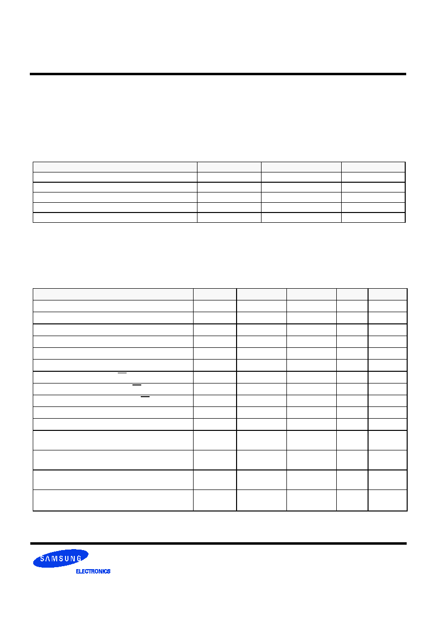
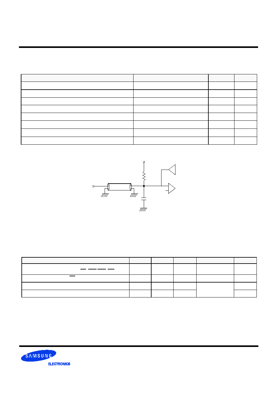
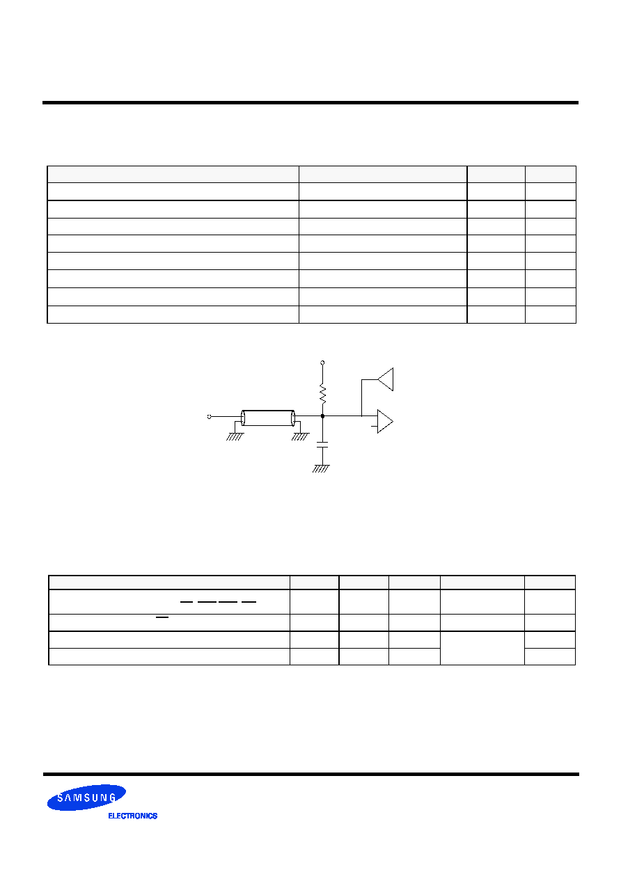
Output Load Circuit (SSTL_2)
Output
Z0=50
C
LOAD
=30pF
V
REF
=0.5*V
DDQ
R
T
=50
V
tt
=0.5*V
DDQ
(V
DD
=2.5V, V
DDQ
=2.5V, T
A
= 0 to 70
∞
C)
Parameter
Value
Unit
Note
Input reference voltage for Clock
0.5 * V
DDQ
V
Input signal maximum peak swing
1.5
V
Input signal minimum slew rate (for imput only)
0.5
V/ns
Input slew rate (I/O pins)
0.5
V/ns
Input Levels(V
IH
/V
IL
)
V
REF
+0.31/V
REF
-0.31
V
Input timing measurement reference level
V
REF
V
Output timing measurement reference level
V
tt
V
Output load condition
See Load Circuit
- 15 -
K4H560838D
DDR SDRAM
Rev. 2.2 Mar. '03
8M x 8Bit x 4 Banks Double Data Rate SDRAM
Absolute Maximum Rating
Parameter
Symbol
Value
Unit
Voltage on any pin relative to VSS
VIN, VOUT
-0.5 ~ 3.6
V
Voltage on VDD & VDDQ supply relative to VSS
VDD, VDDQ
-1.0 ~ 3.6
V
Storage temperature
TSTG
-55 ~ +150
∞
C
Power dissipation
PD
1.5
W
Short circuit current
IOS
50
mA
Note : Permanent device damage may occur if ABSOLUTE MAXIMUM RATINGS are exceeded.
Functional operation should be restricted to recommend operation condition.
Exposure to higher than recommended voltage for extended periods of time could affect device reliability
DC Operating Conditions
The K4H560838D is 268,435,456 bits of double data rate synchronous DRAM organized as 4 x 8,388,608 words by 8 bits, fabricated
with SAMSUNG
s high performance CMOS technology. Synchronous features with Data Strobe allow extremely high performance up
to 333Mb/s per pin. I/O transactions are possible on both edges of DQS. Range of operating frequencies, programmable burst length
and programmable latencies allow the device to be useful for a variety of high performance memory system applications.
GENERAL DESCRIPTION
Recommended operating conditions(Voltage referenced to V
SS
=0V, T
A
= 0 to 70
∞
C)
Parameter
Symbol
Min
Max
Unit
Note
Supply voltage(for device with a nominal V
DD
of 2.5V)
V
DD
2.3
2.7
I/O Supply voltage
V
DDQ
2.3
2.7
V
I/O Reference voltage
V
REF
VDDQ/2-50mV
VDDQ/2+50mV
V
1
I/O Termination voltage(system)
V
TT
V
REF
-0.04
V
REF
+0.04
V
2
Input logic high voltage
V
IH
(DC)
V
REF
+0.15
V
DDQ
+0.3
V
4
Input logic low voltage
V
IL
(DC)
-0.3
V
REF
-0.15
V
4
Input Voltage Level, CK and CK inputs
V
IN
(DC)
-0.3
V
DDQ
+0.3
V
Input Differential Voltage, CK and CK inputs
V
ID
(DC)
0.3
V
DDQ
+0.6
V
3
Input crossing point voltage, CK and CK inputs
V
IX
(DC)
1.15
1.35
V
5
Input leakage current
I
I
-2
2
uA
Output leakage current
I
OZ
-5
5
uA
Output High Current(Normal strengh driver)
;V
OUT
= V
TT
+ 0.84V
I
OH
-16.8
mA
Output High Current(Normal strengh driver)
;V
OUT
= V
TT
- 0.84V
I
OL
16.8
mA
Output High Current(Half strengh driver)
;V
OUT
=
V
TT
+ 0.45V
I
OH
-9
mA
Output High Current(Half strengh driver)
;V
OUT
= V
TT
- 0.45V
I
OL
9
mA
- 16 -
K4H560838D
DDR SDRAM
Rev. 2.2 Mar. '03
Notes 1. Includes
±
25mV margin for DC offset on V
REF
, and a combined total of
±
50mV margin for all AC noise and DC offset on
V
REF
, bandwidth limited to 20MHz. The DRAM must accommodate DRAM current spikes on V
REF
and internal DRAM noise
coupled TO V
REF
, both of which may result in V
REF
noise. V
REF
should be de-coupled with an inductance of
3nH.
2. V
TT
is not applied directly to the device. V
TT
is a system supply for signal termination resistors, is expected to be set equal to
V
REF
, and must track variations in the DC level of V
REF
3. V
ID
is the magnitude of the difference between the input level on CK and the input level on CK.
4. These parameters should be tested at the pin on actual components and may be checked at either the pin or the pad in
simulation. The AC and DC input specifications are relative to a VREF envelop that has been bandwidth limited to 200MHZ.
5. The value of V
IX
is expected to equal 0.5*V
DDQ
of the transmitting device and must track variations in the dc level of the same.
DDR SDRAM IDD spec table
AC Operating Conditions
Parameter/Condition
Symbol
Min
Max
Unit
Note
Input High (Logic 1) Voltage, DQ, DQS and DM signals
VIH(AC)
VREF + 0.31
V
3
Input Low (Logic 0) Voltage, DQ, DQS and DM signals.
VIL(AC)
VREF - 0.31
V
3
Input Differential Voltage, CK and CK inputs
VID(AC)
0.7
VDDQ+0.6
V
1
Input Crossing Point Voltage, CK and CK inputs
VIX(AC)
0.5*VDDQ-0.2
0.5*VDDQ+0.2
V
2
Note 1. VID is the magnitude of the difference between the input level on CK and the input on CK.
2. The value of V
IX
is expected to equal 0.5*V
DDQ
of the transmitting device and must track variations in the DC level of the same.
3. These parameters should be tested at the pim on actual components and may be checked at either the pin or the pad in simu
lation. the AC and DC input specificatims are refation to a Vref envelope that has been bandwidth limited 20MHz.
(V
DD
=2.7V, T
= 10
∞
C
)
Parameter
Specification
Address &
Control pins
Data pins
Maximum peak amplitude allowed for overshoot
1.6 V
1.2V
Maximum peak amplitude allowed for undershoot
1.6 V
1.2V
The area between the overshoot signal and VDD must be less than or equal to
4.5 V-ns
2.5 V-ns
The area between the undershoot signal and GND must be less than or equal to
4.5 V-ns
2.5 V-ns
Overshoot/Undershoot specification
Symbol
32Mx8
Unit
Notes
K4H560838D-GC(L)B3
(DDR333)
K4H560838D-GC(L)A2, B0
(DDR266A/B)
IDD0
90
80
mA
IDD1
120
110
mA
IDD2P
3
3
mA
IDD2F
25
20
mA
IDD2Q
20
18
mA
IDD3P
35
30
mA
IDD3N
55
45
mA
IDD4R
170
140
mA
IDD4W
170
140
mA
IDD5
180
165
mA
IDD6
Normal
3
3
mA
Low power
1.5
1.5
mA
Optional
IDD7A
325
280
mA
- 17 -
K4H560838D
DDR SDRAM
Rev. 2.2 Mar. '03
AC Timming Parameters & Specifications
Parameter
Symbol
B3
(DDR333)
A2
(DDR266A)
B0
(DDR266B)
Unit
Note
Min
Max
Min
Max
Min
Max
Row cycle time
tRC
60
65
65
ns
Refresh row cycle time
tRFC
72
75
75
ns
Row active time
tRAS
42
70K
45
120K
45
120K
ns
RAS to CAS delay
tRCD
18
20
20
ns
Row precharge time
tRP
18
20
20
ns
Row active to Row active delay
tRRD
12
15
15
ns
Write recovery time
tWR
15
15
15
ns
Last data in to Read command
tWTR
1
1
1
tCK
Col. address to Col. address delay
tCCD
1
1
1
tCK
Clock cycle time
CL=2.0
tCK
7.5
12
7.5
12
10
12
ns
5
CL=2.5
6
12
7.5
12
7.5
12
ns
5
Clock high level width
tCH
0.45
0.55
0.45
0.55
0.45
0.55
tCK
Clock low level width
tCL
0.45
0.55
0.45
0.55
0.45
0.55
tCK
DQS-out access time from CK/CK
tDQSCK
-0.6
+0.6
-0.75
+0.75
-0.75
+0.75
ns
Output data access time from CK/CK
tAC
-0.7
+0.7
-0.75
+0.75
-0.75
+0.75
ns
Data strobe edge to ouput data edge
tDQSQ
-
0.4
-
0.5
-
0.5
ns
5
Read Preamble
tRPRE
0.9
1.1
0.9
1.1
0.9
1.1
tCK
Read Postamble
tRPST
0.4
0.6
0.4
0.6
0.4
0.6
tCK
CK to valid DQS-in
tDQSS
0.75
1.25
0.75
1.25
0.75
1.25
tCK
DQS-in setup time
tWPRES
0
0
0
ns
2
DQS-in hold time
tWPRE
0.25
0.25
0.25
tCK
DQS falling edge to CK rising-setup time
tDSS
0.2
0.2
0.2
tCK
DQS falling edge from CK rising-hold time
tDSH
0.2
0.2
0.2
tCK
DQS-in high level width
tDQSH
0.35
0.35
0.35
tCK
DQS-in low level width
tDQSL
0.35
0.35
0.35
tCK
DQS-in cycle time
tDSC
0.9
1.1
0.9
1.1
0.9
1.1
tCK
Address and Control Input setup time(fast)
tIS
0.75
0.9
0.9
ns
6
Address and Control Input hold time(fast)
tIH
0.75
0.9
0.9
ns
6
Address and Control Input setup time(slow)
tIS
0.8
1.0
1.0
ns
6
Address and Control Input hold time(slow)
tIH
0.8
1.0
1.0
ns
6
Data-out high impedence time from CK/CK
tHZ
-0.7
+0.7
-0.75
+0.75
-0.75
+0.75
ns
Data-out low impedence time from CK/CK
tLZ
-0.7
+0.7
-0.75
+0.75
-0.75
+0.75
ns
Input Slew Rate(for input only pins)
tSL(I)
0.5
0.5
0.5
V/ns
6
Input Slew Rate(for I/O pins)
tSL(IO)
0.5
0.5
0.5
V/ns
7
Output Slew Rate(x4,x8)
tSL(O)
1.0
4.5
1.0
4.5
1.0
4.5
V/ns
10
Output Slew Rate Matching Ratio(rise to fall)
tSLMR
0.67
1.5
0.67
1.5
0.67
1.5
- 18 -
K4H560838D
DDR SDRAM
Rev. 2.2 Mar. '03
1. Maximum burst refresh cycle : 8
2. The specific requirement is that DQS be valid(High or Low) on or before this CK edge. The case shown(DQS going from
High_Z to logic Low) applies when no writes were previously in progress on the bus. If a previous write was in progress,
DQS could be High at this time, depending on tDQSS.
3. The maximum limit for this parameter is not a device limit. The device will operate with a great value for this parameter,
but system performance (bus turnaround) will degrade accordingly.
4. A write command can be applied with t
RCD
satisfied after this command.
5. For registered DIMMs, t
CL
and t
CH
are
45% of the period including both the half period jitter (t
JIT(HP)
) of the PLL and the half period
jitter due to crosstalk (t
JIT
(crosstalk)
) on the DIMM.
6. Input Setup/Hold Slew Rate Derating
This derating table is used to increase t
IS
/t
IH
in the case where the input slew rate is below 0.5V/ns. Input setup/hold slew rate
based on the lesser of AC-AC slew rate and DC-DC slew rate.
7. I/O Setup/Hold Slew Rate Derating
This derating table is used to increase t
DS
/t
DH
in the case where the I/O slew rate is below 0.5V/ns. I/O setup/hold slew rate
based on the lesser of AC-AC slew rate and DC-DC slew rate.
Parameter
Symbol
B3
(DDR333)
A2
(DDR266A)
B0
(DDR266B)
Unit
Note
Min
Max
Min
Max
Min
Max
Mode register set cycle time
tMRD
12
15
15
ns
DQ & DM setup time to DQS
tDS
0.45
0.5
0.5
ns
7,8,9
DQ & DM hold time to DQS
tDH
0.45
0.5
0.5
ns
7,8,9
Control & Address input pulse width
tIPW
2.2
2.2
2.2
ns
DQ & DM input pulse width
tDIPW
1.75
1.75
1.75
ns
Power down exit time
tPDEX
6
7.5
7.5
ns
Exit self refresh to non-Read command
tXSNR
75
75
75
ns
4
Exit self refresh to read command
tXSRD
200
200
200
tCK
Refresh interval time
tREFI
7.8
7.8
7.8
us
1
Output DQS valid window
tQH
tHP
-tQHS
-
tHP
-tQHS
-
tHP
-tQHS
-
ns
5
Clock half period
tHP
tCLmin
or tCHmin
-
tCLmin
or tCHmin
-
tCLmin
or tCHmin
-
ns
Data hold skew factor
tQHS
0.5
0.75
0.75
ns
DQS write postamble time
tWPST
0.4
0.6
0.4
0.6
0.4
0.6
tCK
3
Active to Read with Auto precharge
command
tRAP
18 20
20
Autoprecharge write recovery +
Precharge time
tDAL
(tWR/tCK)
+
(tRP/tCK)
(tWR/tCK)
+
(tRP/tCK)
(tWR/tCK)
+
(tRP/tCK)
tCK
11
Input Setup/Hold Slew Rate
tIS
tIH
(V/ns)
(ps)
(ps)
0.5
0
0
0.4
+50
+50
0.3
+100
+100
I/O Setup/Hold Slew Rate
tDS
tDH
(V/ns)
(ps)
(ps)
0.5
0
0
0.4
+75
+75
0.3
+150
+150
- 19 -
K4H560838D
DDR SDRAM
Rev. 2.2 Mar. '03
8. I/O Setup/Hold Plateau Derating
This derating table is used to increase tDS/tDH in the case where the input level is flat below VREF
±
310mV for a duration of
up to 2ns.
9. I/O Delta Rise/Fall Rate(1/slew-rate) Derating
This derating table is used to increase t
DS
/t
DH
in the case where the DQ and DQS slew rates differ. The Delta Rise/Fall Rate
is calated as 1/SlewRate1-1/SlewRate2. For example, if slew rate 1 = 5V/ns and slew rate 2 =.4V/ns then the Delta Rise/Fall
Rate =-0/5ns/V. Input S/H slew rate based on larger of AC-AC delta rise/fall rate and DC-DC delta rise/fall rate.
10. This parameter is fir system simulation purpose. It is guranteed by design.
11. For each of the terms, if not already an integer, round to the next highest integer. tCK is actual to the system clock cycle time.
I/O Input Level
tDS
tDH
(mV)
(ps)
(ps)
±
280
+50
+50
Delta Rise/Fall Rate
tDS
tDH
(ns/V)
(ps)
(ps)
0
0
0
±
0.25
+50
+50
±
0.5
+100
+100
The following table specifies derating values for the specifications listed if the single-ended clock skew rate is less than 1.0V/ns.
CK slew rate
(Single ended)
tIH/tIS
(ps)
tDSS/tDSH
(ps)
tAC/tDQSCK
(ps)
tLZ(min)
(ps)
tHZ(max)
(ps)
1.0V/ns
0
0
0
0
0
0.75V/ns
+50
+50
+50
-50
+50
0.5V/ns
+100
+100
+100
-100
+100
<Reference>
- 20 -
K4H560838D
DDR SDRAM
Rev. 2.2 Mar. '03
AC Operating Test Conditions
Input/Output Capacitance
(VDD=2.5, VDDQ=2.5V, TA= 25
∞
C, f=1MHz)
Parameter
Symbol
Min
Max
Delta Cap(max)
Unit
Input capacitance
(A0 ~ A12, BA0 ~ BA1, CKE, CS, RAS,CAS, WE)
CIN1
1.5
3.5
0.5
pF
Input capacitance( CK, CK )
CIN2
1.5
3.5
0.25
pF
Data & DQS input/output capacitance
COUT
3.5
5.5
0.5
pF
Input capacitance(DM)
CIN3
3.5
5.5
pF
Output Load Circuit (SSTL_2)
Output
Z0=50
C
LOAD
=30pF
V
REF
=0.5*V
DDQ
R
T
=50
V
tt
=0.5*V
DDQ
(V
DD
=2.5V, V
DDQ
=2.5V, T
A
= 0 to 70
∞
C)
Parameter
Value
Unit
Note
Input reference voltage for Clock
0.5 * V
DDQ
V
Input signal maximum peak swing
1.5
V
Input signal minimum slew rate (for imput only)
0.5
V/ns
Input slew rate (I/O pins)
0.5
V/ns
Input Levels(V
IH
/V
IL
)
V
REF
+0.31/V
REF
-0.31
V
Input timing measurement reference level
V
REF
V
Output timing measurement reference level
V
tt
V
Output load condition
See Load Circuit
- 21 -
DDR SDRAM
Rev. 2.2 Mar. '03
K4H561638D
4M x 16Bit x 4 Banks Double Data Rate SDRAM
The K4H561638D is 268,435,456 bits of double data rate synchronous DRAM organized as 4 x 4,194,304 words by 16 bits, fabricated
with SAMSUNG
s high performance CMOS technology. Synchronous features with Data Strobe allow extremely high performance up to
333Mb/s per pin. I/O transactions are possible on both edges of DQS. Range of operating frequencies, programmable burst length and
programmable latencies allow the device to be useful for a variety of high performance memory system applications.
GENERAL DESCRIPTION
Absolute Maximum Rating
Parameter
Symbol
Value
Unit
Voltage on any pin relative to VSS
VIN, VOUT
-0.5 ~ 3.6
V
Voltage on VDD & VDDQ supply relative to VSS
VDD, VDDQ
-1.0 ~ 3.6
V
Storage temperature
TSTG
-55 ~ +150
∞
C
Power dissipation
PD
1.5
W
Short circuit current
IOS
50
mA
Note : Permanent device damage may occur if ABSOLUTE MAXIMUM RATINGS are exceeded.
Functional operation should be restricted to recommend operation condition.
Exposure to higher than recommended voltage for extended periods of time could affect device reliability
DC Operating Conditions
Recommended operating conditions(Voltage referenced to V
SS
=0V, T
A
= 0 to 70
∞
C)
Parameter
Symbol
Min
Max
Unit
Note
Supply voltage(for device with a nominal V
DD
of 2.5V)
V
DD
2.3
2.7
I/O Supply voltage
V
DDQ
2.3
2.7
V
I/O Reference voltage
V
REF
VDDQ/2-50mV
VDDQ/2+50mV
V
1
I/O Termination voltage(system)
V
TT
V
REF
-0.04
V
REF
+0.04
V
2
Input logic high voltage
V
IH
(DC)
V
REF
+0.15
V
DDQ
+0.3
V
4
Input logic low voltage
V
IL
(DC)
-0.3
V
REF
-0.15
V
4
Input Voltage Level, CK and CK inputs
V
IN
(DC)
-0.3
V
DDQ
+0.3
V
Input Differential Voltage, CK and CK inputs
V
ID
(DC)
0.3
V
DDQ
+0.6
V
3
Input crossing point voltage, CK and CK inputs
V
IX
(DC)
1.15
1.35
V
5
Input leakage current
I
I
-2
2
uA
Output leakage current
I
OZ
-5
5
uA
Output High Current(Normal strengh driver)
;V
OUT
= V
TT
+ 0.84V
I
OH
-16.8
mA
Output High Current(Normal strengh driver)
;V
OUT
= V
TT
- 0.84V
I
OL
16.8
mA
Output High Current(Half strengh driver)
;V
OUT
=
V
TT
+ 0.45V
I
OH
-9
mA
Output High Current(Half strengh driver)
;V
OUT
= V
TT
- 0.45V
I
OL
9
mA

- 22 -
DDR SDRAM
Rev. 2.2 Mar. '03
K4H561638D
Notes 1. Includes
±
25mV margin for DC offset on V
REF
, and a combined total of
±
50mV margin for all AC noise and DC offset on
V
REF
, bandwidth limited to 20MHz. The DRAM must accommodate DRAM current spikes on V
REF
and internal DRAM noise
coupled TO V
REF
, both of which may result in V
REF
noise. V
REF
should be de-coupled with an inductance of
3nH.
2. V
TT
is not applied directly to the device. V
TT
is a system supply for signal termination resistors, is expected to be set equal to
V
REF
, and must track variations in the DC level of V
REF
3. V
ID
is the magnitude of the difference between the input level on CK and the input level on CK.
4. These parameters should be tested at the pin on actual components and may be checked at either the pin or the pad in
simulation. The AC and DC input specifications are relative to a VREF envelop that has been bandwidth limited to 200MHZ.
5. The value of V
IX
is expected to equal 0.5*V
DDQ
of the transmitting device and must track variations in the dc level of the same.
DDR SDRAM IDD spec table
(V
DD
=2.7V, T
= 10
∞
C
)
AC Operating Conditions
Parameter/Condition
Symbol
Min
Max
Unit
Note
Input High (Logic 1) Voltage, DQ, DQS and DM signals
VIH(AC)
VREF + 0.31
V
3
Input Low (Logic 0) Voltage, DQ, DQS and DM signals.
VIL(AC)
VREF - 0.31
V
3
Input Differential Voltage, CK and CK inputs
VID(AC)
0.7
VDDQ+0.6
V
1
Input Crossing Point Voltage, CK and CK inputs
VIX(AC)
0.5*VDDQ-0.2
0.5*VDDQ+0.2
V
2
Note 1. VID is the magnitude of the difference between the input level on CK and the input on CK.
2. The value of V
IX
is expected to equal 0.5*V
DDQ
of the transmitting device and must track variations in the DC level of the same.
3. These parameters should be tested at the pim on actual components and may be checked at either the pin or the pad in simu
lation. the AC and DC input specificatims are refation to a Vref envelope that has been bandwidth limited 20MHz.
Parameter
Specification
Address &
Control pins
Data pins
Maximum peak amplitude allowed for overshoot
1.6 V
1.2V
Maximum peak amplitude allowed for undershoot
1.6 V
1.2V
The area between the overshoot signal and VDD must be less than or equal to
4.5 V-ns
2.5 V-ns
The area between the undershoot signal and GND must be less than or equal to
4.5 V-ns
2.5 V-ns
Overshoot/Undershoot specification
Symbol
16Mx16
Unit
Notes
K4H560838D-GC(L)B3
(DDR333)
K4H560838D-GC(L)A2, B0
(DDR266A/B)
IDD0
90
80
mA
IDD1
125
115
mA
IDD2P
3
3
mA
IDD2F
25
20
mA
IDD2Q
20
18
mA
IDD3P
35
30
mA
IDD3N
55
45
mA
IDD4R
200
170
mA
IDD4W
190
155
mA
IDD5
180
165
mA
IDD6
Normal
3
3
mA
Low power
1.5
1.5
mA
Optional
IDD7A
350
300
mA
- 23 -
DDR SDRAM
Rev. 2.2 Mar. '03
K4H561638D
AC Timming Parameters & Specifications
Parameter
Symbol
B3
(DDR333)
A2
(DDR266A)
B0
(DDR266B)
Unit
Note
Min
Max
Min
Max
Min
Max
Row cycle time
tRC
60
65
65
ns
Refresh row cycle time
tRFC
72
75
75
ns
Row active time
tRAS
42
70K
45
120K
45
120K
ns
RAS to CAS delay
tRCD
18
20
20
ns
Row precharge time
tRP
18
20
20
ns
Row active to Row active delay
tRRD
12
15
15
ns
Write recovery time
tWR
15
15
15
ns
Last data in to Read command
tWTR
1
1
1
tCK
Col. address to Col. address delay
tCCD
1
1
1
tCK
Clock cycle time
CL=2.0
tCK
7.5
12
7.5
12
10
12
ns
5
CL=2.5
6
12
7.5
12
7.5
12
ns
5
Clock high level width
tCH
0.45
0.55
0.45
0.55
0.45
0.55
tCK
Clock low level width
tCL
0.45
0.55
0.45
0.55
0.45
0.55
tCK
DQS-out access time from CK/CK
tDQSCK
-0.6
+0.6
-0.75
+0.75
-0.75
+0.75
ns
Output data access time from CK/CK
tAC
-0.7
+0.7
-0.75
+0.75
-0.75
+0.75
ns
Data strobe edge to ouput data edge
tDQSQ
-
0.4
-
0.5
-
0.5
ns
5
Read Preamble
tRPRE
0.9
1.1
0.9
1.1
0.9
1.1
tCK
Read Postamble
tRPST
0.4
0.6
0.4
0.6
0.4
0.6
tCK
CK to valid DQS-in
tDQSS
0.75
1.25
0.75
1.25
0.75
1.25
tCK
DQS-in setup time
tWPRES
0
0
0
ns
2
DQS-in hold time
tWPRE
0.25
0.25
0.25
tCK
DQS falling edge to CK rising-setup time
tDSS
0.2
0.2
0.2
tCK
DQS falling edge from CK rising-hold time
tDSH
0.2
0.2
0.2
tCK
DQS-in high level width
tDQSH
0.35
0.35
0.35
tCK
DQS-in low level width
tDQSL
0.35
0.35
0.35
tCK
DQS-in cycle time
tDSC
0.9
1.1
0.9
1.1
0.9
1.1
tCK
Address and Control Input setup time(fast)
tIS
0.75
0.9
0.9
ns
6
Address and Control Input hold time(fast)
tIH
0.75
0.9
0.9
ns
6
Address and Control Input setup time(slow)
tIS
0.8
1.0
1.0
ns
6
Address and Control Input hold time(slow)
tIH
0.8
1.0
1.0
ns
6
Data-out high impedence time from CK/CK
tHZ
-0.7
+0.7
-0.75
+0.75
-0.75
+0.75
ns
Data-out low impedence time from CK/CK
tLZ
-0.7
+0.7
-0.75
+0.75
-0.75
+0.75
ns
Input Slew Rate(for input only pins)
tSL(I)
0.5
0.5
0.5
V/ns
6
Input Slew Rate(for I/O pins)
tSL(IO)
0.5
0.5
0.5
V/ns
7
Output Slew Rate(x4,x8)
tSL(O)
1.0
4.5
1.0
4.5
1.0
4.5
V/ns
10
Output Slew Rate Matching Ratio(rise to fall)
tSLMR
0.67
1.5
0.67
1.5
0.67
1.5
- 24 -
DDR SDRAM
Rev. 2.2 Mar. '03
K4H561638D
1. Maximum burst refresh cycle : 8
2. The specific requirement is that DQS be valid(High or Low) on or before this CK edge. The case shown(DQS going from
High_Z to logic Low) applies when no writes were previously in progress on the bus. If a previous write was in progress,
DQS could be High at this time, depending on tDQSS.
3. The maximum limit for this parameter is not a device limit. The device will operate with a great value for this parameter,
but system performance (bus turnaround) will degrade accordingly.
4. A write command can be applied with t
RCD
satisfied after this command.
5. For registered DIMMs, t
CL
and t
CH
are
45% of the period including both the half period jitter (t
JIT(HP)
) of the PLL and the half period
jitter due to crosstalk (t
JIT
(crosstalk)
) on the DIMM.
6. Input Setup/Hold Slew Rate Derating
This derating table is used to increase t
IS
/t
IH
in the case where the input slew rate is below 0.5V/ns. Input setup/hold slew rate
based on the lesser of AC-AC slew rate and DC-DC slew rate.
7. I/O Setup/Hold Slew Rate Derating
This derating table is used to increase t
DS
/t
DH
in the case where the I/O slew rate is below 0.5V/ns. I/O setup/hold slew rate
based on the lesser of AC-AC slew rate and DC-DC slew rate.
Parameter
Symbol
B3
(DDR333)
A2
(DDR266A)
B0
(DDR266B)
Unit
Note
Min
Max
Min
Max
Min
Max
Mode register set cycle time
tMRD
12
15
15
ns
DQ & DM setup time to DQS
tDS
0.45
0.5
0.5
ns
7,8,9
DQ & DM hold time to DQS
tDH
0.45
0.5
0.5
ns
7,8,9
Control & Address input pulse width
tIPW
2.2
2.2
2.2
ns
DQ & DM input pulse width
tDIPW
1.75
1.75
1.75
ns
Power down exit time
tPDEX
6
7.5
7.5
ns
Exit self refresh to non-Read command
tXSNR
75
75
75
ns
4
Exit self refresh to read command
tXSRD
200
200
200
tCK
Refresh interval time
tREFI
7.8
7.8
7.8
us
1
Output DQS valid window
tQH
tHP
-tQHS
-
tHP
-tQHS
-
tHP
-tQHS
-
ns
5
Clock half period
tHP
tCLmin
or tCHmin
-
tCLmin
or tCHmin
-
tCLmin
or tCHmin
-
ns
Data hold skew factor
tQHS
0.5
0.75
0.75
ns
DQS write postamble time
tWPST
0.4
0.6
0.4
0.6
0.4
0.6
tCK
3
Active to Read with Auto precharge
command
tRAP
18 20
20
Autoprecharge write recovery +
Precharge time
tDAL
(tWR/tCK)
+
(tRP/tCK)
(tWR/tCK)
+
(tRP/tCK)
(tWR/tCK)
+
(tRP/tCK)
tCK
11
Input Setup/Hold Slew Rate
tIS
tIH
(V/ns)
(ps)
(ps)
0.5
0
0
0.4
+50
+50
0.3
+100
+100
I/O Setup/Hold Slew Rate
tDS
tDH
(V/ns)
(ps)
(ps)
0.5
0
0
0.4
+75
+75
0.3
+150
+150

- 25 -
DDR SDRAM
Rev. 2.2 Mar. '03
K4H561638D
8. I/O Setup/Hold Plateau Derating
This derating table is used to increase tDS/tDH in the case where the input level is flat below VREF
±
310mV for a duration of
up to 2ns.
9. I/O Delta Rise/Fall Rate(1/slew-rate) Derating
This derating table is used to increase t
DS
/t
DH
in the case where the DQ and DQS slew rates differ. The Delta Rise/Fall Rate
is calated as 1/SlewRate1-1/SlewRate2. For example, if slew rate 1 = 5V/ns and slew rate 2 =.4V/ns then the Delta Rise/Fall
Rate =-0/5ns/V. Input S/H slew rate based on larger of AC-AC delta rise/fall rate and DC-DC delta rise/fall rate.
10. This parameter is fir system simulation purpose. It is guranteed by design.
11. For each of the terms, if not already an integer, round to the next highest integer. tCK is actual to the system clock cycle time.
I/O Input Level
tDS
tDH
(mV)
(ps)
(ps)
±
280
+50
+50
Delta Rise/Fall Rate
tDS
tDH
(ns/V)
(ps)
(ps)
0
0
0
±
0.25
+50
+50
±
0.5
+100
+100
The following table specifies derating values for the specifications listed if the single-ended clock skew rate is less than 1.0V/ns.
CK slew rate
(Single ended)
tIH/tIS
(ps)
tDSS/tDSH
(ps)
tAC/tDQSCK
(ps)
tLZ(min)
(ps)
tHZ(max)
(ps)
1.0V/ns
0
0
0
0
0
0.75V/ns
+50
+50
+50
-50
+50
0.5V/ns
+100
+100
+100
-100
+100
<Reference>
- 26 -
DDR SDRAM
Rev. 2.2 Mar. '03
K4H561638D
AC Operating Test Conditions
Input/Output Capacitance
(VDD=2.5, VDDQ=2.5V, TA= 25
∞
C, f=1MHz)
Parameter
Symbol
Min
Max
Delta Cap(max)
Unit
Input capacitance
(A0 ~ A12, BA0 ~ BA1, CKE, CS, RAS,CAS, WE)
CIN1
1.5
3.5
0.5
pF
Input capacitance( CK, CK )
CIN2
1.5
3.5
0.25
pF
Data & DQS input/output capacitance
COUT
3.5
5.5
0.5
pF
Input capacitance(DM)
CIN3
3.5
5.5
pF
Output Load Circuit (SSTL_2)
Output
Z0=50
C
LOAD
=30pF
V
REF
=0.5*V
DDQ
R
T
=50
V
tt
=0.5*V
DDQ
(V
DD
=2.5V, V
DDQ
=2.5V, T
A
= 0 to 70
∞
C)
Parameter
Value
Unit
Note
Input reference voltage for Clock
0.5 * V
DDQ
V
Input signal maximum peak swing
1.5
V
Input signal minimum slew rate (for imput only)
0.5
V/ns
Input slew rate (I/O pins)
0.5
V/ns
Input Levels(V
IH
/V
IL
)
V
REF
+0.31/V
REF
-0.31
V
Input timing measurement reference level
V
REF
V
Output timing measurement reference level
V
tt
V
Output load condition
See Load Circuit