DDR SDRAM
DDR SDRAM 256Mb D-die (x8, x16)
Rev. 1.1 Feb. 2003
256Mb D-die DDR400 SDRAM Specification
Revision 1.1

DDR SDRAM
DDR SDRAM 256Mb D-die (x8, x16)
Rev. 1.1 Feb. 2003
256Mb D-die Revision History
Revison 0.0 (June. 2002)
1. First release
Revison 0.1 (Aug. 2002)
- Changed IDD3P value from 40mA to 55m
- Changed IDD3N value from 60mA to 75mA
Revision 1.0 (February, 2003)
- Modified AC Timing Parameters and Idd value.
Revision 1.1 (February, 2003)
- Modified tAC value +/-0.7ns => +/-0.65ns
DDR SDRAM
DDR SDRAM 256Mb D-die (x8, x16)
Rev. 1.1 Feb. 2003
∑ 200MHz Clock, 400Mbps data rate.
∑ VDD= +2.6V + 0.10V, VDDQ= +2.6V + 0.10V
∑ Double-data-rate architecture; two data transfers per clock cycle
∑ Bidirectional data strobe(DQS)
∑ Four banks operation
∑ Differential clock inputs(CK and CK)
∑ DLL aligns DQ and DQS transition with CK transition
∑ MRS cycle with address key programs
-. Read latency 3 (clock) for DDR400 , 2.5 (clock) for DDR333
-. Burst length (2, 4, 8)
-. Burst type (sequential & interleave)
∑ All inputs except data & DM are sampled at the positive going edge of the system clock(CK)
∑ Data I/O transactions on both edges of data strobe
∑ Edge aligned data output, center aligned data input
∑ LDM,UDM for write masking only (x16)
∑ DM for write masking only (x8)
∑ Auto & Self refresh
∑ 7.8us refresh interval(8K/64ms refresh)
∑ Maximum burst refresh cycle : 8
∑ 66pin TSOP II package
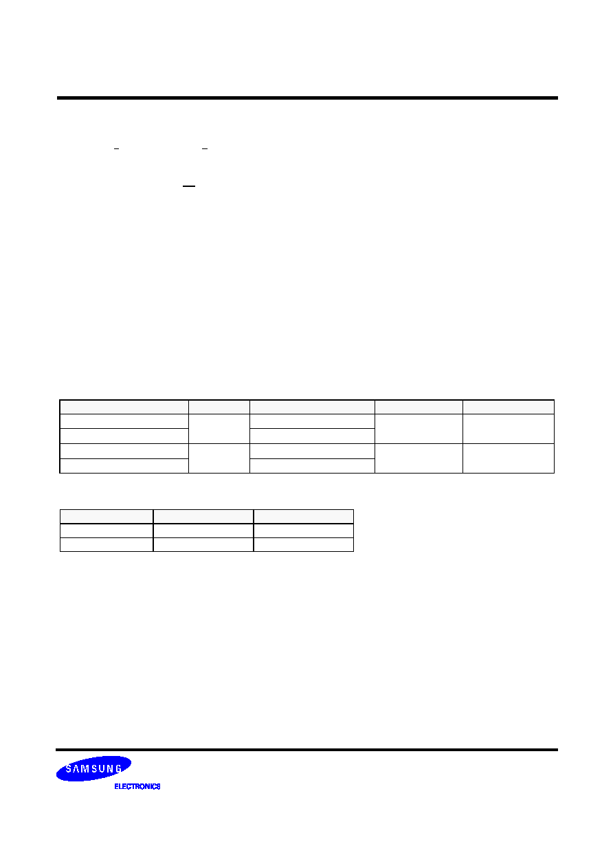
Ordering Information
Part No.
Org.
Max Freq.
Interface
Package
K4H560838D-TCCC
32M x 8
CC(DDR400@CL=3)
SSTL2
66pin TSOP II
K4H560838D-TCC4
C4(DDR400@CL=3)
K4H561638D-TCCC
16M x 16
CC(DDR400@CL=3)
SSTL2
66pin TSOP II
K4H561638D-TCC4
C4(DDR400@CL=3)
Key Features
*CL : CAS Latency
Operating Frequencies
- CC(DDR400@CL=3)
- C4(DDR400@CL=3)
Speed @CL3
200MHz
200MHz
CL-tRCD-tRP
3 - 3 - 3
3 - 4 - 4
DDR SDRAM
DDR SDRAM 256Mb D-die (x8, x16)
Rev. 1.1 Feb. 2003
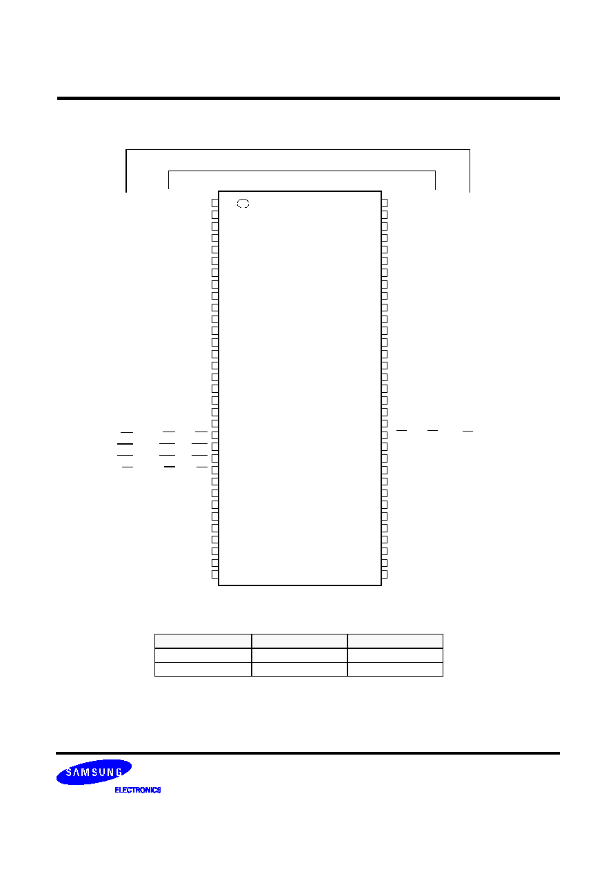
Pin Description
DM is internally loaded to match DQ and DQS identically.
256Mb Package Pinout
Row & Column address configuration
V
DD
1
66Pin TSOPII
(400mil x 875mil)
DQ
0
2
V
DDQ
3
NC
4
DQ
1
5
V
SSQ
6
NC
7
DQ
2
8
V
DDQ
9
NC
10
DQ
3
11
V
SSQ
12
BA
0
20
CS
19
RAS
18
CAS
17
WE
16
NC
15
V
DDQ
14
NC
13
V
DD
27
A
3
26
A
2
25
A
1
24
A
0
23
AP/A
10
22
BA
1
21
V
SS
54
DQ
7
53
V
SSQ
52
NC
51
DQ
6
50
V
DDQ
49
NC
48
DQ
5
47
V
SSQ
46
NC
45
DQ
4
44
V
DDQ
43
A
11
35
36
CKE
37
CK
38
DM
39
V
REF
40
V
SSQ
41
NC
42
V
SS
55
A
4
56
A
5
57
A
6
58
A
7
59
A
8
60
A
9
34
(0.65mm Pin Pitch)
33
32
31
30
29
28
61
62
63
64
65
66
NC
NC
NC
NC
NC
V
DD
NC
DQS
NC
V
SS
CK
NC
A
12
32Mb x 8
16Mb x 16
V
SS
NC
V
SSQ
NC
DQ
3
V
DDQ
NC
NC
V
SSQ
NC
DQ
2
V
DDQ
A
11
CKE
CK
DM
V
REF
V
SSQ
NC
V
SS
A
4
A
5
A
6
A
7
A
8
A
9
NC
DQS
NC
V
SS
CK
NC
A
12
V
SS
DQ
15
V
SSQ
DQ
14
DQ
13
V
DDQ
DQ
12
DQ
11
V
SSQ
DQ
10
DQ
9
V
DDQ
A
11
CKE
CK
UDM
V
REF
V
SSQ
DQ
8
V
SS
A
4
A
5
A
6
A
7
A
8
A
9
NC
UDQS
NC
V
SS
CK
NC
A
12
V
DD
NC
V
DDQ
NC
DQ
0
V
SSQ
NC
NC
V
DDQ
NC
DQ
1
V
SSQ
BA
0
CS
RAS
CAS
WE
NC
V
DDQ
NC
V
DD
A
3
A
2
A
1
A
0
AP/A
10
BA
1
NC
NC
NC
NC
NC
V
DD
V
DD
DQ
0
V
DDQ
DQ
1
DQ
2
V
SSQ
DQ
3
DQ
4
V
DDQ
DQ
5
DQ
6
V
SSQ
BA
0
CS
RAS
CAS
WE
LDM
V
DDQ
DQ
7
V
DD
A
3
A
2
A
1
A
0
AP/A
10
BA
1
NC
LDQS
NC
NC
NC
V
DD
Bank Address
BA0~BA1
Auto Precharge
A10
Organization
Row Address
Column Address
32Mx8
A0~A12
A0-A9
16Mx16
A0~A12
A0-A8
DDR SDRAM
DDR SDRAM 256Mb D-die (x8, x16)
Rev. 1.1 Feb. 2003
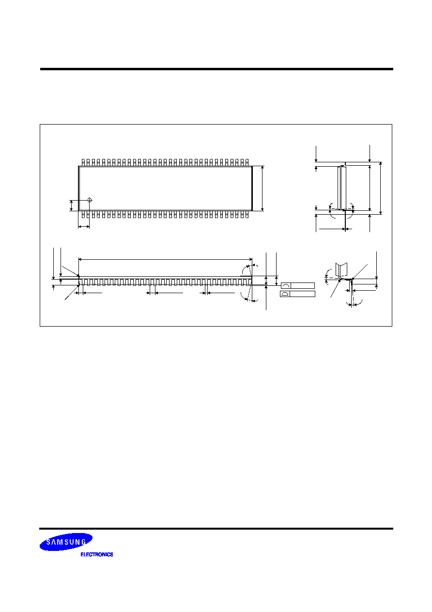
Units : Millimeters
0.30
±
0.08
0.65TYP
(0.71)
22.22
±
0.10
0.125
(0
.80
)
10
.1
6
±
0.
10
0
◊
~8
◊
#1
#33
#66
#34
(1.50)
(1
.5
0)
0.65
±
0.08
1.0
0
±
0.
10
1.
20
MAX
(0
.5
0)
(0
.5
0)
(1
0.
76
)
11
.
7
6
±
0.
2
0
(10
◊
)
(10
◊
)
+0.075
-0.035
(0
.8
0)
0.10 MAX
0.075 MAX
[
]
0.
05
MIN
(10
◊
)
(10
◊
)
(R0.1
5)
0.
21
0
±
0.
0
5
0.
66
5
±
0.
0
5
(R
0.
15
)
(4
◊
)
(R
0.
25
)
(R
0.
25
)
0.
45
~0
.7
5
0.25TYP
NOTE
1. ( ) IS REFERENCE
2. [ ] IS ASS
'
Y OUT QUALITY
66pin TSOPII / Package dimension
Package Physical Demension