- 1 -
Rev 1.0 (Mar 2005)
512M GDDR3 SDRAM
K4J52324QC-B
512Mbit GDDR3 SDRAM
Revision 1.0
March 2005
Samsung Electronics reserves the right to change products or specification without notice.
INFORMATION IN THIS DOCUMENT IS PROVIDED IN RELATION TO SAMSUNG PRODUCTS,
AND IS SUBJECT TO CHANGE WITHOUT NOTICE.
NOTHING IN THIS DOCUMENT SHALL BE CONSTRUED AS GRANTING ANY LICENSE,
EXPRESS OR IMPLIED, BY ESTOPPEL OR OTHERWISE,
TO ANY INTELLECTUAL PROPERTY RIGHTS IN SAMSUNG PRODUCTS OR TECHNOLOGY. ALL
INFORMATION IN THIS DOCUMENT IS PROVIDED
ON AS "AS IS" BASIS WITHOUT GUARANTEE OR WARRANTY OF ANY KIND.
1. For updates or additional information about Samsung products, contact your nearest Samsung office.
2. Samsung products are not intended for use in life support, critical care, medical, safety equipment, or similar
applications where Product failure could result in loss of life or personal or physical harm, or any military or
defense application, or any governmental procurement to which special terms or provisions may apply.

- 2 -
Rev 1.0 (Mar 2005)
512M GDDR3 SDRAM
K4J52324QC-B
Revision History
Revision 1.0 (March 8, 2005)
� Removed -BC10/11/12 from the spec.
� Separated VDD spec as below
- VDD & VDDQ = 2.0V + 0.1V distinguished by part number as -B
J
- VDD & VDDQ = 1.8V + 0.1V distinguished by part number as -B
C
Accordingly, defined -BJ12/14 and -BC14/16/20 along with supported operating voltage.
� Changed tRCDR and tRP of -BC16 from 9tCK and 8tCK to 10tCK and 9tCK. Accordingly, tRCDW/tRC/tDAL changed each from 5tCK/
27tCK/17tCK to 6tCK/28tCK/18tCK.
� Changed tRCDR and tRP of -BC20 from 7tCK and 6tCK to 8tCK and 7tCK. Accordingly, tRCDW/tRC/tDAL changed each from 4tCK/
21tCK/13tCK to 5tCK/22tCK/14tCK.
� Added Vendor ID read timing on page 18 & clock frequency change timing on page 19.
� Changed package dimension from 12mm x 14mm to 11mm x 14mm.
� DC spec updated.
� Capacitance values changed. Input(Clock,Address,Command) capacitance changed from 2.0pF/2.5pF to 1.5pF/3.0pF and DQ,DQS
and DM capacitance changed from 2.0pF/2.5pF to 1.5pF/2.0pF.

- 3 -
Rev 1.0 (Mar 2005)
512M GDDR3 SDRAM
K4J52324QC-B
Revision History
Revision 0.9 (November 11, 2004)
� Corrected typo in boundary scan order table.
Revision 0.8 (October 10, 2004)
� Changed part number from K4J52324QB-G to K4J52324Q
C-B
-Package code attribute re-defined : G .... 144FBGA, Leaded V .... 144FBGA, Lead-free
A .... 136FBGA, Leaded B .... 136FBGA, Lead-free
Revision 0.7 (October 5, 2004)
� DC spec defined.
� Comment added on how to change the clock frequency after the power-up (page 14)
� Comment added on read to write timing diagram on page 32 which specify the timing interval from data termination enable to the first
data-in should be greater than 1tCK.
� Changed CL(Cas Latency) of -GC14 from 9tCK to 10tCK . Changed CL(Cas Latency) of -GC16 from 8tCK to 9tCK
� Typo corrected in boundary scan order table and additional remark for boundary scan added on page 17.
� Changed tDCERR from 0.2tCK to 0.03tCK (Typo)
Revision 0.6 (September 15, 2004)
� Typo corrected
� Removed tWR_A to avoid confusion. Instead, tWR represent write recovery time for both normal precharge and Auto-precharge cases.
Accordingly tDAL adjusted by tWR for each frequency.
� Clock jitter spec added.
� Changed input capacitance.
�
Fixed CL of -GC12 to 11tCK where as specified with 10tCK or 11tCK previousely
.
Revision 0.5 (June 4, 2004)
� Typo corrected (Package ball out)
Revision 0.4 (May 13, 2004)
� Changed tRRD from 12ns to 10ns
� Added tFAW specification in the spec which defined as five times of tRRD
� Added boundary scan specification & added package dimension
Revision 0.3 (January 26, 2004)
� Changed part number of 512Mb(x32) GDDR3 from K4J53324QB-GC to K4J52324QB-GC
Revision 0.2 (January 5, 2004)
� Added Write Latency 5, 6, and 7 (clock) in the spec.
� Added tWR_A 8 and 9 (clock) in the spec.
Revision 0.1 (December 18, 2003)
� Changed CL of -GC12 from 9tCK to 10tCK
� Changed tCK(max) from 3.0ns to 3.3ns
Revision 0.0 (December 18 , 2003) -
Target Spec
- 4 -
Rev 1.0 (Mar 2005)
512M GDDR3 SDRAM
K4J52324QC-B
� 2.0V + 0.1V power supply for device operation for -BJ**
� 2.0V + 0.1V power supply for I/O interface for -BJ**
� 1.8V + 0.1V power supply for device operation for -BC**
� 1.8V + 0.1V power supply for I/O interface for -BC**
� On-Die Termination (ODT)
� Output Driver Strength adjustment by EMRS
� Calibrated output drive
� 1.8V Pseudo Open drain compatible inputs/outputs
� 4 internal banks for concurrent operation
� Differential clock inputs (CK and CK)
� Commands entered on each positive CK edge
� CAS latency : 4, 5, 6, 7, 8, 9, 10, 11 (clock)
� Additive latency (AL): 0 and 1 (clock)
� Programmable Burst length : 4 and 8
� Programmable Write latency : 1, 2, 3, 4, 5, 6 and 7 (clock)
GENERAL DESCRIPTION
FEATURES
� Single ended READ strobe (RDQS) per byte
� Single ended WRITE strobe (WDQS) per byte
� RDQS edge-aligned with data for READs
� WDQS center-aligned with data for WRITEs
� Data Mask(DM) for masking WRITE data
� Auto & Self refresh modes
� Auto Precharge option
� 32ms, auto refresh (8K cycle)
� 136 Ball FBGA
� Maximum clock frequency up to 800MHz
� Maximum data rate up to 1.6Gbps/pin
� DLL for outputs
� Boundary scan function with SEN pin
� Mirror function with MF pin
2M x 32Bit x 8 Banks Graphic Double Data Rate 3 Synchronous DRAM
with Uni-directional Data Strobe
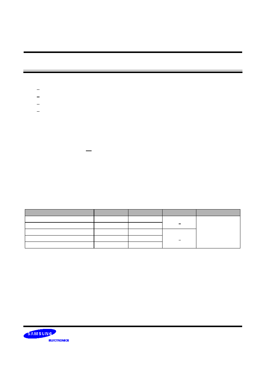
ORDERING INFORMATION
* K4J52324QC-A*** is leaded package part number
Part NO.
Max Freq.
Max Data Rate
VDD&VDDQ
Package
K4J52324QC-BJ12
800MHz
1.6Gbps/pin
2.0V+0.1V
136 Ball FBGA
K4J52324QC-BJ14
700MHz
1.4Gbps/pin
K4J52324QC-BC14
700MHz
1.4Gbps/pin
1.8V+0.1V
K4J52324QC-BC16
600MHz
1.2Gbps/pin
K4J52324QC-BC20
500MHz
1.0Gbps/pin
The K4J52324QC is 536,870,912 bits of hyper synchronous data rate Dynamic RAM organized as 8 x 2,097,152 words by
32 bits, fabricated with SAMSUNG
's
high performance CMOS technology. Synchronous features with Data Strobe allow
extremely high performance up to 6.4GB/s/chip. I/O transactions are possible on both edges of the clock cycle. Range of
operating frequencies, and programmable latencies allow the device to be useful for a variety of high performance memory
system applications.
FOR 2M x 32Bit x 8 Bank GDDR3 SDRAM
- 5 -
Rev 1.0 (Mar 2005)
512M GDDR3 SDRAM
K4J52324QC-B
PIN CONFIGURATION
Normal Package (Top View)
VDDQ
VDD
VSS
ZQ
VSSQ
DQ0
DQ1
VSSQ
VDDQ
DQ2
DQ3
VDDQ
VSSQ
WDQS0 RDQS0
VSSQ
VDDQ
DQ4
DM0
VDDQ
VDD
DQ6
DQ5
CAS
VSS
VSSQ
DQ7
BA0
VREF
A1
RAS
CKE
VSSA
RFU1
RFU2
VDDQ
VDDA
A10
A2
A0
VSS
VSSQ
DQ25
A11
VDD
DQ24
DQ27
A3
VDDQ
DQ26
DM3
VDDQ
VSSQ
WDQS3 RDQS3
VSSQ
VDDQ
DQ28
DQ29
VDDQ
VSSQ
DQ30
DQ31
VSSQ
VDDQ
VDD
VSS
SEN
MF
VSS
VDD
VDDQ
VSSQ
DQ9
DQ8
VSSQ
VDDQ
DQ11
DQ10
VDDQ
VSSQ
RDQS1 WDQS1
VSSQ
VDDQ
DM1
DQ12
VDDQ
CS
DQ13
DQ14
VDD
BA1
DQ15
VSSQ
VSS
WE
A5
VREF
VDDQ
CK
CK
VSSA
A4
A6
A8/AP
VDDA
A7
DQ17
VSSQ
VSS
A9
DQ19
DQ16
VDD
VDDQ
DM2
DQ18
VDDQ
VSSQ
RDQS2 WDQS2
VSSQ
VDDQ
DQ21
DQ20
VDDQ
VSSQ
DQ23
DQ22
VSSQ
RESET
VSS
VDD
VDDQ
1
2
3
4
5
6
7
8
9
10
11
12
A
B
C
D
E
F
G
H
J
K
L
M
N
P
R
T
V
BA2
NOTE :
1. RFU1 is reserved for future use
2. RFU2 is reserved for future use