
K4M28163PD-R(B)G/S
Rev. 1.3 Dec. 2002
CMOS SDRAM
Revision 1.3
December 2002
8Mx16
Mobile SDRAM
(VDD/VDDQ 1.8V/1.8V, TCSR & PASR & DS)
54CSP
K4M28163PD-R(B)G/S
Rev. 1.3 Dec. 2002
CMOS SDRAM
∑ 1.8V power supply.
∑ LVCMOS compatible with multiplexed address.
∑ Four banks operation.
∑ MRS cycle with address key programs.
-. CAS latency (1, 2 & 3).
-. Burst length (1, 2, 4, 8 & Full page).
-. Burst type (Sequential & Interleave).
∑ EMRS cycle with address key programs.
∑ All inputs are sampled at the positive going edge of the system
clock.
∑ Burst read single-bit write operation.
∑ Special Function Support.
-. PASR (Partial Array Self Refresh).
-. TCSR (Temperature Compensated Self Refresh)
-. DS (Driver Strength)
∑ DQM for masking.
∑ Auto refresh.
∑ 64ms refresh period (4K cycle).
∑ Extended Temperature Operation (-25
∞
C ~ 85
∞
C).
∑ 54balls CSP( -RXXX -Pb, -BXXX -Pb Free).
FEATURES
The K4M28163PD is 134,217,728 bits synchronous high data
rate Dynamic RAM organized as 4 x 2,097,152 words by 16
bits, fabricated with SAMSUNG
s high performance CMOS
technology. Synchronous design allows precise cycle control
with the use of system clock, and I/O transactions are possible
on every clock cycle. Range of operating frequencies, program-
mable burst lengths and programmable latencies allow the
same device to be useful for a variety of high bandwidth and
high performance memory system applications.
GENERAL DESCRIPTION
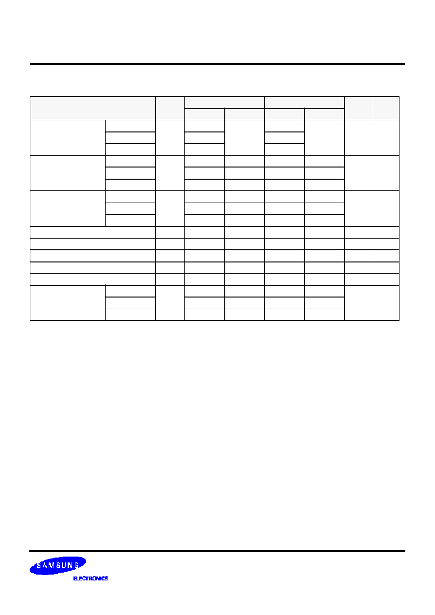
2M x 16Bit x 4 Banks Mobile SDRAM in 54CSP
Bank Select
Data Input Register
2M x 16
2M x 16
S
e
n
s
e
A
M
P
O
u
t
p
u
t
B
u
f
f
e
r
I
/
O
C
o
n
t
r
o
l
Column Decoder
Latency & Burst Length
Programming Register
A
d
d
r
e
s
s
R
e
g
i
s
t
e
r
R
o
w
B
u
f
f
e
r
R
e
f
r
e
s
h
C
o
u
n
t
e
r
R
o
w
D
e
c
o
d
e
r
C
o
l
.
B
u
f
f
e
r
L
R
A
S
L
C
B
R
LCKE
LRAS
LCBR
LWE
LDQM
CLK
CKE
CS
RAS
CAS
WE
LDQM
LWE
LDQM
DQi
CLK
ADD
LCAS
LWCBR
2M x 16
2M x 16
Timing Register
UDQM
* Samsung Electronics reserves the right to change products or specification without notice.
FUNCTIONAL BLOCK DIAGRAM
ORDERING INFORMATION
-R(B)G : Low Power, Operating Temp : -25
∞
C ~ 85
∞
C.
-R(B)S : Super Low Power, Operating Temp : -25
∞
C ~ 85
∞
C.
Notes :
1. In case of 40MHz Frequency, CL1 can be supported.
2. In case of 33MHz Frequency, CL1 can be supported.
Part No.
Max Freq.
Interface Package
K4M28163PD-R(B)G/S1L 105MHz(CL=3)
*1
LVCMOS
54 CSP
Pb
(Pb Free)
K4M28163PD-R(B)G/S15 66MHz(CL=2/3)
*2

K4M28163PD-R(B)G/S
Rev. 1.3 Dec. 2002
CMOS SDRAM
54Ball(6x9) CSP
1
2
3
7
8
9
A
V
SS
DQ15
V
SSQ
V
DDQ
DQ0
V
D D
B
DQ14
DQ13
V
DDQ
V
SSQ
DQ2
DQ1
C
DQ12
DQ11
V
SSQ
V
DDQ
DQ4
DQ3
D
DQ10
DQ9
V
DDQ
V
SSQ
DQ6
DQ5
E
DQ8
NC
V
SS
V
D D
LDQM
DQ7
F
UDQM
CLK
CKE
CAS
RAS
WE
G
NC
A11
A9
BA0
BA1
CS
H
A8
A7
A6
A0
A1
A10
J
V
SS
A5
A4
A3
A2
V
D D
Pin Name
Pin Function
CLK
System Clock
CS
Chip Select
CKE
Clock Enable
A
0
~ A
11
Address
BA
0
~ BA
1
Bank Select Address
RAS
Row Address Strobe
CAS
Column Address Strobe
WE
Write Enable
L(U)DQM
Data Input/Output Mask
DQ
0
~
15
Data Input/Output
V
DD
/V
SS
Power Supply/Ground
V
DDQ
/V
SSQ
Data Output Power/Ground
Package Dimension and Pin Configuration
< Bottom View
*1
>
< Top View
*2
>
< Top View
*2
>
*2: Top View
Symbol
Min
Typ
Max
A
0.90
0.95
1.00
A
1
0.30
0.35
0.40
E
-
8.10
-
E
1
-
6.40
-
D
-
9.30
-
D
1
-
6.40
-
e
-
0.80
-
b
0.40
0.45
0.50
z
-
-
0.10
[Unit:mm]
5
2
1
6
3
4
8
9
7
F
E
D
C
B
J
H
G
A
e
D
D
/
2
D
1
E
1
E
E/2
A
A1
z
b
Encapsulant
Max. 0.20
*1: Bottom View
#A1 Ball Origin Indicator
K
4
M
2
8
1
6
3
P
D
-
X
X
X
X
S
A
M
S
U
N
G
W
e
e
k
K4M28163PD-R(B)G/S
Rev. 1.3 Dec. 2002
CMOS SDRAM
DC OPERATING CONDITIONS
Recommended operating conditions (Voltage referenced to V
SS
= 0V, T
A
= -25
∞
C to 85
∞
C)
Notes :
1. V
IH
(max) = 2.2V AC.The overshoot voltage duration is
3ns.
2. V
IL
(min) = -1.0V AC. The undershoot voltage duration is
3ns.
3. Any input 0V
V
IN
V
DDQ
.
Input leakage currents include Hi-Z output leakage for all bi-directional buffers with tri-state outputs.
4. Dout is disabled, 0V
V
OUT
V
DDQ.
Parameter
Symbol
Min
Typ
Max
Unit
Note
Supply voltage
V
D D
1.65
1.8
1.95
V
V
DDQ
1.65
1.8
1.95
V
Input logic high voltage
V
I H
0.8 x V
DDQ
1.8
V
DDQ
+ 0.3
V
1
Input logic low voltage
V
IL
-0.3
0
0.3
V
2
Output logic high voltage
V
O H
V
DDQ
- 0.2
-
-
V
I
O H
= -0.1mA
Output logic low voltage
V
OL
-
-
0.2
V
I
OL
= 0.1mA
Input leakage current
I
LI
-10
-
10
uA
3
CAPACITANCE
(V
DD
= 1.8V, T
A
= 23
∞
C, f = 1MHz, V
REF
=0.9V
±
50
mV)
Pin
Symbol
Min
Max
Unit
Note
Clock
C
CLK
2.0
4.0
pF
RAS, CAS, WE, CS, CKE, DQM
C
IN
2.0
4.0
pF
Address
C
ADD
2.0
4.0
pF
DQ
0
~ DQ
15
C
OUT
3.5
6.0
pF
ABSOLUTE MAXIMUM RATINGS
Notes :
Permanent device damage may occur if ABSOLUTE MAXIMUM RATINGS are exceeded.
Functional operation should be restricted to recommended operating condition.
Exposure to higher than recommended voltage for extended periods of time could affect device reliability.
Parameter
Symbol
Value
Unit
Voltage on any pin relative to Vss
V
I N
, V
OUT
-1.0 ~ 2.6
V
Voltage on V
D D
supply relative to Vss
V
DD
, V
DDQ
-1.0 ~ 2.6
V
Storage temperature
T
STG
-55 ~ +150
∞
C
Power dissipation
P
D
1
W
Short circuit current
I
OS
50
mA
K4M28163PD-R(B)G/S
Rev. 1.3 Dec. 2002
CMOS SDRAM
DC CHARACTERISTICS
Recommended operating conditions (Voltage referenced to V
SS
= 0V, T
A
= -25 to 85
∞
C)
Notes :
1. Measured with outputs open.
2. Refresh period is 64ms.
3. K4M28163PD-R(B)G**
4. K4M28163PD-R(B)S**
5. Unless otherwise noted, input swing IeveI is CMOS(V
IH
/V
IL
=V
DDQ
/V
SSQ
).
Parameter
Symbol
Test Condition
Version
Unit
Note
-1L
-15
Operating Current
(One Bank Active)
I
CC1
Burst length = 1
t
RC
t
R C
(min)
I
O
= 0 mA
35
30
mA
1
Precharge Standby Current
in power-down mode
I
CC2
P
CKE
V
IL
(max), t
CC
= 10ns
0.3
mA
I
C C 2
PS CKE & CLK
V
IL
(max), t
CC
=
0.3
Precharge Standby Current
in non power-down mode
I
CC2
N
CKE
V
IH
(min), CS
V
IH
(min), t
CC
= 10ns
Input signals are changed one time during
20ns
5.5
mA
I
CC2
NS
CKE
V
IH
(min), CLK
V
IL
(max), t
CC
=
Input signals are stable
1
Active Standby Current
in power-down mode
I
CC3
P
CKE
V
IL
(max), t
CC
= 10ns
1.5
mA
I
C C 3
PS CKE & CLK
V
IL
(max), t
CC
=
1
Active Standby Current
in non power-down mode
(One Bank Active)
I
CC3
N
CKE
V
IH
(min), CS
V
IH
(min), t
CC
= 10ns
Input signals are changed one time during
20ns
12
mA
I
CC3
NS
CKE
V
IH
(min), CLK
V
IL
(max), t
CC
=
Input signals are stable
6
mA
Operating Current
(Burst Mode)
I
CC4
I
O
= 0 mA
Page burst
4Banks Activated
t
CCD
= 2CLKs
50
40
mA
1
Refresh Current
I
CC5
t
RC
t
R C
(min)
85
75
mA
2
Self Refresh Current
I
CC6
CKE
0.2V
TCSR Range
Max 45
∞
C
Max 85
∞
C
∞
C
-R(B)G
4 Banks
160
200
uA
3
2 Banks
140
160
1 Bank
130
140
-R(B)S
4 Banks
100
140
4
2 Banks
80
100
1 Bank
70
80
K4M28163PD-R(B)G/S
Rev. 1.3 Dec. 2002
CMOS SDRAM
1.8V
13.9K
10.6K
Output
30pF
V
OH
(DC) = V
DDQ
-0.2 , I
O H
= -0.1mA
V
OL
(DC) = 0.2V, I
OL
= 0.1mA
Vtt=0.5 x V
DDQ
50
Output
30pF
Z0=50
(Fig. 2) AC Output Load Circuit
(Fig. 1) DC Output Load Circuit
OPERATING AC PARAMETER
AC OPERATING TEST CONDITIONS
(V
DD
= 1.8V
±
0.15V, T
A
= -25
∞
C to 85
∞
C)
Parameter
Value
Unit
AC input levels (Vih/Vil)
0.9 x V
DDQ
/ 0.2
V
Input timing measurement reference level
0.5 x V
DDQ
V
Input rise and fall time
tr/tf = 1/1
ns
Output timing measurement reference level
0.5 x V
DDQ
V
Output load condition
See Fig. 2
(AC operating conditions unless otherwise noted .)
Notes :
1. The minimum number of clock cycles is determined by dividing the minimum time required with clock cycle time
and then rounding off to the next higher integer.
2. Minimum delay is required to complete write.
3. Minimum tRDL=2CLK and tDAL(=tRDL + tRP) is required to complete both of last data wite command(tRDL) and precharge
command(tRP). tRDL=1CLK can be supported only in the case under 100MHz with manual precharge mode.
4. All parts allow every cycle column address change.
5. In case of row precharge interrupt, auto precharge and read burst stop.
Parameter
Symbol
Version
Unit
Note
-1L
-15
Row active to row active delay
t
RRD
(min)
19
30
ns
1
RAS to CAS delay
t
RCD
(min)
28.5
30
ns
1
Row precharge time
t
R P
(min)
28.5
30
ns
1
Row active time
t
RAS
(min)
60
60
ns
1
t
RAS
(max)
100
us
Row cycle time
t
R C
(min)
90
90
ns
1
Last data in to row precharge
t
R D L
(min)
2
CLK
2,3
Last data in to Active delay
t
DAL
(min)
tRDL + tRP
-
3
Last data in to new col. address delay
t
C D L
(min)
1
CLK
2
Last data in to burst stop
t
BDL
(min)
1
CLK
2
Auto refresh cycle time
t
ARFC
(min)
105
ns
Exit self refresh to write command
t
SRFX
(min)
120
ns
Col. address to col. address delay
t
CCD
(min)
1
CLK
4
Number of valid output data
CAS latency=3
2
ea
5
CAS latency=2
1
CAS latency=1
0
K4M28163PD-R(B)G/S
Rev. 1.3 Dec. 2002
CMOS SDRAM
(AC operating conditions unless otherwise noted.)
Notes :
1. Parameters depend on programmed CAS latency.
2. If clock rising time is longer than 1ns, (tr/2-0.5)ns should be added to the parameter.
3. Assumed input rise and fall time (tr & tf) = 1ns.
If tr & tf is longer than 1ns, transient time compensation should be considered,
i.e., [(tr + tf)/2-1]ns should be added to the parameter.
Parameter
Symbol
-1L
- 15
Unit
Note
Min
Max
Min
Max
CLK cycle time
CAS latency=3
t
C C
9.5
1000
15
1000
ns
1
CAS latency=2
15
15
CAS latency=1
25
30
CLK to valid output delay
CAS latency=3
t
SAC
7
9
ns
1,2
CAS latency=2
8
9
CAS latency=1
20
24
Output data hold time
CAS latency=3
t
O H
2.5
2.5
ns
2
CAS latency=2
2.5
2.5
CAS latency=1
2.5
2.5
CLK high pulse width
t
C H
3.5
3.5
ns
3
CLK low pulse width
t
C L
3.5
3.5
ns
3
Input setup time
t
SS
3.0
4.0
ns
3
Input hold time
t
SH
1.5
2.0
ns
3
CLK to output in Low-Z
t
SLZ
1
1
ns
2
CLK to output in Hi-Z
CAS latency=3
t
SHZ
7
9
ns
CAS latency=2
8
9
CAS latency=1
20
24
AC CHARACTERISTICS
Note :
1. Samsung are not designed or manufactured for use in a device or system that is used under circumstance in which human life is
potentially at stake. Please contact to the memory marketing team in samsung electronics when considering the use of a product con-
tained herein for any specific purpose, such as medical, aerospace, nuclear, military, vehicular or undersea repeater use.
K4M28163PD-R(B)G/S
Rev. 1.3 Dec. 2002
CMOS SDRAM
SIMPLIFIED TRUTH TABLE
(V=Valid, X=Don
t Care, H=Logic High, L=Logic Low)
Notes :
1. OP Code : Operand Code
A
0
~ A
11
& BA
0
~ BA
1
: Program keys. (@MRS)
2. MRS can be issued only at all banks precharge state.
A new command can be issued after 2 CLK cycles of MRS.
3. Auto refresh functions are the same as CBR refresh of DRAM.
The automatical precharge without row precharge command is meant by "Auto".
Auto/self refresh can be issued only at all banks precharge state.
Partial self refresh can be issued only after setting partial self refresh mode.
4. BA
0
~ BA
1
: Bank select addresses.
If both BA
0
and BA
1
are "Low" at read, write, row active and precharge, bank A is selected.
If BA
0
is "Low" and BA
1
is "High" at read, write, row active and precharge, bank B is selected.
If BA
0
is "High" and BA
1
is "Low" at read, write, row active and precharge, bank C is selected.
If both BA
0
and BA
1
are "High" at read, write, row active and precharge, bank D is selected.
If A
10
/AP is "High" at row precharge, BA
0
and BA
1
is ignored and all banks are selected.
5. During burst read or write with auto precharge, new read/write command can not be issued.
Another bank read/write command can be issued after the end of burst.
New row active of the associated bank can be issued at t
RP
after the end of burst.
6. Burst stop command is valid at every burst length.
7. DQM sampled at the positive going edge of CLK masks the data-in at that same CLK in write operation (Write DQM latency
is 0), but in read operation makes the data-out Hi-Z state after 2 CLK cycles. (Read DQM latency is 2).
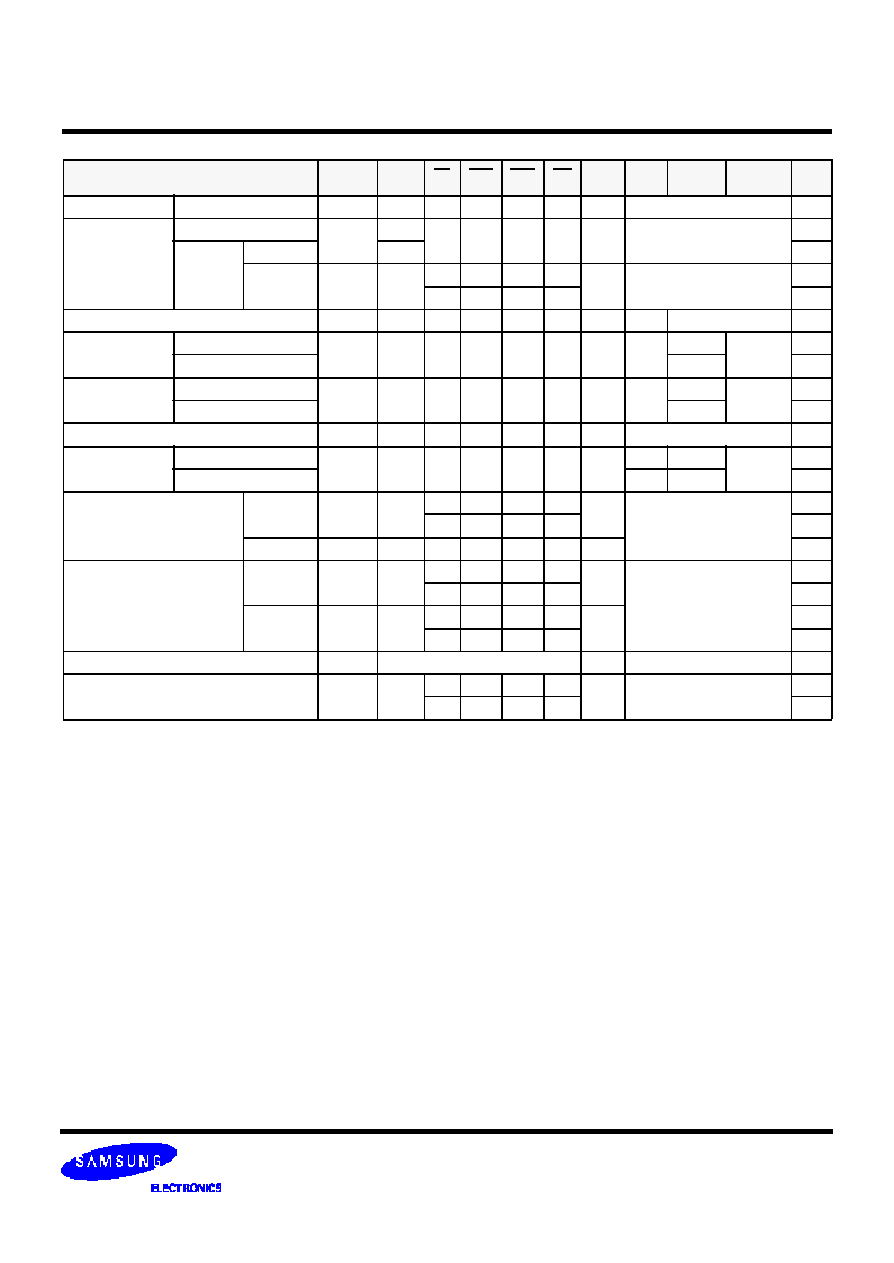
COMMAND
CKEn-1
CKEn
CS
RAS
CAS
WE
DQM
BA
0,1
A
10
/AP
A
11,
A
9
~ A
0
Note
Register
Mode Register Set
H
X
L
L
L
L
X
OP CODE
1, 2
Refresh
Auto Refresh
H
H
L
L
L
H
X
X
3
Self
Refresh
Entry
L
3
Exit
L
H
L
H
H
H
X
X
3
H
X
X
X
3
Bank Active & Row Addr.
H
X
L
L
H
H
X
V
Row Address
Read &
Column Address
Auto Precharge Disable
H
X
L
H
L
H
X
V
L
Column
Address
(A
0
~ A
8
)
4
Auto Precharge Enable
H
4, 5
Write &
Column Address
Auto Precharge Disable
H
X
L
H
L
L
X
V
L
Column
Address
(A
0
~ A
8
)
4
Auto Precharge Enable
H
4, 5
Burst Stop
H
X
L
H
H
L
X
X
6
Precharge
Bank Selection
H
X
L
L
H
L
X
V
L
X
All Banks
X
H
Clock Suspend or
Active Power Down
Entry
H
L
H
X
X
X
X
X
L
V
V
V
Exit
L
H
X
X
X
X
X
Precharge Power Down Mode
Entry
H
L
H
X
X
X
X
X
L
H
H
H
Exit
L
H
H
X
X
X
X
L
V
V
V
DQM
H
X
V
X
7
No Operation Command
H
X
H
X
X
X
X
X
L
H
H
H