K4M56163PE - R(B)G/F
February 2004
Mobile-SDRAM
· 1.8V power supply.
· LVCMOS compatible with multiplexed address.
· Four banks operation.
· MRS cycle with address key programs.
-. CAS latency (1, 2 & 3).
-. Burst length (1, 2, 4, 8 & Full page).
-. Burst type (Sequential & Interleave).
· EMRS cycle with address key programs.
· All inputs are sampled at the positive going edge of the system
clock.
· Burst read single-bit write operation.
· Special Function Support.
-. PASR (Partial Array Self Refresh).
-. Internal TCSR (Temperature Compensated Self Refresh)
-. DS (Driver Strength)
· DQM for masking.
· Auto refresh.
· 64ms refresh period (8K cycle).
· Commercial Temperature Operation (-25
°
C ~ 70
°
C).
· Extended Temperature Operation (-25
°
C ~ 85
°
C).
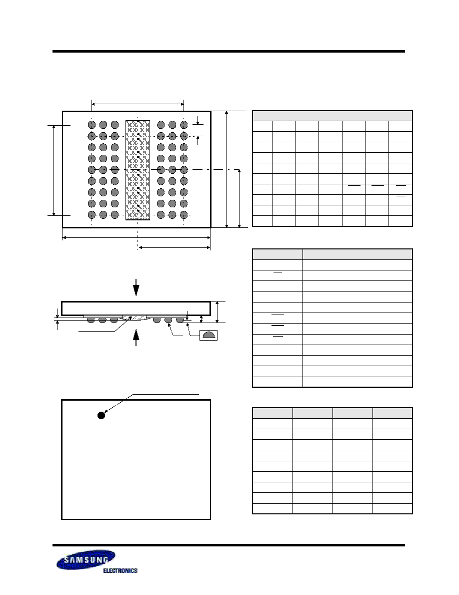
· 54Balls FBGA with 0.8mm ball pitch
( -RXXX : Leaded, -BXXX : Lead Free).
FEATURES
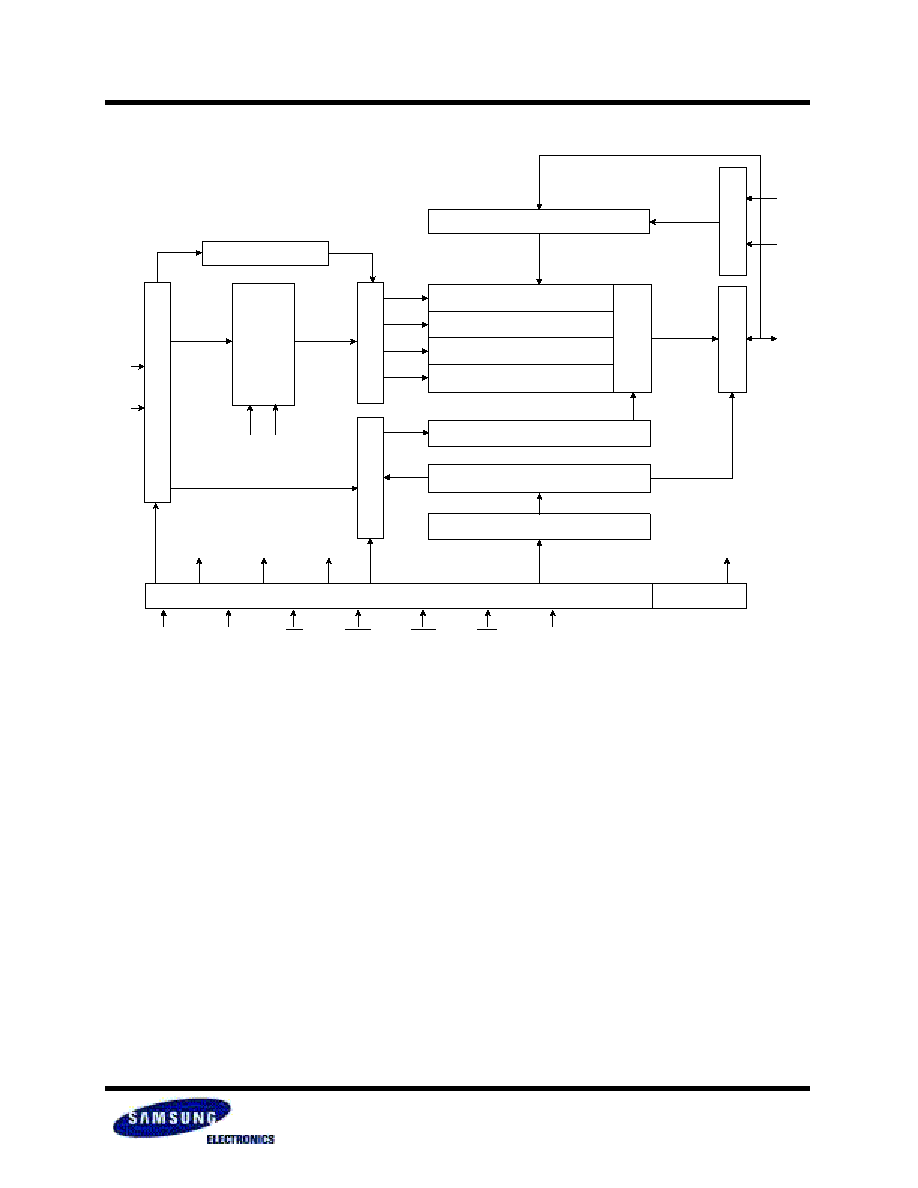
The K4M56163PE is 268,435,456 bits synchronous high data
rate Dynamic RAM organized as 4 x 4,196,304 words by 16 bits,
fabricated with SAMSUNG's high performance CMOS technol-
ogy. Synchronous design make a device controlled precisely
with the use of system clock and I/O transactions are possible
on every clock cycle. The range of operating frequencies, pro-
grammable burst lengths and programmable latencies allow the
same device to be useful for a variety of high bandwidth and
high performance memory system applications.
GENERAL DESCRIPTION
ORDERING INFORMATION
- R(B)G : Low Power, Extended Temperature(-25
°
C ~ 85
°
C)
- R(B)F : Low Power, Commercial Temperature(-25
°
C ~ 70
°
C)
Notes :
1. In case of 40MHz Frequency, CL1 can be supported.
2. Samsung are not designed or manufactured for use in a device or system that is used under circumstance in which human life is potentially at stake.
Please contact to the memory marketing team in samsung electronics when considering the use of a product contained herein for any specific
purpose, such as medical, aerospace, nuclear, military, vehicular or undersea repeater use.
Part No.
Max Freq.
Interface
Package
K4M56163PE-R(B)G/F90
111MHz(CL=3), 83MHz(CL=2)
LVCMOS
54 FBGA
Leaded (Lead Free)
K4M56163PE-R(B)G/F1L
105MHz(CL=3), 66MHz(CL=2)
*1
4M x 16Bit x 4 Banks Mobile SDRAM in 54FBGA
K4M56163PE - R(B)G/F
February 2004
Mobile-SDRAM
DC OPERATING CONDITIONS
Recommended operating conditions (Voltage referenced to V
SS
= 0V, T
A
= -25 to 85
°
C for Extended, -25 to 70
°
C for Commercial )
NOTES :
1. VIH (max) = 2.2V AC.The overshoot voltage duration is
3ns.
2. VIL (min) = -1.0V AC. The undershoot voltage duration is
3ns.
3. Any input 0V
VIN
VDDQ.
Input leakage currents include Hi-Z output leakage for all bi-directional buffers with tri-state outputs.
4. Dout is disabled, 0V
VOUT
VDDQ.
Parameter
Symbol
Min
Typ
Max
Unit
Note
Supply voltage
V
DD
1.7
1.8
1.95
V
V
DDQ
1.7
1.8
1.95
V
Input logic high voltage
V
IH
0.8 x V
DDQ
1.8
V
DDQ
+ 0.3
V
1
Input logic low voltage
V
IL
-0.3
0
0.3
V
2
Output logic high voltage
V
OH
V
DDQ
-0.2
-
-
V
I
OH
= -0.1mA
Output logic low voltage
V
OL
-
-
0.2
V
I
OL
= 0.1mA
Input leakage current
I
LI
-10
-
10
uA
3
CAPACITANCE
(V
DD
= 1.8V, T
A
= 23
°
C, f = 1MHz, V
REF
=0.9V
±
50 mV)
Pin
Symbol
Min
Max
Unit
Note
Clock
C
CLK
2.0
4.0
pF
RAS, CAS, WE, CKE, DQM
C
IN
2.0
4.0
pF
CS
C
IN
2.0
4.0
pF
Address
C
ADD
2.0
4.0
pF
DQ
0
~ DQ
15
C
OUT
3.0
5.0
pF
ABSOLUTE MAXIMUM RATINGS
NOTES:
Permanent device damage may occur if ABSOLUTE MAXIMUM RATINGS are exceeded.
Functional operation should be restricted to recommended operating condition.
Exposure to higher than recommended voltage for extended periods of time could affect device reliability.
Parameter
Symbol
Value
Unit
Voltage on any pin relative to V
ss
V
IN
, V
OUT
-1.0 ~ 2.6
V
Voltage on V
DD
supply relative to V
ss
V
DD
, V
DDQ
-1.0 ~ 2.6
V
Storage temperature
T
STG
-55 ~ +150
°
C
Power dissipation
P
D
1.0
W
Short circuit current
I
OS
50
mA
K4M56163PE - R(B)G/F
February 2004
Mobile-SDRAM
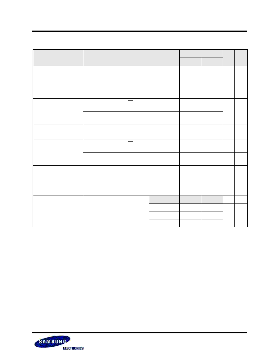
DC CHARACTERISTICS
Recommended operating conditions (Voltage referenced to V
SS
= 0V, T
A
= -25 to 85
°
C for Extended, -25 to 70
°
C for Commercial)
NOTES:
1. Measured with outputs open.
2. Refresh period is 64ms.
3. Unless otherwise noted, input swing IeveI is CMOS(VIH /VIL=VDDQ/VSSQ).
Parameter
Symbol
Test Condition
Version
Unit
Note
-90
-1L
Operating Current
(One Bank Active)
I
CC1
Burst length = 1
t
RC
t
RC
(min)
I
O
= 0 mA
45
40
mA
1
Precharge Standby Current in
power-down mode
I
CC2
P
CKE
V
IL
(max), t
CC
= 10ns
0.3
mA
I
CC2
PS CKE & CLK
V
IL
(max), t
CC
=
0.3
Precharge Standby Current
in non power-down mode
I
CC2
N
CKE
V
IH
(min), CS
V
IH
(min), t
CC
= 10ns
Input signals are changed one time during 20ns
10
mA
I
CC2
NS
CKE
V
IH
(min), CLK
V
IL
(max), t
CC
=
Input signals are stable
1
Active Standby Current
in power-down mode
I
CC3
P
CKE
V
IL
(max), t
CC
= 10ns
5
mA
I
CC3
PS CKE & CLK
V
IL
(max), t
CC
=
1
Active Standby Current
in non power-down mode
(One Bank Active)
I
CC3
N
CKE
V
IH
(min), CS
V
IH
(min), t
CC
= 10ns
Input signals are changed one time during 20ns
20
mA
I
CC3
NS
CKE
V
IH
(min), CLK
V
IL
(max), t
CC
=
Input signals are stable
5
mA
Operating Current
(Burst Mode)
I
CC
4
I
O
= 0 mA
Page burst
4Banks Activated
t
CCD
= 2CLKs
65
60
mA
1
Refresh Current
I
CC
5
t
ARFC
t
ARFC
(min)
80
80
mA
2
Self Refresh Current
I
CC
6
CKE
0.2V
TCSR Range
Max 40
Max 85/70
°
C
Full Array
150
400
uA
1/2 of Full Array
125
300
1/4 of Full Array
115
250