K4M56323PG-F(H)E/G/C/F
January 2006
Mobile-SDRAM
∑ 1.8V power supply.
∑ LVCMOS compatible with multiplexed address.
∑ Four banks operation.
∑ MRS cycle with address key programs.
-. CAS latency (1, 2 & 3).
-. Burst length (1, 2, 4, 8 & Full page).
-. Burst type (Sequential & Interleave).
∑ EMRS cycle with address key programs.
∑ All inputs are sampled at the positive going edge of the system
clock.
∑ Burst read single-bit write operation.
∑ Special Function Support.
-. PASR (Partial Array Self Refresh).
-. Internal TCSR (Temperature Compensated Self Refresh)
-. DS (Driver Strength)
-. DPD (Deep Power Down)
∑ DQM for masking.
∑ Auto refresh.
∑ 64ms refresh period (4K cycle).
∑ Commercial Temperature Operation (-25
∞
C ~ 70
∞
C).
∑ Extended Temperature Operation (-25
∞
C ~ 85
∞
C).
∑ 90Balls FBGA ( -FXXX -Pb, -HXXX -Pb Free).
FEATURES
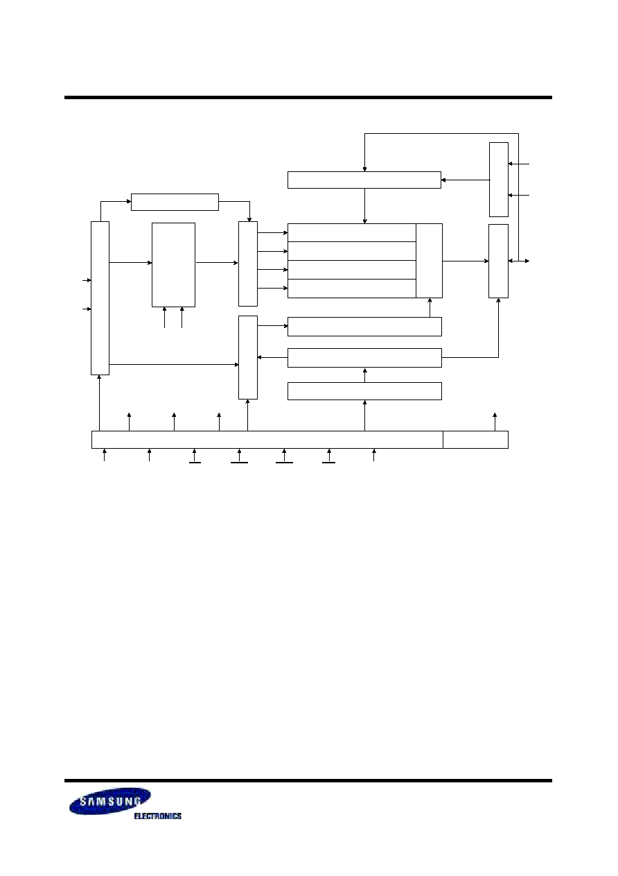
The K4M56323PG is 268,435,456 bits synchronous high data
rate Dynamic RAM organized as 4 x 2,097,152 words by 32 bits,
fabricated with SAMSUNG's high performance CMOS technol-
ogy. Synchronous design allows precise cycle control with the
use of system clock and I/O transactions are possible on every
clock cycle. Range of operating frequencies, programmable
burst lengths and programmable latencies allow the same
device to be useful for a variety of high bandwidth and high per-
formance memory system applications.
GENERAL DESCRIPTION
ORDERING INFORMATION
- F(H)E/G : Normal/ Low Power, Extended Temperature(-25
∞
C ~ 85
∞
C)
- F(H)C/F : Normal/ Low Power, Commercial Temperature(-25
∞
C ~ 70
∞
C)
NOTES :
1. In case of 40MHz Frequency, CL1 can be supported.
Part No.
Max Freq.
Interface
Package
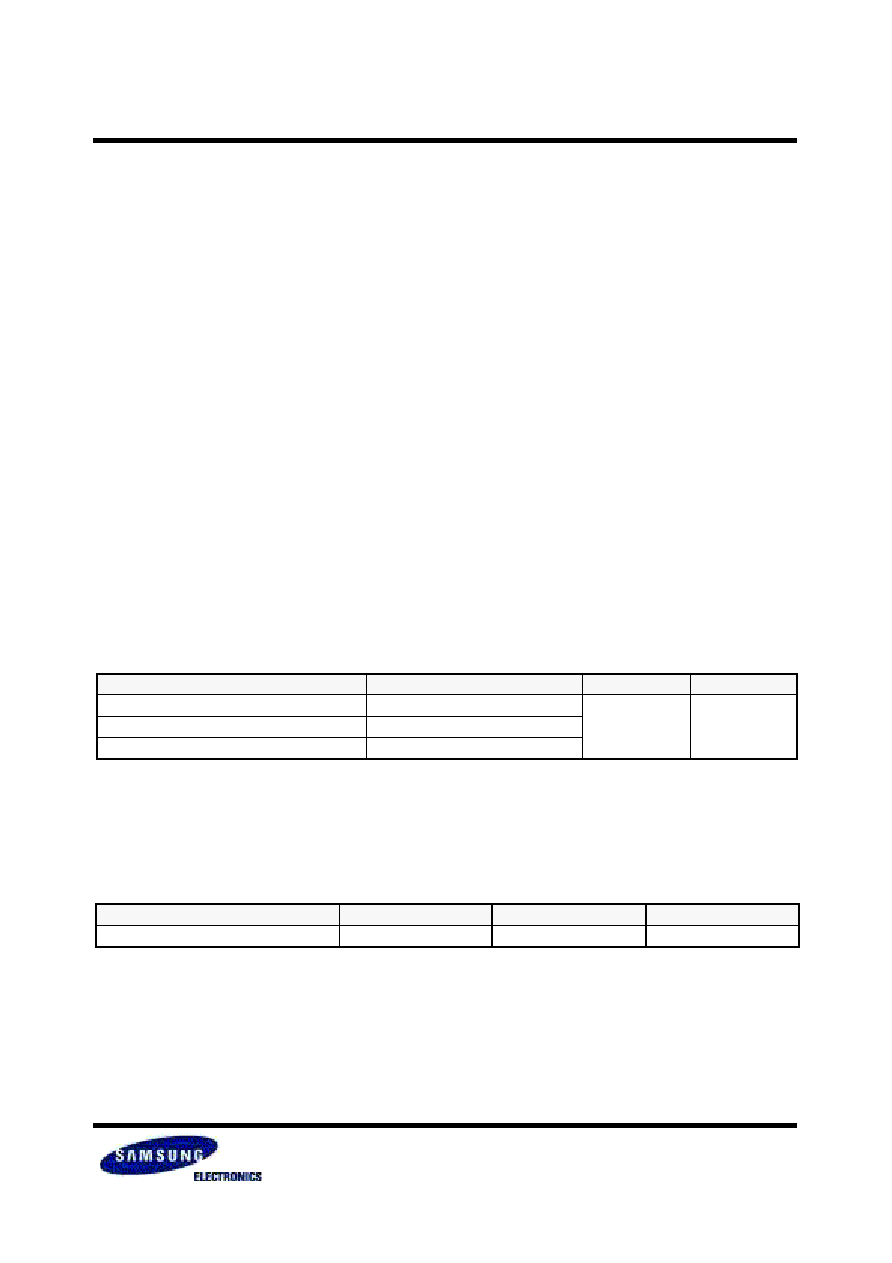
K4M56323PG-F(H)E/G/C/F75
133MHz(CL=3), 83MHz(CL2)
LVCMOS
90 FBGA Pb
(Pb Free)
K4M56323PG-F(H)E/G/C/F90
111MHz(CL=3), 83MHz(CL2)
K4M56323PG-F(H)E/G/C/F1L
111MHz(CL=3)
*1
, 66MHz(CL2)
2M x 32Bit x 4 Banks Mobile SDRAM in 90FBGA
Address configuration
Organization
Bank
Row
Column Address
8Mx32
BA0,BA1
A0 - A11
A0 - A8
INFORMATION IN THIS DOCUMENT IS PROVIDED IN RELATION TO SAMSUNG PRODUCTS, AND IS SUBJECT TO CHANGE WITHOUT NOTICE.
NOTHING IN THIS DOCUMENT SHALL BE CONSTRUED AS GRANTING ANY LICENSE, EXPRESS OR IMPLIED, BY ESTOPPEL OR OTHERWISE,
TO ANY INTELLECTUAL PROPERTY RIGHTS IN SAMSUNG PRODUCTS OR TECHNOLOGY. ALL INFORMATION IN THIS DOCUMENT IS PRO-
VIDED ON AS "AS IS" BASIS WITHOUT GUARANTEE OR WARRANTY OF ANY KIND.
1. For updates or additional information about Samsung products, contact your nearest Samsung office.
2. Samsung products are not intended for use in life support, critical care, medical, safety equipment, or similar applications where Product failure could
result in loss of life or personal or physical harm, or any military or defense application, or any governmental procurement to which special terms or pro-
visions may apply.
K4M56323PG-F(H)E/G/C/F
January 2006
Mobile-SDRAM
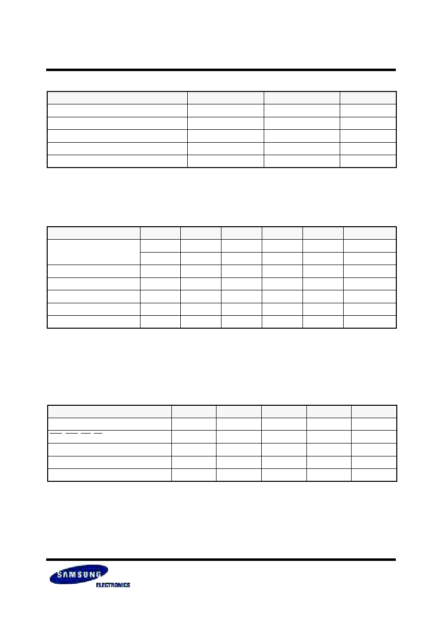
DC OPERATING CONDITIONS
Recommended operating conditions (Voltage referenced to V
SS
= 0V, T
A
= -25 to 85
∞
C for Extended, -25 to 70
∞
C for Commercial)
NOTES :
1. Under all conditions VDDQ must be less than or equal to VDD.
2. VIH (max) = 2.2V AC.The overshoot voltage duration is
3ns.
3. VIL (min) = -1.0V AC. The undershoot voltage duration is
3ns.
4. Any input 0V
VIN
VDDQ.
Input leakage currents include Hi-Z output leakage for all bi-directional buffers with tri-state outputs.
5. Dout is disabled, 0V
VOUT
VDDQ.
Parameter
Symbol
Min
Typ
Max
Unit
Note
Supply voltage
V
DD
1.7
1.8
1.95
V
1
V
DDQ
1.7
1.8
1.95
V
1
Input logic high voltage
V
IH
0.8 x V
DDQ
-
V
DDQ
+ 0.3
V
2
Input logic low voltage
V
IL
-0.3
0
0.3
V
3
Output logic high voltage
V
OH
V
DDQ
-0.2
-
-
V
I
OH
= -0.1mA
Output logic low voltage
V
OL
-
-
0.2
V
I
OL
= 0.1mA
Input leakage current
I
LI
-2
-
2
uA
4
CAPACITANCE
(V
DD
= 1.8V, T
A
= 23
∞
C, f = 1MHz, V
REF
=0.9V
±
50 mV)
Pin
Symbol
Min
Max
Unit
Note
Clock
C
CLK
1.5
3.5
pF
RAS, CAS, WE, CS, CKE
C
IN
1.5
3.0
pF
DQM
C
IN
1.5
3.0
pF
Address
C
ADD
1.5
3.0
pF
DQ
0
~ DQ
31
C
OUT
2.0
4.5
pF
ABSOLUTE MAXIMUM RATINGS
NOTES:
Permanent device damage may occur if ABSOLUTE MAXIMUM RATINGS are exceeded.
Functional operation should be restricted to recommended operating condition.
Exposure to higher than recommended voltage for extended periods of time could affect device reliability.
Parameter
Symbol
Value
Unit
Voltage on any pin relative to V
ss
V
IN
, V
OUT
-1.0 ~ 2.6
V
Voltage on V
DD
supply relative to V
ss
V
DD
, V
DDQ
-1.0 ~ 2.6
V
Storage temperature
T
STG
-55 ~ +150
∞
C
Power dissipation
P
D
1.0
W
Short circuit current
I
OS
50
mA
K4M56323PG-F(H)E/G/C/F
January 2006
Mobile-SDRAM
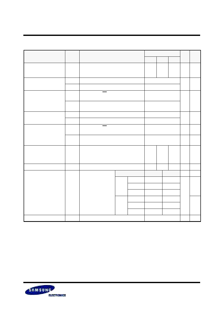
DC CHARACTERISTICS
Recommended operating conditions (Voltage referenced to V
SS
= 0V, T
A
= -25 to 85
∞
C for Extended, -25 to 70
∞
C for Commercial)
NOTES:
1. Measured with outputs open.
2. Refresh period is 64ms.
3. Internal TCSR can be supported.
In comercial Temp : 45
∞
C/Max 70
∞
C. In extended Temp : 45
∞
C/Max 85
∞
C.
4. It has +/-5
∞
C tolerance.
5. K4M56323PG-F(H)E/C
**
6. K4M56323PG-F(H)G/F
**
7. DPD(Deep Power Down) function is an optional feature, and it will be enabled upon request.
Please contact Samsung for more information.
8. Unless otherwise noted, input swing IeveI is CMOS(VIH /VIL=VDDQ/VSSQ).
Parameter
Symbol
Test Condition
Version
Unit
Note
-75
-90
-1L
Operating Current
(One Bank Active)
I
CC1
Burst length = 1
t
RC
t
RC
(min)
I
O
= 0 mA
65
65
65
mA
1
Precharge Standby Current in
power-down mode
I
CC2
P
CKE
V
IL
(max), t
CC
= 10ns
0.3
mA
I
CC2
PS CKE & CLK
V
IL
(max), t
CC
=
0.3
Precharge Standby Current
in non power-down mode
I
CC2
N
CKE
V
IH
(min), CS
V
IH
(min), t
CC
= 10ns
Input signals are changed one time during 20ns
10
mA
I
CC2
NS
CKE
V
IH
(min), CLK
V
IL
(max), t
CC
=
Input signals are stable
1
Active Standby Current
in power-down mode
I
CC3
P
CKE
V
IL
(max), t
CC
= 10ns
5
mA
I
CC3
PS CKE & CLK
V
IL
(max), t
CC
=
2
Active Standby Current
in non power-down mode
(One Bank Active)
I
CC3
N
CKE
V
IH
(min), CS
V
IH
(min), t
CC
= 10ns
Input signals are changed one time during 20ns
25
mA
I
CC3
NS
CKE
V
IH
(min), CLK
V
IL
(max), t
CC
=
Input signals are stable
15
mA
Operating Current
(Burst Mode)
I
CC
4
I
O
= 0 mA
Page burst
4Banks Activated
t
CCD
= 2CLKs
80
70
70
mA
1
Refresh Current
I
CC
5
t
ARFC
t
ARFC
(min)
140
140
140
mA
2
Self Refresh Current
I
CC
6
CKE
0.2V
Internal TCSR
45
*4
85/70
∞
C
3
-E/C
Full Array
200
450
uA
5
1/2 Array
160
300
1/4 Array
140
250
-G/F
Full Array
150
300
6
1/2 Array
135
250
1/4 Array
130
225
Deep Power Down Current
I
CC
8
CKE
0.2V
10
uA
7