
- 1 -
Rev 1.5 Oct. 2005
512M gDDR2 SDRAM
K4N51163QC-ZC
512Mbit gDDR2 SDRAM
Revision 1.5
October 2005
Notice
INFORMATION IN THIS DOCUMENT IS PROVIDED IN RELATION TO SAMSUNG PRODUCTS,
AND IS SUBJECT TO CHANGE WITHOUT NOTICE.
NOTHING IN THIS DOCUMENT SHALL BE CONSTRUED AS GRANTING ANY LICENSE,
EXPRESS OR IMPLIED, BY ESTOPPEL OR OTHERWISE,
TO ANY INTELLECTUAL PROPERTY RIGHTS IN SAMSUNG PRODUCTS OR TECHNOLOGY. ALL
INFORMATION IN THIS DOCUMENT IS PROVIDED
ON AS "AS IS" BASIS WITHOUT GUARANTEE OR WARRANTY OF ANY KIND.
1. For updates or additional information about Samsung products, contact your nearest Samsung office.
2. Samsung products are not intended for use in life support, critical care, medical, safety equipment, or similar
applications where Product failure could result in loss of life or personal or physical harm, or any military or
defense application, or any governmental procurement to which special terms or provisions may apply.
* Samsung Electronics reserves the right to change products or specification without notice.
- 2 -
Rev 1.5 Oct. 2005
512M gDDR2 SDRAM
K4N51163QC-ZC
Revision History
Revision
Month
Year
History
1.0
April
2005
- First Released.
1.1
April
2005
- Corrected typo.
1.2
May
2005
- Changed speed bin organization.
(K4N56163QF-GC2A/K4N56163QF-GC33/K4N56163QF-GC36)
- 533 Speed bin changed into 550 speed bin.
- 600 speed bin is added.
- 667 speed bin changed into 700 speed bin.
1.3
Jun
2005
- Corrected typo.
- Seperaed gDDR2 device operation & timing.
1.4
September
2005
- Corrected typo.
1.5
October
2005
- Added gDDR2-800 SPEC
- Revised the IDD current values.
- Corrected typo.
- Merged Device operation and timing diagram according to customer request
- 3 -
Rev 1.5 Oct. 2005
512M gDDR2 SDRAM
K4N51163QC-ZC
� 1.8V + 0.1V power supply for device operation
� 1.8V + 0.1V power supply for I/O interface
� 4 Banks operation
� Posted CAS
� Programmable CAS Letency : 3,4,5
� Programmable Additive Latency : 0, 1, 2, 3 and 4
� Write Latency (WL) = Read Latency (RL) -1
� Burst Legth : 4 and 8 (Interleave/nibble sequential)
� Programmable Sequential/ Interleave Burst Mode
� Bi-directional Differential Data-Strobe
(Single-ended data-strobe is an optional feature)
� Off-chip Driver (OCD) Impedance Adjustment
� On Die Termination
� Refresh and Self Refresh
Average Refesh Period 7.8us at lower then T
CASE
85�C,
3.9us at 85�C < T
CASE
< 95 �C
� Lead Free 84 ball FBGA(RoHS compliant)
8M x 16Bit x 4 Banks graphic DDR2 Synchronous DRAM
with Differential Data Strobe
* K4N51163QC-ZC2A/36 can fully cover previsous K4N51163QF-ZC30/37(667Mbps/533Mbps) product.
* K4N51163QC-GC is the Leaded package part number.
Part NO.
Max Freq.
Max Data Rate
Interface
Package
K4N51163QC-ZC25
400MHz
800Mbps/pin
SSTL
84 Ball FBGA
K4N51163QC-ZC2A
350MHz
700Mbps/pin
K4N51163QC-ZC33
300MHz
600Mbps/pin
K4N51163QC-ZC36
275MHz
550Mbps/pin
The 512Mb gDDR2 SDRAM chip is organized as 8Mbit x 16 I/O x 4banks banks device. This synchronous device achieve high speed
graphic double-data-rate transfer rates of up to 800Mb/sec/pin for general applications. The chip is designed to comply with the follow-
ing key gDDR2 SDRAM features such as posted CAS with additive latency, write latency = read latency - 1, Off-Chip Driver(OCD)
impedance adjustment and On Die Termination. All of the control and address inputs are synchronized with a pair of externally supplied
differential clocks. Inputs are latched at the cross point of differential clocks (CK rising and CK falling). All I/Os are synchronized with a
pair of bidirectional strobes (DQS and DQS) in a source synchronous fashion. A thirteen bit address bus is used to convey row, column,
and bank address information in a RAS/CAS multiplexing style. For example, 512Mb(x16) device receive 13/10/2 addressing. The
512Mb gDDR2 devices operate with a single 1.8V � 0.1V power supply and 1.8V � 0.1V VDDQ. The 512Mb gDDR2 devices are avail-
able in 84ball FBGAs(x16).
Note : The functionality described and the timing specifications included in this data sheet are for the DLL Enabled mode of operation.
FOR 8M x 16Bit x 4 Bank gDDR2 SDRAM
1.0 FEATURES
2.0 ORDERING INFORMATION
3.0 GENERAL DESCRIPTION

- 4 -
Rev 1.5 Oct. 2005
512M gDDR2 SDRAM
K4N51163QC-ZC
Normal Package (Top View)
A
B
C
D
E
F
G
H
J
K
L
VDD
NC
VSS
LDQ6
VSSQ
LDM
VDDQ
VDDQ
VDDQ
VSSQ
VSSQ
LDQS
LDQS
LDQ7
LDQ0
VDDQ
LDQ2
VSSQ
LDQ5
VSSDL
VDD
CK
RAS
CK
CAS
CS
A2
A6
A4
A11
A8
NC
NC
NC
A12
A9
A7
A5
A0
VDD
A10
VSS
VDDQ
VSSQ
LDQ1
LDQ3
LDQ4
VDDL
A1
A3
BA1
VREF
VSS
CKE
WE
BA0
1 2 3 7 8 9
VDD
VSS
VDD
NC
VSS
UDQ6
VSSQ
UDM
VDDQ
VDDQ
VSSQ
UDQ1
UDQ3
UDQ4
VDDQ
VDDQ
VSSQ
VSSQ
UDQS
UDQS
UDQ7
UDQ0
VDDQ
UDQ2
VSSQ
UDQ5
NC
ODT
M
N
P
R
Note : VDDL and VSSDL are power and ground for the DLL. lt is recommended that
they are isolated on the device from VDD, VDDQ, VSS, and VSSQ.
+
+
+
+
+
+
+
+
+
+
+
1
2
3
4
5
6
7
8
9
A
B
C
D
E
F
G
H
J
K
L
+
+
+
+
+
+
+
+
+
+
+
+
+
+
+
+
+
+
+
+
+
+
+
+
+
+
+
+
+
+
+
+
+
+
M
N
P
R
+
+
+
+
+
+
: Populated Ball
+ : Depopulated Ball
Top View
Ball Locations
(See the balls through the Package)
4.0 PIN CONFIGURATION

- 5 -
Rev 1.5 Oct. 2005
512M gDDR2 SDRAM
K4N51163QC-ZC
Unit : mm
13.
00
�
0.1
0
11
.
2
0
0.
80
1.
60
11.00
�
0.10
1
2
3
4
5
6
7
8
9
6.40
0.80
1.60
B
C
D
E
F
G
H
K
K
M
A
5.
60
(6.15)
(0.90)
(1.80)
3.20
84-
0.45
�
0.05
0.2 M A B
1
3
.
00
�
0.
1
0
11.00
�
0.10
#A1
0.
50
�
0.05
0.
10MA
X
0.35
�
0.05
MAX.1.20
J
L
N
R
# A1 INDEX MARK (OPTIONAL)
5.0 PACKAGE DIMENSIONS (84 Ball FBGA)
- 6 -
Rev 1.5 Oct. 2005
512M gDDR2 SDRAM
K4N51163QC-ZC
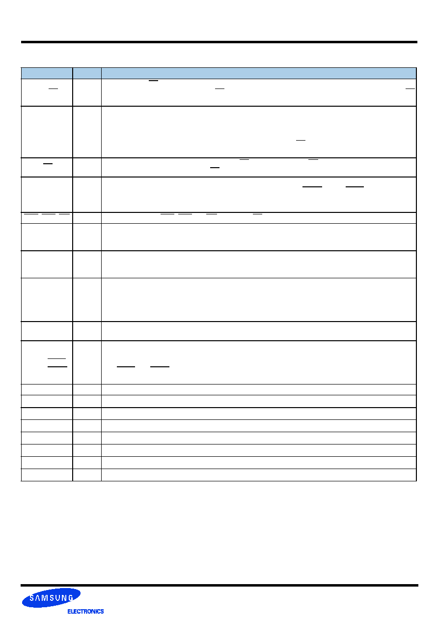
Symbol
Type
Function
CK, CK
Input
Clock: CK and CK are differential clock inputs. CMD, ADD inputs are sampled on the crossing of the posi-
tive edge of CK and negative edge of CK. Output (read) data is referenced to the crossings of CK and CK
(both directions of crossing).
CKE
Input
Clock Enable: CKE HIGH activates, and CKE Low deactivates, internal clock signals and device input
buffers and output drivers. Taking CKE Low provides Precharge Power-Down and Self Refresh operation
(all banks idle), or Active Power-Down (row Active in any bank). CKE is synchronous for power down entry
and exit, and for self refresh entry. CKE is asynchronous for self refresh exit. CKE must be maintained high
throughout read and write accesses. Input buffers, excluding CK, CK and CKE are disabled during power-
down. Input buffers, excluding CKE, are disabled during self refresh.
CS
Input
Chip Select: All commands are masked when CS is registered HIGH. CS provides for external bank selec-
tion on systems with multiple banks. CS is considered part of the command code.
ODT
Input
On Die Termination: ODT (registered HIGH) enables termination resistance internal to the gDDR2
SDRAM. When enabled, ODT is only applied to each DQ, UDQS/UDQS, LDQS/LDQS, UDM, and LDM
signal for x16 configurations. The ODT pin will be ignored if the Extended Mode Register (EMRS) is pro-
grammed to disable ODT.
RAS, CAS, WE
Input
Command Inputs: RAS, CAS and WE (along with CS) define the command being entered.
(L)UDM
Input
Input Data Mask: DM is an input mask signal for write data. Input data is masked when DM is sampled
HIGH coincident with that input data during a Write access. DM is sampled on both edges of DQS.
Although DM pins are input only, the DM loading matches the DQ and DQS loading.
BA0 - BA1
Input
Bank Address Inputs: BA0 and BA1 define to which bank an Actove, Read, Write or Precharge command
is being applied. BA0 also determines if the mode register or extended mode register is to be accessed dur-
ing a MRS or EMRS cycle.
A0 - A12
Input
Address Inputs: Provided the row address for Active commands and the column address and Auto Pre-
charge bit for Read/Write commands to select one location out of the memory array in the respective bank.
A10 is sampled during a Precharge command to determine whether the Precharge applies to one bank
(A10 LOW) or all banks (A10 HIGH). If only one bank is to be precharged, the bank is selected by BA0,
BA1. The address inputs also provide the op-code during Mode Register Set commands.
DQ
Input/
Output
Data Input/ Output: Bi-directional data bus.
LDQS,(LDQS)
UDQS,(UDQS)
Input/
Output
Data Strobe: output with read data, input with write data. Edge-aligned with read data, centered in write
data. LDQS corresponds to the data on DQ0-DQ7; UDQS corresponds to the data on DQ8-DQ15. The data
strobes LDQS and UDQS may be used in single ended mode or paired with optional complementary sig-
nals LDQS and UDQS to provide differential pair signaling to the system during both reads and writes. An
EMRS(1) control bit enables or disables all complementary data strobe signals.
NC/RFU
No Connect: No internal electrical connection is present.
V
DDQ
Supply DQ Power Supply: 1.8V � 0.1V
V
SSQ
Supply DQ Ground
V
DDL
Supply DLL Power Supply: 1.8V � 0.1V
V
SSL
Supply DLL Ground
V
DD
Supply Power Supply: 1.8V � 0.1V
V
SS
Supply Ground
V
REF
Supply Reference voltage
6.0 INPUT/OUTPUT FUNCTIONAL DESCRIPTION
- 7 -
Rev 1.5 Oct. 2005
512M gDDR2 SDRAM
K4N51163QC-ZC
Note :
1. Stresses greater than those listed under "Absolute Maximum Ratings" may cause permanent damage to the device. This is a stress rating only and
functional operation of the device at these or any other conditions above those indicated in the operational sections of this specification is not implied.
Exposure to absolute maximum rating conditions for extended periods may affect reliability.
2. Storage Temperature is the case surface temperature on the center/top side of the DRAM. For the measurement conditions, please refer to JESD51-
2 standard.
Symbol
Parameter
Rating
Units
Notes
VDD
Voltage on VDD pin relative to Vss
- 1.0 V ~ 2.3 V
V
1
VDDQ
Voltage on VDDQ pin relative to Vss
- 0.5 V ~ 2.3 V
V
1
VDDL
Voltage on VDDL pin relative to Vss
- 0.5 V ~ 2.3 V
V
1
V
IN,
V
OUT
Voltage on any pin relative to Vss
- 0.5 V ~ 2.3 V
V
1
T
STG
Storage Temperature
-55 to +100
�C 1,
2
Note : There is no specific device VDD supply voltage requirement for SSTL-1.8 compliance. However under all conditions VDDQ must be less than or
equal to VDD.
1. The value of VREF may be selected by the user to provide optimum noise margin in the system. Typically the value of VREF is expected to be about
0.5 x VDDQ of the transmitting device and VREF is expected to track variations in VDDQ.
2. Peak to peak AC noise on VREF may not exceed +/-2% VREF(DC).
3. VTT of transmitting device must track VREF of receiving device.
4. AC parameters are measured with VDD, VDDQ and VDDDL tied together.
Symbol
Parameter
Rating
Units
Notes
Min.
Typ.
Max.
VDD
Supply Voltage
1.7
1.8
1.9
V
VDDL
Supply Voltage for DLL
1.7
1.8
1.9
V
4
VDDQ
Supply Voltage for Output
1.7
1.8
1.9
V
4
VREF
Input Reference Voltage
0.49*VDDQ
0.50*VDDQ
0.51*VDDQ
mV
1,2
VTT
Termination Voltage
VREF-0.04
VREF
VREF+0.04
V
3
8.0 AC & DC OPERATING CONDITIONS
8.1 Recommended DC Operating Conditions (SSTL - 1.8)
Note :
1. Operating Temperature is the case surface temperature on the center/top side of the DRAM. For the measurement conditions, please refer to
JESD51.2 standard.
2. At 0 - 85
�C, operation temperature range are the temperature which all DRAM specification will be supported.
3. At 85 - 95
�C operation temperature range, doubling refresh commands in frequency to a 32ms period ( tREFI=3.9 us ) is required, and to enter to self
refresh mode at this temperature range, an EMRS command is required to change internal refresh rate.
Symbol
Parameter
Rating
Units
Note
TOPER
Operating Temperature
0 to 95
�C
1, 2, 3
8.2
Operating Temperature Condition
Input DC Logic Level
Input AC Logic Level
Symbol
Parameter
Min.
Max.
Units
Note
V
IH
(DC)
DC input logic high
V
REF
+ 0.125
V
DDQ
+ 0.3
V
V
IL
(DC)
DC input logic low
V
DDQ
- 0.3
V
REF
- 0.125
V
Symbol
Parameter
Min.
Max.
Units
Note
V
IH
(AC)
AC input logic high
V
REF
+ 0.250
-
V
V
IL
(AC)
AC input logic low
-
V
REF
- 0.250
V
8.3 Input DC & AC Logic Level
7.0 ABSOLUTE MAXIMUM DC RATINGS
- 8 -
Rev 1.5 Oct. 2005
512M gDDR2 SDRAM
K4N51163QC-ZC
Note :
1. Input waveform timing is referenced to the input signal crossing through the V
IH/IL
(AC)
level applied to the device under test.
2. The input signal minimum slew rate is to be maintained over the range from V
REF
to V
IH
(AC) min for rising edges and the range from V
REF
to V
IL
(AC)
max for falling edges as shown in the below figure.
3. AC timings are referenced with input waveforms switching from V
IL
(AC) to V
IH
(AC) on the positive transitions and V
IH
(AC) to V
IL
(AC) on the negative
transitions.
Symbol
Condition
Value
Units
Note
V
REF
Input reference voltage
0.5 * V
DDQ
V
1
V
SWING(MAX)
Input signal maximum peak to peak swing
1.0
V
1
SLEW
Input signal minimum slew rate
1.0
V/ns
2, 3
V
DDQ
V
IH
(AC) min
V
IH
(DC) min
V
REF
V
IL
(DC) max
V
IL
(AC) max
V
SS
< AC Input Test Signal Waveform >
V
SWING(MAX)
delta TR
delta TF
V
REF
- V
IL
(AC) max
delta TF
Falling Slew =
Rising Slew =
V
IH
(AC) min - V
REF
delta TR
V
DDQ
Crossing point
V
SSQ
V
TR
V
CP
V
ID
V
IX or
V
OX
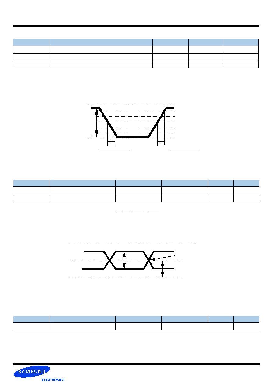
Note :
1. VID(AC) specifies the input differential voltage |VTR -VCP | required for switching, where VTR is the true input signal (such as CK, DQS, LDQS or
UDQS) and VCP is the complementary input signal (such as CK, DQS, LDQS or UDQS). The minimum value is equal to VIH(AC) - VIL(AC).
2. The typical value of VIX(AC) is expected to be about 0.5 * VDDQ of the transmitting device and VIX(AC) is expected to track variations in VDDQ .
VIX(AC) indicates the voltage at which differential input signals must cross.
Symbol
Parameter
Min.
Max.
Units
Note
V
ID
(AC)
AC differential input voltage
0.5
V
DDQ
+ 0.6
V
1
V
IX
(AC)
AC differential cross point voltage
0.5 * V
DDQ
- 0.175
0.5 * V
DDQ
+ 0.175
V
2
8.5 Differential input AC logic Level
Note :
1. The typical value of VOX(AC) is expected to be about 0.5 * VDDQ of the transmitting device and VOX(AC) is expected to track variations in VDDQ .
VOX(AC) indicates the voltage at which differential output signals must cross.
Symbol
Parameter
Min.
Max.
Units
Note
V
OX
(AC)
AC differential cross point voltage
0.5 * V
DDQ
- 0.125
0.5 * V
DDQ
+ 0.125
V
1
8.6 Differential AC output parameters
< Differential signal levels >
8.4 AC Input Test Conditions
- 9 -
Rev 1.5 Oct. 2005
512M gDDR2 SDRAM
K4N51163QC-ZC
Notes:
1. Absolute Specifications (0�C
T
CASE
+95�C; VDD = +1.8V �0.1V, VDDQ = +1.8V �0.1V)
2. Impedance measurement condition for output source dc current: VDDQ = 1.7V; VOUT = 1420mV; (VOUT-VDDQ)/Ioh must be less than 23.4 ohms for
values of VOUT between VDDQ and VDDQ-280mV. Impedance measurement condition for output sink dc current: VDDQ = 1.7V; VOUT = 280mV;
VOUT/Iol must be less than 23.4 ohms for values of VOUT between 0V and 280mV.
3. Mismatch is absolute value between pull-up and pull-dn, both are measured at same temperature and voltage.
4. Slew rate measured from V
IL
(AC) to V
IH
(AC).
5. The absolute value of the slew rate as measured from DC to DC is equal to or greater than the slew rate as measured from AC to AC. This is guaran-
teed by design and characterization.
6. This represents the step size when the OCD is near 18 ohms at nominal conditions across all process and represents only the DRAM uncertainty.
Output slew rate load :
7. DRAM output slew rate specification applies to 533Mb/sec/pin, 667Mb/sec/pin, 800Mb/sec/pin, 900Mbps/sec/pin and
1000Mbps/sec/pin speed bins.
8. Timing skew due to DRAM output slew rate mis-match between DQS / DQS and associated DQs is included in tDQSQ and tQHS
specification.
25 ohms
VTT
Output
(VOUT)
Reference
Point
Description
Parameter
Min
Nom
Max
Unit
Note
Output impedance
Normal 18ohms
See full strength default driver characteristics
ohms
1,2
Output impedance step size for
OCD calibration
0
1.5
ohms
6
Pull-up and pull-down mismatch
0
4
ohms
1,2,3
Output slew rate
Sout
1.5
5
V/ns
1,4,5,6,7,8
(Recommended operating conditions unless otherwise noted, 0
�C Tc 85�C )
Note :
1. Measured with outputs open and ODT off
Parameter
Symbol
Test Condition
Version
Unit
-25
-2A
-33
-36
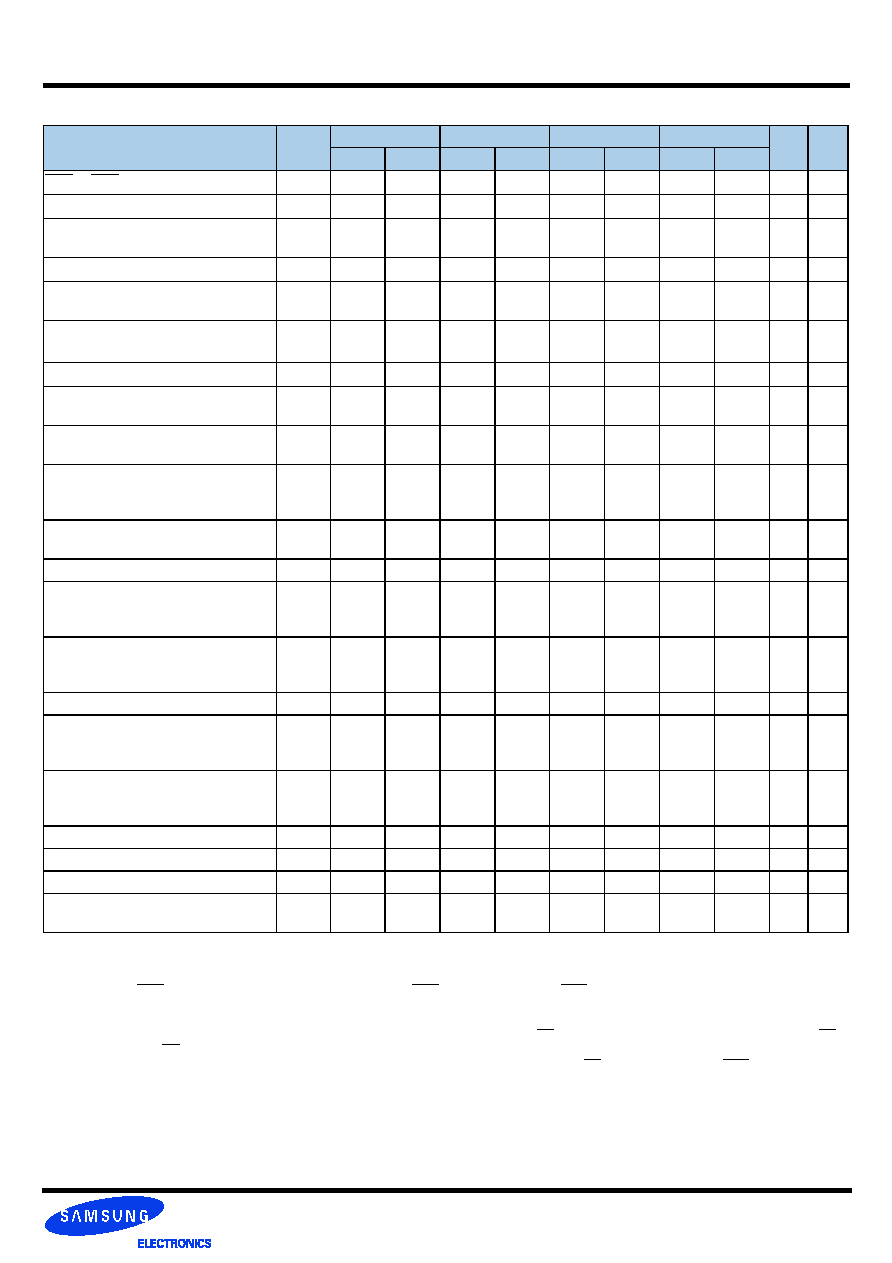
Operating Current
(One Bank Active)
ICC1
Burst Length=4 tRC
tRC(min). IOL=0mA, tCC= tCC(min).
DQ,DM,DQS inputs changing twice per clock cycle. Address
and control inputs changing once per clock cycle
TBD
140
TBD
130
mA
Precharge Standby Current
in Power-down mode
ICC2P
CKE
VIL(max), tCC= tCC(min)
TBD
10
mA
Precharge Standby Current
in Non Power-down mode
ICC2N
CKE
VIH(min), CS VIH(min),tCC= tCC(min)
Address and control inputs changing once per clock cycle
TBD
40
TBD
35
mA
Active Standby Current
power-down mode
ICC3P
CKE
VIL(max), tCC=
tCC(min)
Fast PDN Exit MRS(12) =
0mA
TBD
30
TBD
25
mA
Slow PDN Exit MRS(12) =
1mA
TBD
12
TBD
12
Active Standby Current in
in Non Power-down mode
ICC3N
CKE
VIH(min), CS VIH(min), tCC= tCC(min) DQ,DM,DQS
inputs changing twice per clock cycle. Address and control
inputs changing once per clock cycle
TBD
60
TBD
55
mA
Operating Current
( Burst Mode)
ICC4
IOL=0mA ,tCC= tCC(min),
Page Burst, All Banks activated. DQ,DM,DQS inputs changing
twice per clock cycle. Address and control inputs changing
once per clock.
TBD
200
TBD
170
mA
Refresh Current
ICC5
tRC
tRFC
TBD
160
TBD
165
mA
Self Refresh Current
ICC6
CKE
0.2V
TBD
8
TBD
8
mA
Operating Current
(4Bank interleaving)
ICC7
Burst Length=4 tRC
tRC(min). IOL=0mA, tCC= tCC(min).
DQ,DM,DQS inputs changing twice per clock cycle. Address
and control inputs changing once per clock cycle
TBD
350
TBD
320
mA
8.8 DC characteristics
8.7 OCD default characteristics
- 10 -
Rev 1.5 Oct. 2005
512M gDDR2 SDRAM
K4N51163QC-ZC
Parameter
Symbol
- 36
-33
- 2A
- 25
Units
Min
Max
Min
Max
Min
Max
Min
Max
Input capacitance, CK and CK
CCK
1.0
2.0
1.0
2.0
1.0
2.0
1.0
2.0
pF
Input capacitance delta, CK and CK
CDCK
x
0.25
x
0.25
x
0.25
x
0.25
pF
Input capacitance, all other input-only pins
CI
1.0
2.0
1.0
2.0
1.0
2.0
1.0
1.75
pF
Input capacitance delta, all other input-only pins
CDI
x
0.25
x
0.25
x
0.25
x
0.25
pF
Input/output capacitance, DQ, DM, DQS, DQS
CIO
2.5
4.0
2.5
4.0
2.5
3.5
2.5
3.5
pF
Input/output capacitance delta, DQ, DM, DQS, DQS
CDIO
x
0.5
x
0.5
x
0.5
x
0.5
pF
9.0 Electrical Characteristics & AC Timing for - 25/2A/33/36
(0
�C < T
CASE
< 95
�C; V
DDQ
= 1.8V + 0.1V; V
DD
= 1.8V + 0.1V)
SPEED
-25
- 2A
-33
- 36
Units
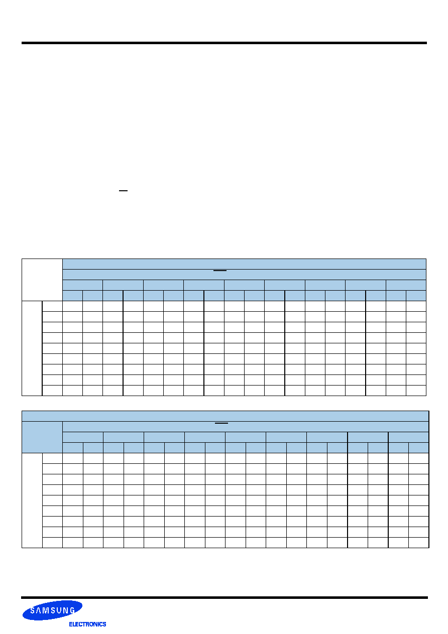
Bin (CL-tRCD-tRP)
5-5-5
5-5-5
5-5-5
4-4-4
Parameter
min
min
min
min
CAS LATENCY
5
5
5
4
tCK
tCK
2.5
2.86
3.3
3.6
ns
tRCD
5
5
5
4
tCK
tRP
5
5
5
4
tCK
tRC
21
18
18
15
tCK
tRAS
16
13
13
11
tCK
9.1 Refresh Parameters
Parameter
Symbol
512Mb
Units
Refresh to active/Refresh command time
tRFC
105
ns
Average periodic refresh interval
tREFI
0
�C T
CASE
85�C
7.8
�s
85
�C < T
CASE
95�C
3.9
�s
9.2 Speed Bins and CL, tRCD, tRP, tRC and tRAS
8.9 Input/Output capacitance
- 11 -
Rev 1.5 Oct. 2005
512M gDDR2 SDRAM
K4N51163QC-ZC
(Refer to notes for informations related to this table at the bottom)
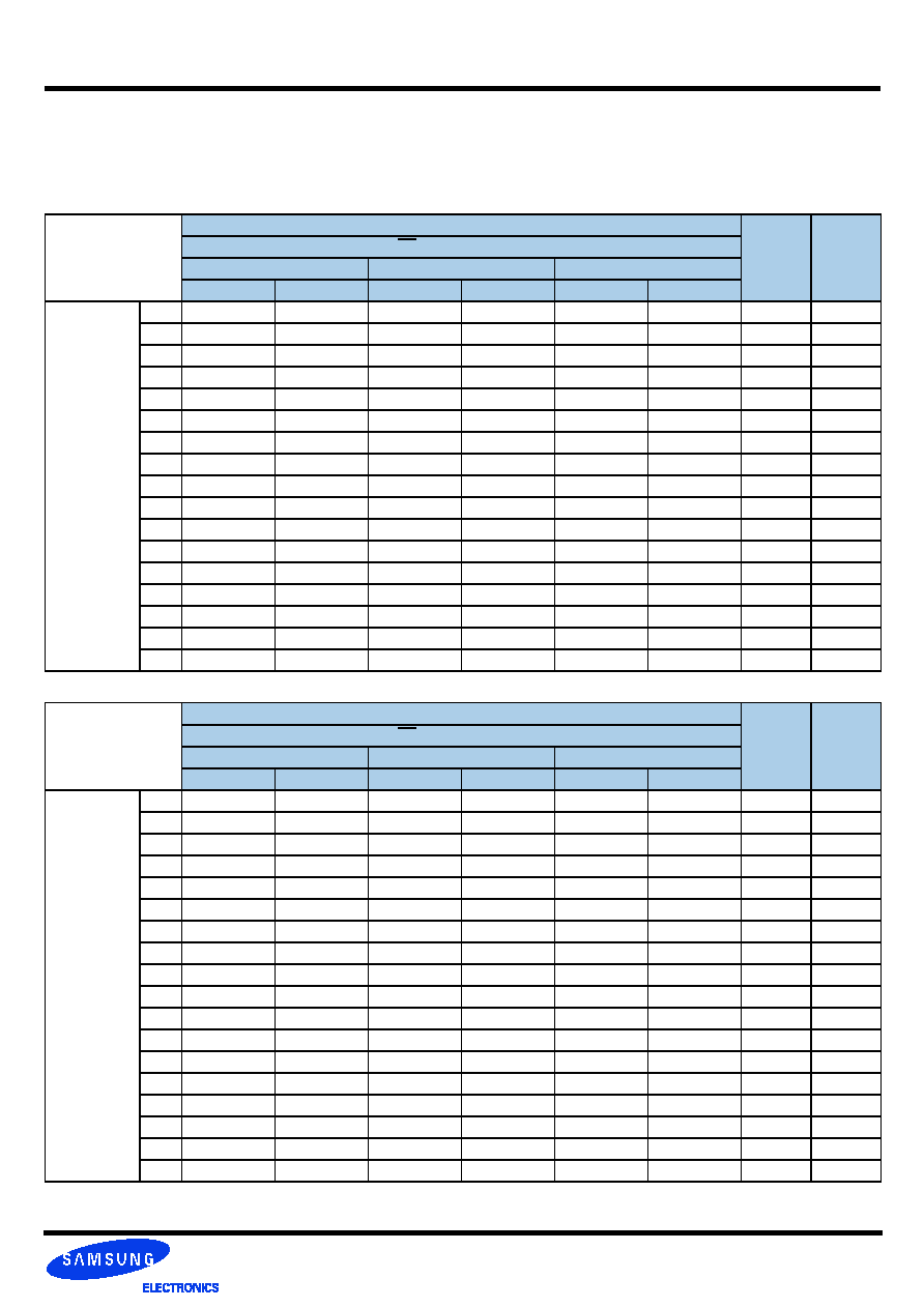
Parameter
Symbol
- 25
- 2A
- 33
- 36
Units Notes
min
max
min
max
min
max
min
max
DQ output access time from CK/CK
tAC
-400
+400
-450
+450
-470
+470
-500
+500
ps
DQS output access time from CK/CK
tDQSCK
-350
+350
-400
+400
-420
+420
-450
+450
ps
CK high-level width
tCH
0.45
0.55
0.45
0.55
0.45
0.55
0.45
0.55
tCK
CK low-level width
tCL
0.45
0.55
0.45
0.55
0.45
0.55
0.45
0.55
tCK
CK half period
tHP
min(tCL,
tCH)
x
min
(tCL,
tCH)
x
min
(tCL,
tCH)
x
min
(tCL,
tCH)
x
ps
20,21
Clock cycle time, CL= x
tCK
2500
8000
2.86
8.0
3.3
8.0
3.6
8.0
ns
24
DQ and DM input hold time
tDH
125
x
175
x
195
x
225
x
ps
15,16,
17
DQ and DM input setup time
tDS
50
x
50
x
70
x
100
x
ps
15,16,
17
Control & Address input pulse width for
each input
tIPW
0.6
x
0.6
x
0.6
x
0.6
x
tCK
DQ and DM input pulse width for each
input
tDIPW
0.35
x
0.35
x
0.35
x
0.35
x
tCK
Data-out high-impedance time from CK/
CK
tHZ
x
tAC
max
x
tAC
max
x
tAC
max
x
tAC
max
ps
DQS low-impedance time from CK/CK
tLZ
(DQS)
tAC
min
tAC
max
tAC
min
tAC
max
tAC
min
tAC
max
tAC
min
tAC
max
ps
27
DQ low-impedance time from CK/CK
tLZ(DQ) 2*tAC
min
tAC
max
2*tAC
min
tAC
max
2*tAC
min
tAC
max
2* tAC
min
tAC
max
ps
27
DQS-DQ skew for DQS and associated
DQ signals
tDQSQ
x
200
x
310
x
320
x
340
ps
22
DQ hold skew factor
tQHS
x
300
x
410
x
420
x
440
ps
21
DQ/DQS output hold time from DQS
tQH
tHP -
tQHS
x
tHP -
tQHS
x
tHP -
tQHS
x
tHP -
tQHS
x
ps
Write command to first DQS latching
transition
tDQSS
-0.25
0.25
WL
-0.25
WL
+0.25
WL
-0.25
WL
+0.25
WL
-0.25
WL
+0.25
tCK
DQS input high pulse width
tDQSH
0.35
x
0.35
x
0.35
x
0.35
x
tCK
DQS input low pulse width
tDQSL
0.35
x
0.35
x
0.35
x
0.35
x
tCK
DQS falling edge to CK setup time
tDSS
0.2
x
0.2
x
0.2
x
0.2
x
tCK
DQS falling edge hold time from CK
tDSH
0.2
x
0.2
x
0.2
x
0.2
x
tCK
Mode register set command cycle time
tMRD
2
x
2
x
2
x
2
x
tCK
Write postamble
tWPST
0.4
0.6
0.4
0.6
0.4
0.6
0.4
0.6
tCK
19
Write preamble
tWPRE
0.35
x
0.35
x
0.35
x
0.35
x
tCK
Address and control input hold time
tIH
250
x
325
x
345
x
375
x
ps
14,16,
18
Address and control input setup time
tIS
175
x
200
x
220
x
250
x
ps
14,16,
18
Read preamble
tRPRE
0.9
1.1
0.9
1.1
0.9
1.1
0.9
1.1
tCK
28
Read postamble
tRPST
0.4
0.6
0.4
0.6
0.4
0.6
0.4
0.6
tCK
28
Active to active command period for
1KB page size
products
tRRD
7.5
x
7.5
x
7.5
x
7.5
x
ns
12
Active to active command period for
2KB page size products
tRRD
10
x
10
x
10
x
10
x
ns
12
9.3 Timing Parameters by Speed Grade
- 12 -
Rev 1.5 Oct. 2005
512M gDDR2 SDRAM
K4N51163QC-ZC
Note : General notes, which may apply for all AC parameters
1. Slew Rate Measurement Levels
a. Output slew rate for falling and rising edges is measured between VTT - 250 mV and VTT + 250 mV for single ended signals. For differential signals
(e.g. DQS - DQS) output slew rate is measured between DQS - DQS = -500 mV and DQS - DQS = +500mV. Output slew rate is guaranteed by
design, but is not necessarily tested on each device.
b. Input slew rate for single ended signals is measured from dc-level to ac-level: from VREF - 125 mV to VREF + 250 mV for rising edges and from
VREF + 125 mV and VREF - 250 mV for falling edges. For differential signals (e.g. CK - CK) slew rate for rising edges is measured from CK - CK =
-250 mV to CK - CK = +500 mV (250mV to -500 mV for falling egdes).
c. VID is the magnitude of the difference between the input voltage on CK and the input voltage on CK, or between DQS and DQS for differential
strobe.
Parameter
Symbol
- 25
- 2A
-33
- 36
Units Notes
min
max
min
max
min
max
min
max
CAS to CAS command delay
tCCD
2
2
2
2
tCK
Write recovery time
tWR
6
x
5
x
5
x
4
x
tCK
Auto precharge write recovery + pre-
charge time
tDAL WR+tRP
x
tWR
+tRP
x
tWR
+tRP
x
tWR
+tRP
x
tCK
23
Internal write to read command delay
tWTR
3
3
x
3
x
2
x
tCK
Internal read to precharge command
delay
tRTP
3
3
3
2
tCK
11
Exit self refresh to a non-read com-
mand
tXSNR tRFC +
10
tRFC +
10
tRFC +
10
tRFC +
10
ns
Exit self refresh to a read command
tXSRD
200
200
200
200
tCK
Exit precharge power down to any
non-read command
tXP
2
x
2
x
2
x
2
x
tCK
Exit active power down to read com-
mand
tXARD
2
x
2
x
2
x
2
x
tCK
9
Exit active power down to read com-
mand
(Slow exit, Lower power)
tXARDS 8 - AL
6 - AL
6 - AL
6 - AL
tCK 9, 10
CKE minimum pulse width
(high and low pulse width)
tCKE
3
3
3
3
tCK
ODT turn-on delay
tAOND
2
2
2
2
2
2
2
2
tCK
ODT turn-on
tAON tAC(min)
tAC(max
)+0.7
tAC
(min)
tAC
(max)+0
.7
tAC
(min)
tAC
(max)+0
.7
tAC
(min)
tAC
(max)+1
ns 13, 25
ODT turn-on(Power-Down mode)
tAONPD
tAC(min)
+2
2tCK+tA
C(max)+
1
tAC
(min)+2
2tCK+
tAC(max
)+1
tAC
(min)+2
2tCK+
tAC(max
)+1
tAC
(min)+2
2tCK+tA
C(max)+
1
ns
ODT turn-off delay
tAOFD
2.5
2.5
2.5
2.5
2.5
2.5
2.5
2.5
tCK
ODT turn-off
tAOF tAC(min)
tAC(max
)+ 0.6
tAC
(min)
tAC
(max)+
0.6
tAC
(min)
tAC
(max)+
0.6
tAC
(min)
tAC
(max)+
0.6
ns
26
ODT turn-off (Power-Down mode)
tAOFPD
tAC(min)
+2
2.5tCK+
tAC(max
)+1
tAC(min)
+2
2.5tCK+t
AC(max)
+1
tAC(min)
+2
2.5tCK+t
AC(max)
+1
tAC(min)
+2
2.5tCK+
tAC(max
)+1
ns
ODT to power down entry latency
tANPD
3
3
3
3
tCK
ODT power down exit latency
tAXPD
8
8
8
8
tCK
OCD drive mode output delay
tOIT
0
12
0
12
0
12
0
12
ns
Minimum time clocks remains ON after
CKE asynchronously drops LOW
tDelay
tIS+tCK
+tIH
tIS+tCK
+tIH
tIS+tCK
+tIH
tIS+tCK
+tIH
ns
24
- 13 -
Rev 1.5 Oct. 2005
512M gDDR2 SDRAM
K4N51163QC-ZC
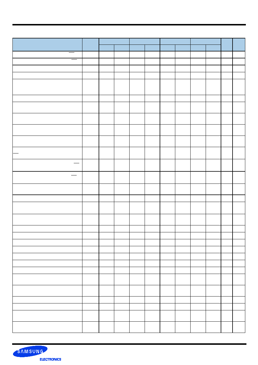
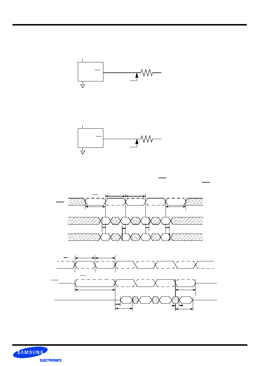
2. gDDR2 SDRAM AC timing reference load
Following figure represents the timing reference load used in defining the relevant timing parameters of the part. It is not intended to be either a precise
representation of the typical system environment or a depiction of the actual load presented by a production tester. System designers will use IBIS or
other simulation tools to correlate the timing reference load to a system environment. Manufacturers will correlate to their production test conditions (gen-
erally a coaxial transmission line terminated at the tester electronics).
The output timing reference voltage level for single ended signals is the crosspoint with VTT. The output timing reference voltage level for differential sig-
nals is the crosspoint of the true (e.g. DQS) and the complement (e.g. DQS) signal.
3. gDDR2 SDRAM output slew rate test load
Output slew rate is characterized under the test conditions as shown in the following figure.
4. Differential data strobe
gDDR2 SDRAM pin timings are specified for either single ended mode or differential mode depending on the setting of the EMRS "Enable DQS" mode
bit; timing advantages of differential mode are realized in system design. The method by which the gDDR2 SDRAM pin timings are measured is mode
dependent. In single ended mode, timing relationships are measured relative to the rising or falling edges of DQS crossing at VREF. In differential mode,
these timing relationships are measured relative to the crosspoint of DQS and its complement, DQS. This distinction in timing methods is guaranteed by
design and characterization. Note that when differential data strobe mode is disabled via the EMRS, the complementary pin, DQS, must be tied externally
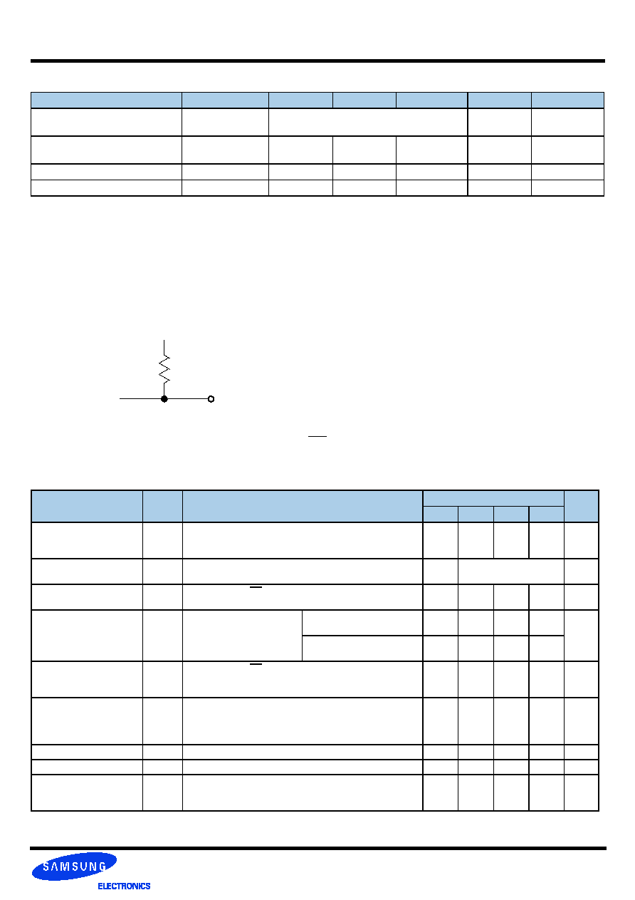
to VSS through a 20 ohm to 10 K ohm resisor to insure proper operation.
VDDQ
DUT
DQ
DQS
DQS
Output
V
TT
= V
DDQ
/2
25
Timing
reference
point
<AC Timing Reference Load>
VDDQ
DUT
DQ
DQS, DQS
Output
V
TT
= V
DDQ
/2
25
Test point
<Slew Rate Test Load>
t
DS
t
DS
t
DH
t
WPRE
t
WPST
t
DQSH
t
DQSL
DQS
DQS
D
DMin
DQS/
DQ
DM
t
DH
<Data input (write) timing>
DMin
DMin
DMin
D
D
D
DQS
V
IL
(ac)
V
IH
(ac)
V
IL
(ac)
V
IH
(ac)
V
IL
(dc)
V
IH
(dc)
V
IL
(dc)
V
IH
(dc)
t
CH
t
CL
CK
CK
CK/CK
DQS/DQS
DQ
DQS
DQS
t
RPST
Q
t
RPRE
t
DQSQmax
t
QH
t
QH
t
DQSQmax
<Data output (read) timing>
Q
Q
Q
- 14 -
Rev 1.5 Oct. 2005
512M gDDR2 SDRAM
K4N51163QC-ZC
5. AC timings are for linear signal transitions.
6. These parameters guarantee device behavior, but they are not necessarily tested on each device.
They may be guaranteed by device design or tester correlation.
7. All voltages are referenced to VSS.
8. Tests for AC timing, IDD, and electrical (AC and DC) characteristics, may be conducted at nominal reference/supply voltage levels, but the related
specifications and device operation are guaranteed for the full voltage range specified.
: Specific Notes for dedicated AC parameters
9. User can choose which active power down exit timing to use via MRS(bit 12). tXARD is expected to be used for fast active power down exit timing.
tXARDS is expected to be used for slow active power down exit timing.
10. AL = Additive Latency
11. This is a minimum requirement. Minimum read to precharge timing is AL + BL/2 providing the tRTP and tRAS(min) have been satisfied.
12. A minimum of two clocks (2 * tCK) is required irrespective of operating frequency
13. Timings are guaranteed with command/address input slew rate of 1.0 V/ns.
14. These parameters guarantee device behavior, but they are not necessarily tested on each device. They may be guaranteed by device design or
tester correlation.
15. Timings are guaranteed with data, mask, and (DQS in singled ended mode) input slew rate of 1.0 V/ns.
16. Timings are guaranteed with CK/CK differential slew rate of 2.0 V/ns. Timings are guaranteed for DQS signals with a differential slew rate of 2.0 V/ns
in differential strobe mode and a slew rate of 1V/ns in single ended mode.
17. tDS and tDH (data setup and hold) derating
1) Input waveform timing is referenced from the input signal crossing at the V
IH
(AC) level for a rising signal and V
IL
(AC) for a falling signal applied to
the device under test.
2) Input waveform timing is referenced from the input signal crossing at the V
IH
(DC) level for a rising signal and V
IL
(DC) for a falling signal applied to
the device under test.
For all input signals the total tDS (setup time) and tDH(hold time) required is calculated by adding the datasheet tDS(base) and tDH(base) value to the
delta tDS and delta tDH derating value respectively. Example : tDS (total setup time) = tDS(base) + delta tDS.
tDS, tDH Derating Values of gDDR2-550 (ALL units in `ps', Note 1 applies to entire Table)
DQS,DQS Differential Slew Rate
4.0 V/ns
3.0 V/ns
2.0 V/ns
1.8 V/ns
1.6 V/ns
1.4V/ns
1.2V/ns
1.0V/ns
0.8V/ns
tDS tDH tDS tDH tDS tDH tDS tDH tDS tDH tDS tDH tDS tDH tDS tDH tDS tDH
DQ
Slew
rate
V/ns
2.0
125
45
125
45
125
45
-
-
-
-
-
-
-
-
-
-
-
-
1.5
83
21
83
21
83
21
95
33
-
-
-
-
-
-
-
-
-
-
1.0
0
0
0
0
0
0
12
12
24
24
-
-
-
-
-
-
-
-
0.9
-
-
-11
-14
-11
-14
1
-2
13
10
25
22
-
-
-
-
-
-
0.8
-
-
-
-
-25
-31
-13
-19
-1
-7
11
5
23
17
-
-
-
-
0.7
-
-
-
-
-
-
-31
-42
-19
-30
-7
-18
5
-6
17
6
-
-
0.6
-
-
-
-
-
-
-
-
-43
-59
-31
-47
-19
-35
-7
-23
5
-11
0.5
-
-
-
-
-
-
-
-
-
-
-74
-89
-62
-77
-50
-65
-38
-53
0.4
-
-
-
-
-
-
-
-
-
-
-
-
-127
-140
-115
-128
-103
-116
tDS, tDH Derating Values for gDDR2-600/700/800 (ALL units in `ps', Note 1 applies to entire Table)
DQS,DQS Differential Slew Rate
4.0 V/ns
3.0 V/ns
2.0 V/ns
1.8 V/ns
1.6 V/ns
1.4V/ns
1.2V/ns
1.0V/ns
0.8V/ns
tDS tDH tDS tDH tDS tDH tDS tDH tDS tDH tDS tDH tDS tDH tDS tDH tDS tDH
DQ
Slew
rate
V/ns
2.0
100
45
100
45
100
45
-
-
-
-
-
-
-
-
-
-
-
-
1.5
67
21
67
21
67
21
79
33
-
-
-
-
-
-
-
-
-
-
1.0
0
0
0
0
0
0
12
12
24
24
-
-
-
-
-
-
-
-
0.9
-
-
-5
-14
-5
-14
7
-2
19
10
31
22
-
-
-
-
-
-
0.8
-
-
-
-
-13
-31
-1
-19
11
-7
23
5
35
17
-
-
-
-
0.7
-
-
-
-
-
-
-10
-42
2
-30
14
-18
26
-6
38
6
-
-
0.6
-
-
-
-
-
-
-
-
-10
-59
2
-47
14
-35
26
-23
38
-11
0.5
-
-
-
-
-
-
-
-
-
-
-24
-89
-12
-77
0
-65
12
-53
0.4
-
-
-
-
-
-
-
-
-
-
-
-
-52
-140
-40
-128
-28
-116
- 15 -
Rev 1.5 Oct. 2005
512M gDDR2 SDRAM
K4N51163QC-ZC
18. tIS and tIH (input setup and hold) derating
1) Input waveform timing is referenced from the input signal crossing at the V
IH
(AC) level for a rising signal and V
IL
(AC) for a falling signal applied to
the device under test.
2) Input waveform timing is referenced from the input signal crossing at the V
IH
(DC) level for a rising signal and V
IL
(DC) for a falling signal applied to
the device under test.
tIS, tIH Derating Values for gDDR2 550
Units
Notes
CK,CK Differential Slew Rate
2.0 V/ns
1.5 V/ns
1.0 V/ns
tIS
tIH
tIS
tIH
tIS
tIH
Command
/Adress Slew
rate(V/ns)
4.0
+187
+94
+217
+124
+247
+154
ps
1
3.5
+179
+89
+209
+119
+239
+149
ps
1
3.0
+167
+83
+197
+113
+227
+143
ps
1
2.5
+150
+75
+180
+105
+210
+135
ps
1
2.0
+125
+45
+155
+75
+185
+105
ps
1
1.5
+83
+21
+113
+51
+143
+81
ps
1
1.0
0
0
+30
+30
+60
+60
ps
1
0.9
-11
-14
+19
+16
+49
+46
ps
1
0.8
-25
-31
+5
-1
+35
+29
ps
1
0.7
-43
-54
-13
-24
+17
+6
ps
1
0.6
-67
-83
-37
-53
-7
-23
ps
1
0.5
-110
-125
-80
-95
-50
-65
ps
1
0.4
-175
-188
-145
-158
-115
-128
ps
1
0.3
-285
-292
-255
-262
-225
-232
ps
1
0.25
-350
-375
-320
-345
-290
-315
ps
1
0.2
-525
-500
-495
-470
-465
-440
ps
1
0.15
-800
-708
-770
-678
-740
-648
ps
1
tIS and tIH Derating Values for gDDR2-600, gDDR2-700, gDDR2-800
Units
Notes
CK,CK Differential Slew Rate
2.0 V/ns
1.5 V/ns
1.0 V/ns
tIS
tIH
tIS
tIH
tIS
tIH
Command
/Adress Slew
rate(V/ns)
4.0
+150
+94
+180
+124
+210
+154
ps
1
3.5
+143
+89
+173
+119
+203
+149
ps
1
3.0
+133
+83
+163
+113
+193
+143
ps
1
2.5
+120
+75
+150
+105
+180
+135
ps
1
2.0
+100
+45
+130
+75
+160
+105
ps
1
1.5
+67
+21
+97
+51
+127
+81
ps
1
1.0
0
0
+30
+30
+60
+60
ps
1
0.9
-5
-14
+25
+16
+55
+46
ps
1
0.8
-13
-31
+17
-1
+47
29
ps
1
0.7
-22
-54
+8
-24
+38
+6
ps
1
0.6
-34
-83
-4
-53
+26
-23
ps
1
0.5
-60
-125
-30
-95
0
-65
ps
1
0.4
-100
-188
-70
-158
-40
-128
ps
1
0.3
-168
-292
-138
-262
-108
-232
ps
1
0.25
-200
-375
-170
-345
-140
-315
ps
1
0.2
-325
-500
-295
-470
-265
-440
ps
1
0.15
-517
-708
-487
-678
-457
-648
ps
1
0.1
-1000
-1125
-970
-1095
-940
-1065
- 16 -
Rev 1.5 Oct. 2005
512M gDDR2 SDRAM
K4N51163QC-ZC
19. The maximum limit for this parameter is not a device limit. The device will operate with a greater value for this parameter, but system performance
(bus turnaround) will degrade accordingly.
20. MIN ( tCL, tCH) refers to the smaller of the actual clock low time and the actual clock high time as provided to the device (i.e. this value can be greater
than the minimum specification limits for tCL and tCH). For example, tCL and tCH are = 50% of the period, less the half period jitter ( tJIT(HP)) of the
clock source, and less the half period jitter due to crosstalk ( tJIT(crosstalk)) into the clock traces.
21. tQH = tHP � tQHS, where:
tHP = minimum half clock period for any given cycle and is defined by clock high or clock low ( tCH, tCL).
tQHS accounts for:
1) The pulse duration distortion of on-chip clock circuits; and
2) The worst case push-out of DQS on one transition followed by the worst case pull-in of DQ on the next transition, both of which are, separately,
due to data pin skew and output pattern effects, and p-channel to n-channel variation of the output drivers.
22. tDQSQ: Consists of data pin skew and output pattern effects, and p-channel to n-channel variation of the output drivers as well as output slew rate
mismatch between DQS / DQS and associated DQ in any given cycle.
23. tDAL = (nWR) + ( tRP/tCK) :
For each of the terms above, if not already an integer, round to the next highest integer. tCK refers to the application clock period. nWR refers to the
tWR parameter stored in the MRS.
Example: For gDDR533 at t CK = 3.75 ns with tWR programmed to 4 clocks. tDAL = 4 + (15 ns / 3.75 ns) clocks =4 +(4)clocks=8clocks.
24. The clock frequency is allowed to change during self�refresh mode or precharge power-down mode. In case of clock frequency change during pre-
charge power-down, a specific procedure is required as described in gDDR2 device operation
25. ODT turn on time min is when the device leaves high impedance and ODT resistance begins to turn on.
ODT turn on time max is when the ODT resistance is fully on. Both are measured from tAOND.
26. ODT turn off time min is when the device starts to turn off ODT resistance.
ODT turn off time max is when the bus is in high impedance. Both are measured from tAOFD.
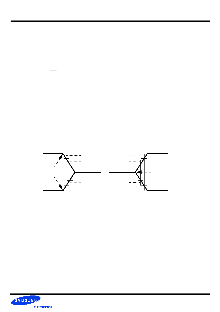
27. tHZ and tLZ transitions occur in the same access time as valid data transitions. These parameters are referenced to a specific voltage level which
specifies when the device output is no longer driving (tHZ), or begins driving (tLZ) . Following figure shows a method to calculate the point when
device is no longer driving (tHZ), or begins driving (tLZ) by measuring the signal at two different voltages. The actual voltage measurement points are
not critical as long as the calculation is consistent.
28. tRPST end point and tRPRE begin point are not referenced to a specific voltage level but specify when the device output is no longer driving (tRPST),
or begins driving (tRPRE). Following figure shows a method to calculate these points when the device is no longer driving (tRPST), or begins driving
(tRPRE) by measuring the signal at two different voltages. The actual voltage measurement points are not critical as long as the calculation is consis-
tent. These notes are referenced to the "Timing parameters by speed grade" tables for gDDR2-550/600/700 and gDDR2-800.
tHZ
tRPST end point
T1
T2
VOH + x mV
VOH + 2x mV
VOL + 2x mV
VOL + x mV
tLZ
tRPRE begin point
T2
T1
VTT + 2x mV
VTT + x mV
VTT - x mV
VTT - 2x mV
tLZ,tRPRE begin point = 2*T1-T2
tHZ,tRPST end point = 2*T1-T2
<Test method for tLZ, tHZ, tRPRE and tRPST>

- 17 -
Rev 1.5 Oct. 2005
512M gDDR2 SDRAM
K4N51163QC-ZC
29. Input waveform timing with differential data strobe enabled MR[bit10]=0, is referenced from the input signal crossing at the V
IH(ac)
level to the differ-
ential data strobe crosspoint for a rising signal, and from the input signal crossing at the V
IL(ac)
level to the differential data strobe crosspoint for a
falling signal applied to the device under test.
30. Input waveform timing with differential data strobe enabled MR[bit10]=0, is referenced from the input signal crossing at the V
IH(dc)
level to the differ-
ential data strobe crosspoint for a rising signal and V
IL(dc)
to the differential data strobe crosspoint for a falling signal applied to the device under
test.
Differential Input waveform timing
tDS
V
DDQ
V
IH
(AC) min
V
IH
(DC) min
V
REF
V
IL
(DC) max
V
IL
(AC) max
V
SS
DQS
DQS
tDH
tDS
tDH
<Data setup/hold timing>
3
3. tWTR is at lease two clocks (2 * tCK) independent of operation frequency.
34. Input waveform timing with single-ended data strobe enabled MR[bit10] = 1, is referenced from the input signal crossing at the VIH(ac) level to the sin-
gle-ended data strobe crossing VIH/L(dc) at the start of its transition for a rising signal, and from the input signal crossing at the VIL(ac) level to the
single-ended data strobe crossing VIH/L(dc) at the start of its transition for a falling signal applied to the device under test. The DQS signal must be
monotonic between Vil(dc)max and Vih(dc)min.
35. Input waveform timing with single-ended data strobe enabled MR[bit10] = 1, is referenced from the input signal crossing at the VIH(dc) level to the sin-
gle-ended data strobe crossing VIH/L(ac) at the end of its transition for a rising signal, and from the input signal crossing at the VIL(dc) level to the sin-
gle-ended data strobe crossing VIH/L(ac) at the end of its transition for a falling signal applied to the device under test. The DQS signal must be
monotonic between Vil(dc)max and Vih(dc)min.
36. tCKEmin of 3 clocks means CKE must be registered on three consecutive positive clock edges. CKE must remain at the valid input level the entire
time it takes to achieve the 3 clocks of registeration. Thus, after any cKE transition, CKE may not transitioin from its valid level during the time period
of tIS + 2*tCK + tIH.
31. Input waveform timing is referenced from the input signal crossing at the VIH(ac) level for a rising signal and VIL(ac) for a falling signal applied to the
device under test.
32. Input waveform timing is referenced from the input signal crossing at the VIL(dc) level for a rising signal and VIH(dc) for a falling signal applied to the
device under test.
tIS
V
DDQ
V
IH
(AC) min
V
IH
(DC) min
V
REF
V
IL
(DC) max
V
IL
(AC) max
V
SS
CK
CK
tIH
tIS
tIH
<Input setup/hold timing>

- 18 -
Rev 1.5 Oct. 2005
512M gDDR2 SDRAM
K4N51163QC-ZC
Device Operation &
Timing Diagram
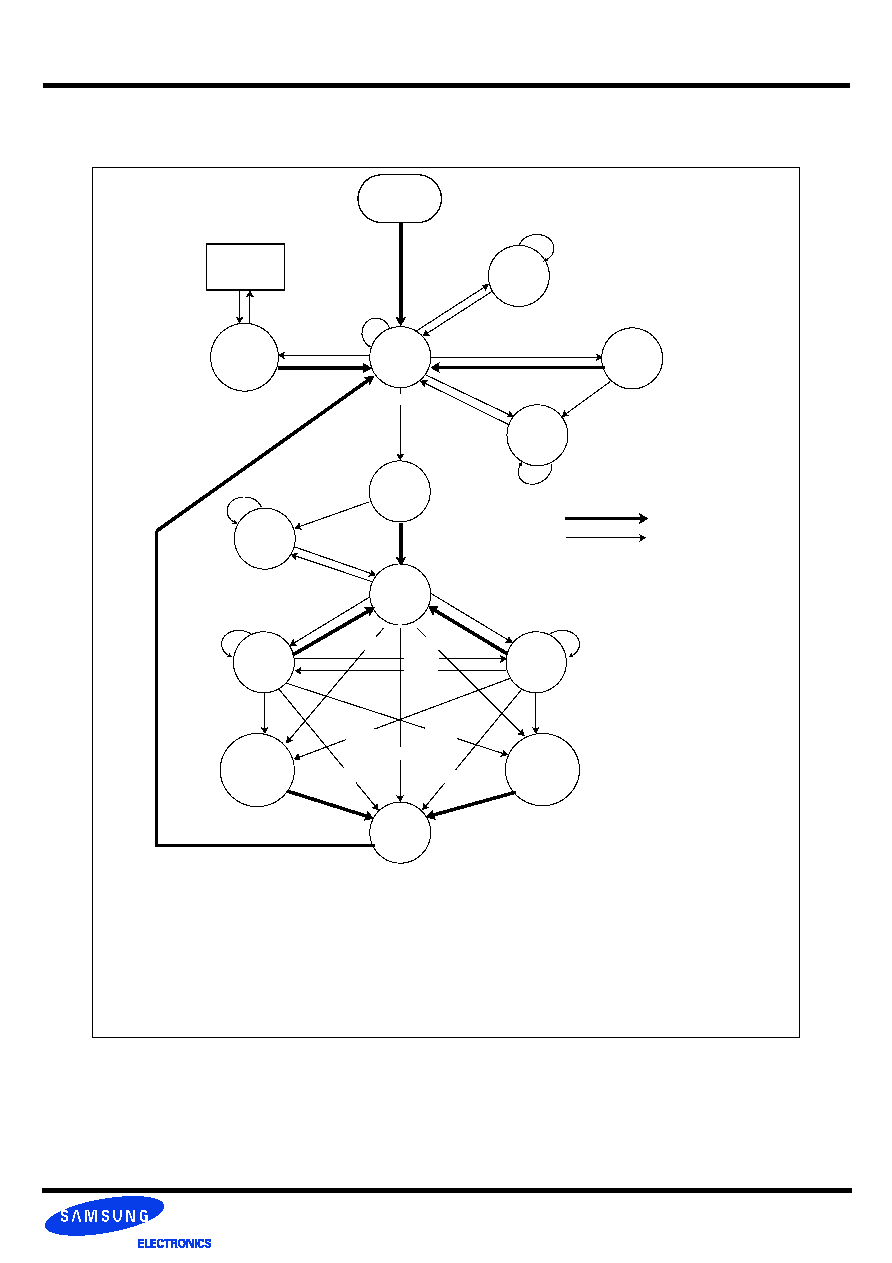
- 19 -
Rev 1.5 Oct. 2005
512M gDDR2 SDRAM
K4N51163QC-ZC
Functional Description
Simplified State Diagram
Self
Idle
Setting
EMRS
Bank
Precharging
Power
Writing
ACT
RDA
Read
SRF
REF
CKEL
(E)MRS
CKEH
CKEH
CKEL
Write
Automatic Sequence
Command Sequence
RDA
WRA
Read
PR, PRA
PR
Refreshing
Refreshing
Down
Power
Down
Active
with
RDA
Reading
with
WRA
Active
Precharge
Reading
Writing
PR(A) = Precharge (All)
(E)MRS = (Extended) Mode Register Set
SRF = Enter Self Refresh
REF = Refresh
CKEL = CKE low, enter Power Down
CKEH = CKE high, exit Power Down, exit Self Refresh
ACT = Activate
WR(A) = Write (with Autoprecharge)
RD(A) = Read (with Autoprecharge)
All banks
precharged
Activating
CKEH
Read
Write
CKEL
MRS
CKEL
Sequence
Initialization
OCD
calibration
CKEL
CKEL
CKEL
Autoprecharge
Autoprecharge
PR, PRA
PR, PRA
Write
WRA
Note : Use caution with this diagram. It is indented to provide a floorplan of the possible state transitions and the commands to control
them, not all details. In particular situations involving more than one bank, enabling/disabling on-die termination, Power Down entry/
exit - among other things - are not captured in full detail.

- 20 -
Rev 1.5 Oct. 2005
512M gDDR2 SDRAM
K4N51163QC-ZC
gDDR2 SDRAMs must be powered up and initialized in a predefined manner. Operational procedures other than those specified may
result in undefined operation.
Power-up and Initialization Sequence
The following sequence is required for POWER UP and Initialization.
1. Apply power and attempt to maintain CKE below 0.2*VDDQ and ODT
*1
at a low state (all other inputs may be undefined.) The
power voltage ramps are without any slope reversal, ramp time must be no greater than 20mS; and during the ramp,
VDD>VDDL>VDDQ and VDD-VDDQ<0.3 volts.
- VDD
*2
, VDDL
*2
and VDDQ are driven from a single power converter output, AND
- VTT is limited to 0.95 V max, AND
-
Vref tracks VDDQ/2.
or
- Apply VDD
*2
before or at the same time as VDDL.
- Apply VDDL
*2
before or at the same time as VDDQ.
-
Apply VDDQ before or at the same time as VTT & V
REF
.
at least one of these two sets of conditions must be met.
2. Start clock and maintain stable condition.
3. For the minimum of 200
�s after stable power and clock(CK, CK), then apply NOP or deselect & take CKE high.
4. Wait minimum of 400ns then issue precharge all command. NOP or deselect applied during 400ns period.
5. Issue EMRS(2) command. (To issue EMRS(2) command, provide "Low" to BA0, "High" to BA1.)
6. Issue EMRS(3) command. (To issue EMRS(3) command, provide "High" to BA0 and BA1.)
7. Issue EMRS to enable DLL. (To issue "DLL Enable" command, provide "Low" to A0, "High" to BA0 and "Low" to BA1 and A12.)
8. Issue a Mode Register Set command for "DLL reset"
*2
.
(To issue DLL reset command, provide "High" to A8 and "Low" to BA0-1)
9. Issue precharge all command.
10. Issue 2 or more auto-refresh commands.
11. Issue a mode register set command with low to A8 to initialize device operation. (i.e. to program operating parameters without
resetting the DLL.
12. At least 200 clocks after step 8, execute OCD Calibration ( Off Chip Driver impedance adjustment ).
If OCD calibration is not used, EMRS OCD Default command (A9=A8= A7=1) followed by EMRS OCD Calibration Mode Exit com-
mand (A9=A8=A7=0) must be issued with other operating parameters of EMRS.
13. The gDDR2 SDRAM is now ready for normal operation.
*1) To guarantee ODT off, V
REF
must be valid and a low level must be applied to the ODT pin.
*2) If DC voltage level of V
DDL
or V
DD
is intentionally changed during normal operation, (for example, for the purpose of V
DD
corner test, or power
saving) "DLL Reset" must be executed.
Read and write accesses to the gDDR2 SDRAM are burst oriented; accesses start at a selected location and continue for a burst
length of four or eight in a programmed sequence. Accesses begin with the registration of an Active command, which is then followed by
a Read or Write command. The address bits registered coincident with the active command are used to select the bank and row to be
accessed (BA0, BA1 select the bank; A0-A12 select the row). The address bits registered coincident with the Read or Write command
are used to select the starting column location for the burst access and to determine if the auto precharge command is to be issued.
Prior to normal operation, the gDDR2 SDRAM must be initialized. The following sections provide detailed information covering device
initialization, register definition, command descriptions and device operation.
Power up and Initialization
Basic Functionality

- 21 -
Rev 1.5 Oct. 2005
512M gDDR2 SDRAM
K4N51163QC-ZC
For application flexibility, burst length, burst type, CAS latency, DLL reset function, write recovery time(tWR) are user defined variables
and must be programmed with a Mode Register Set (MRS) command. Additionally, DLL disable function, driver impedance, additive
CAS latency, ODT(On Die Termination), single-ended strobe, and OCD(off chip driver impedance adjustment) are also user defined
variables and must be programmed with an Extended Mode Register Set (EMRS) command. Contents of the Mode Register(MR) or
Extended Mode Registers(EMR(#)) can be altered by re-executing the MRS and EMRS Commands. If the user chooses to modify only
a subset of the MRS or EMRS variables, all variables must be redefined when the MRS or EMRS commands are issued.
MRS, EMRS and Reset DLL do not affect array contents, which means reinitialization including those can be executed any time after
power-up without affecting array contents.
Initialization Sequence after Power Up
/CK
CK
CKE
Command
PRE
ALL
PRE
ALL
EMRS
MRS
REF
REF
MRS
EMRS
EMRS
ANY
CMD
DLL
ENABLE
DLL
RESET
OCD
Default
OCD
CAL. MODE
EXIT
Follow OCD
Flowchart
400ns
tRFC
tRFC
tRP
tRP
tMRD
tMRD
tMRD
tOIT
min. 200 Cycle
NOP
ODT
tCL
tCH
tIS
V
IH(ac)
Programming the Mode Register

- 22 -
Rev 1.5 Oct. 2005
512M gDDR2 SDRAM
K4N51163QC-ZC
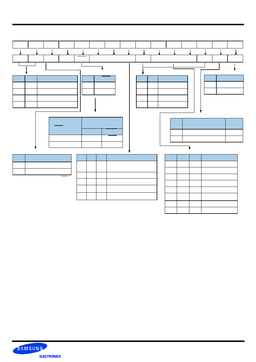
The mode register stores the data for controlling the various operating modes of gDDR2 SDRAM. It controls CAS latency, burst length,
burst sequence, test mode, DLL reset, tWR and various vendor specific options to make gDDR2 SDRAM useful for various applications.
The default value of the mode register is not defined, therefore the mode register must be written after power-up for proper operation.
The mode register is written by asserting low on CS, RAS, CAS, WE, BA0 and BA1, while controlling the state of address pins A0 ~
A15. The gDDR2 SDRAM should be in all bank precharge with CKE already high prior to writing into the mode register. The mode reg-
ister set command cycle time (tMRD) is required to complete the write operation to the mode register. The mode register contents can
be changed using the same command and clock cycle requirements during normal operation as long as all banks are in the precharge
state. The mode register is divided into various fields depending on functionality. Burst length is defined by A0 ~ A2 with options of 4 and
8 bit burst lengths. The burst length decodes are compatible with gDDR SDRAM. Burst address sequence type is defined by A3, CAS
latency is defined by A4 ~ A6. The gDDR2 doesn't support half clock latency mode. A7 is used for test mode. A8 is used for DLL reset.
A7 must be set to low for normal MRS operation. Write recovery time tWR is defined by A9 ~ A11. Refer to the table for specific codes.
*1 : WR(write recovery for autoprecharge) min is determined by tCK max and WR max is determined by tCK min. WR in clock cycles
is calculated by dividing tWR (in ns) by tCK (in ns) and rounding up a non-integer value to the next integer
(WR[cycles] = tWR(ns)/tCK(ns)). The mode register must be programmed to this value. This is also used with tRP to determine tDAL.
CAS Latency
A6
A5
A4
Latency
0
0
0
Reserved
0
0
1
Reserved
0
1
0
Reserved
0
1
1
3
1
0
0
4
1
0
1
5
1
1
0
6
1
1
1
Reserved
Burst Length
A2
A1
A0
Burst Length
0
1
0
4
0
1
1
8
Burst Type
A3
Type
0
Sequential
1
Interleave
BA
1
BA
0
A
12
A
11
A
10
A
9
A
8
A
7
A
6
A
5
A
4
A
3
A
2
A
1
A
0
BA1
BA0
MRS Mode
0
0
MRS
0
1
EMRS (1)
1
0
EMRS (2) : Reserved
1
1
EMRS (3) : Reserved
DLL
A8
DLL Reset
0
No
1
Yes
Test Mode
A7
mode
0
Normal
1
Test
0
0
PD
tWR
*1
DLL
TM
CAS Latency
BT
Burst Length
A12
Active Power
Down exit time
0
Fast exit (use tXARD)
1
Slow exit (use tXARDS)
Write Recovery for Auto Precharge
A11
A10
A9
MRS Select
0
0
0
Reserved
0
0
1
Reserved
0
1
0
3
0
1
1
4
1
0
0
5
1
0
1
Reserved
1
1
0
Reserved
1
1
1
Reserved
gDDR2 SDRAM Mode Register Set (MRS)
Address Bus
Mode Register

- 23 -
Rev 1.5 Oct. 2005
512M gDDR2 SDRAM
K4N51163QC-ZC
EMRS(1)
The extended mode register(1) stores the data for enabling or disabling the DLL, output driver strength, ODT value selection and addi-
tive latency. The default value of the extended mode register is not defined, therefore the extended mode register must be written after
power-up for proper operation. The extended mode register is written by asserting low on CS, RAS, CAS, WE and high on BA0, while
controlling the states of address pins A0 ~ A12. The gDDR2 SDRAM should be in all bank precharge with CKE already high prior to writ-
ing into the extended mode register. The mode register set command cycle time (tMRD) must be satisfied to complete the write opera-
tion to the extended mode register. Mode register contents can be changed using the same command and clock cycle requirements
during normal operation as long as all banks are in the precharge state. A0 is used for DLL enable or disable. A1 is used for enabling a
half strength data-output driver. A3~A5 determines the additive latency, A2 and A6 are used for ODT value selection, A7~A9 are used
for OCD control, A10 is used for DQS# disable.
DLL Enable/Disable
The DLL must be enabled for normal operation. DLL enable is required during power up initialization, and upon returning to normal oper-
ation after having the DLL disabled. The DLL is automatically disabled when entering self refresh operation and is automatically re-
enabled upon exit of self refresh operation. Any time the DLL is enabled (and subsequently reset), 200 clock cycles must occur before a
Read command can be issued to allow time for the internal clock to be synchronized with the external clock. Failing to wait for synchro-
nization to occur may result in a violation of the tAC or tDQSCK parameters.
EMRS(2)
The extended mode register(2) controls refresh related features. The default value of the extended mode register(2) is not defined,
therefore the extended mode register(2) must be written after power-up for proper operation. The extended mode register(2) is written
by asserting low on CS, RAS, CAS, WE, high on BA1 and low on BA0, while controlling the ststes of address pins A0 ~ A15. The gDDR2
SDRAM should be in all bank precharge with CKE already high prior to writing into the extended mode register(2). The mode register set
command cycle time (tMRD) must be satisfied to complete the write operation to the extended mode register(2). Mode register contents
can be changed using the same command and clock cycle requirements during normal operation as long as all banks are in the pre-
charge state.
gDDR2 SDRAM Extended Mode Register Set
- 24 -
Rev 1.5 Oct. 2005
512M gDDR2 SDRAM
K4N51163QC-ZC
EMRS (1) Programming
A0
DLL Enable
0
Enable
1
Disable
a. AL 5 option is available only for 256Mb gDDR2.
A5
A4
A3
Additive Latency
0
0
0
0
0
0
1
1
0
1
0
2
0
1
1
3
1
0
0
4
1
0
1
5
a
1
1
0
Reserved
1
1
1
Reserved
a: When Adjust mode is issued, AL from previously
set value must be applied.
b: After setting to default, OCD mode needs to be
exited by setting A9-A7 to 000. Refer to the follow-
ing 3.2.2.3 section for detailed information.
A9
A8
A7
OCD Calibration Program
0
0
0
OCD Calibration mode exit;
maintain setting
0
0
1
Drive(1)
0
1
0
Drive(0)
1
0
0
Adjust mode
a
1
1
1
OCD Calibration default
b
A1
Output Driver
Impedance Control
Driver
Size
0
Normal 100%
1
Weak
60%
A10
DQS
0
Enable
1
Disable
A6
A2
Rtt (
NOMINAL
)
0
0
ODT Disabled
0
1
75 ohm
1
0
150 ohm
1
1
50 ohm
BA1
BA0
MRS mode
0
0
MRS
0
1
EMRS(1)
1
0
EMRS(2): Reserved
1
1
EMRS(3): Reserved
a. Outputs disabled - DQs, DQSs, DQSs .
This feature is used in conjunction with
dimm IDD meaurements when IDDQ is
not desired to be included.
A12
Qoff (Optional)
a
0
Output buffer enabled
1
Output buffer disabled
A10
(DQS Enable)
Strobe Function
Matrix
DQS
DQS
0 (Enable)
DQS
DQS
1 (Disable)
DQS
Hi-z
BA1
BA0
A12
A11
A10
A9
A8
A7
A6
A5
A4
A3
A2
A1
A0
0
1
Qoff
0
DQS
OCD Program
Rtt
Additive Latency
Rtt
D.I.C
DLL

- 25 -
Rev 1.5 Oct. 2005
512M gDDR2 SDRAM
K4N51163QC-ZC
*1 : The rest bits in EMRS(2) is reserved for future use and all bits except A0, A1, A2, A7and BA0, BA1, must be programmed
to 0 when setting the mode register during initialization.
.
*2 : If PASR (Partial Array Self Refresh) is enabled, data located in areas of the array beyond the specified location will be
loast if self refresh is entered. Data integrity will be maintained if tREF conditions are met and no Self Refresh command
is issued. PASR is supported from the device of 90nm technology(512Mb C-die).
*1 : All bits in EMRS(3) except BA0 and BA1 are reserved for future use and must be programmed to 0 when setting the
mode register during initialization.
Address Field
Extended Mode Register(2)
BA1
BA0
MRS mode
0
0
MRS
0
1
EMRS(1)
1
0
EMRS(2)
1
1
EMRS(3): Reserved
A7
High Temperature Self-Refresh Rate Enable
1
Enable
0
Disable
A2
A1
A0 Partial Array Self Refresh for 4 Banks
0
0
0
Full array
0
0
1
Half Array(BA[1:0]=00&01)
0
1
0
Quarter Array(BA[1:0]=00)
0
1
1
Not defined
1
0
0
3/4 array(BA[1:0]=01, 10&11)
1
0
1
Half array(BA[1:0]=10&11)
1
1
0
Quarter array(BA[1:0]=11)
1
1
1
Not defined
BA1 BA0
A12
A11
A10
A9
A8
A7
A6
A5
A4
A3
A2
A1
A0
1
0
*1
0
*1
SRF
0
*1
PSAR
*2
Address Field
Extended Mode Register(3)
BA1 BA0
A12
A11
A10
A9
A8
A7
A6
A5
A4
A3
A2
A1
A0
1
1
0
*1
EMRS (2) Programming
EMRS (3) Programming : Reserved
*1
- 26 -
Rev 1.5 Oct. 2005
512M gDDR2 SDRAM
K4N51163QC-ZC
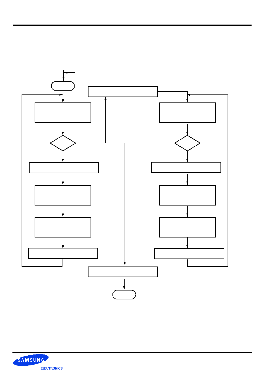
gDDR2 SDRAM supports driver calibration feature and the flow chart below is an example of sequence. Every calibration mode com-
mand should be followed by "OCD calibration mode exit" before any other command being issued. MRS should be set before entering
OCD impedance adjustment and ODT (On Die Termination) should be carefully controlled depending on system environment.
Start
EMRS: Drive(1)
DQ & DQS High; DQS Low
Test
EMRS :
Enter Adjust Mode
BL=4 code input to all DQs
Inc, Dec, or NOP
EMRS: Drive(0)
DQ & DQS Low; DQS High
Test
EMRS :
Enter Adjust Mode
BL=4 code input to all DQs
Inc, Dec, or NOP
EMRS: OCD calibration mode exit
End
ALL OK
ALL OK
Need Calibration
Need Calibration
EMRS: OCD calibration mode exit
EMRS: OCD calibration mode exit
EMRS: OCD calibration mode exit
EMRS: OCD calibration mode exit
EMRS: OCD calibration mode exit
MRS shoud be set before entering OCD impedance adjustment and ODT should be
carefully controlled depending on system environment
Off-Chip Driver (OCD) Impedance Adjustment

- 27 -
Rev 1.5 Oct. 2005
512M gDDR2 SDRAM
K4N51163QC-ZC
To adjust output driver impedance, controllers must issue the ADJUST EMRS command along with a 4bit burst code to gDDR2
SDRAM as in the following table. For this operation, Burst Length has to be set to BL = 4 via MRS command before activating OCD and
controllers must drive this burst code to all DQs at the same time. DT0 in the following table means all DQ bits at bit time 0, DT1 at bit
time 1, and so forth. The driver output impedance is adjusted for all gDDR2 SDRAM DQs simultaneously and after OCD calibration, all
DQs of a given gDDR2 SDRAM will be adjusted to the same driver strength setting. The maximum step count for adjustment is 16 and
when the limit is reached, further increment or decrement code has no effect. The default setting may be any step within the 16 step
range. When Adjust mode command is issued, AL from previously set value must be applied.
Extended Mode Register Set for OCD impedance adjustment
OCD impedance adjustment can be done using the following EMRS mode. In drive mode all outputs are driven out by gDDR2 SDRAM
and drive of DQS is dependent on EMRS bit enabling DQS operation. In Drive(1) mode, all DQ, DQS signals are driven high and all DQS
signals are driven low. In drive(0) mode, all DQ, DQS signals are driven low and all DQS signals are driven high. In adjust mode, BL = 4
of operation code data must be used. In case of OCD calibration default, output driver characteristics have a nominal impedance value
of 18 ohms during nominal temperature and voltage conditions. Output driver characteristics for OCD calibration default are specified in
section 6. OCD applies only to normal full strength output drive setting defined by EMRS(1) and if half strength is set, OCD default output
driver characteristics are not applicable. When OCD calibration adjust mode is used, OCD default output driver characteristics are not
applicable. After OCD calibration is completed or driver strength is set to default, subsequent EMRS commands not intended to adjust
OCD characteristics must specify A9-A7 as '000' in order to maintain the default or calibrated value.
Off- Chip-Driver program
A9
A8
A7
Operation
0
0
0
OCD calibration mode exit
0
0
1
Drive(1) DQ, DQS high and DQS low
0
1
0
Drive(0) DQ, DQS low and DQS high
1
0
0
Adjust mode
1
1
1
OCD calibration default
OCD impedance adjust
Off- Chip-Driver program
For proper operation of adjust mode, WL = RL - 1 = AL + CL - 1 clocks and tDS/tDH should be met as the following timing diagram. For
input data pattern for adjustment, DT0 - DT3 is a fixed order and "not affected by MRS addressing mode (ie. sequential or interleave).
4bit burst code inputs to all DQs
Operation
D
T0
D
T1
D
T2
D
T3
Pull-up driver strength
Pull-down driver strength
0
0
0
0
NOP (No operation)
NOP (No operation)
0
0
0
1
Increase by 1 step
NOP
0
0
1
0
Decrease by 1 step
NOP
0
1
0
0
NOP
Increase by 1 step
1
0
0
0
NOP
Decrease by 1 step
0
1
0
1
Increase by 1 step
Increase by 1 step
0
1
1
0
Decrease by 1 step
Increase by 1 step
1
0
0
1
Increase by 1 step
Decrease by 1 step
1
0
1
0
Decrease by 1 step
Decrease by 1 step
Other Combinations
Reserved
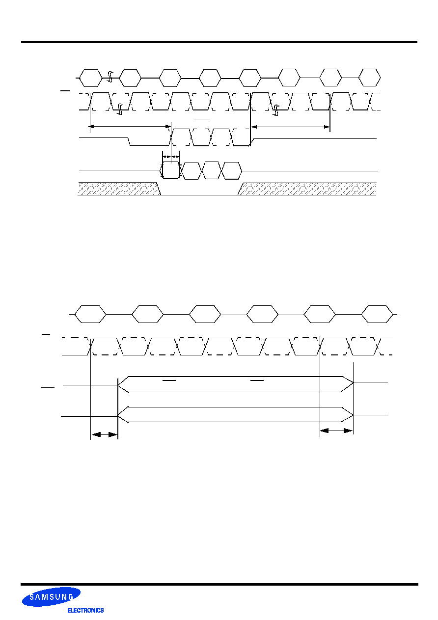
- 28 -
Rev 1.5 Oct. 2005
512M gDDR2 SDRAM
K4N51163QC-ZC
Drive Mode
Drive mode, both Drive(1) and Drive(0), is used for controllers to measure gDDR2 SDRAM Driver impedance. In this mode, all outputs
are driven out tOIT after "enter drive mode" command and all output drivers are turned-off tOIT after "OCD calibration mode exit" com-
mand as the following timing diagram.
NOP
NOP
NOP
NOP
EMRS
DT0
CMD
CK
DQS_in
DQ_in
tDS tDH
WL
OCD adjust mode
OCD calibration mode exit
DT1
DT2
DT3
WR
EMRS
NOP
NOP
CK
DQS
DM
V
IL
(AC)
V
IL
(DC)
V
IH
(AC)
V
IH
(DC)
EMRS
NOP
NOP
NOP
EMRS
CMD
CK
DQS
DQ
Enter Drive mode
OCD calibration mode exit
tOIT
Hi-Z
DQs high for Drive(1)
DQS high & DQS low for Drive(1), DQS low & DQS high for Drive(0)
Hi-Z
DQs low for Drive(0)
tOIT
CK
DQS
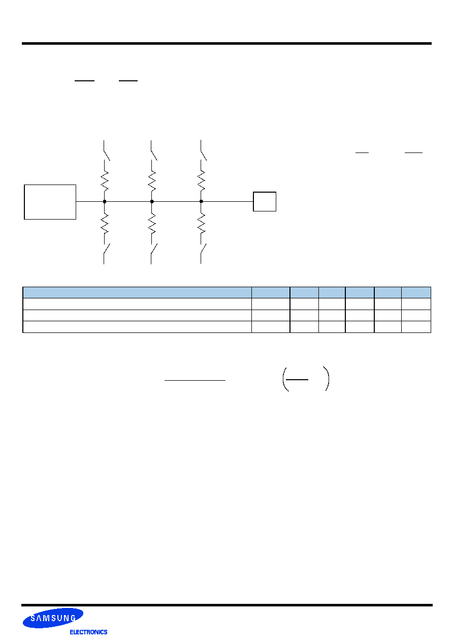
- 29 -
Rev 1.5 Oct. 2005
512M gDDR2 SDRAM
K4N51163QC-ZC
ODT (On Die Termination)
On Die Termination (ODT) is a feature that allows a DRAM to turn on/off termination resistance. For x16 configuration ODT is applied to
each DQ, UDQS/UDQS, LDQS/LDQS, UDM, and LDM signal via the ODT control pin. The ODT feature is designed to improve signal
integrity of the memory channel by allowing the DRAM controller to independently turn on/off termination resistance for any or all DRAM
devices. The ODT function is supported for ACTIVE and STANDBY modes, and turned off and not supported in SELF REFRESH mode.
ODT DC Electrical Characteristics
Note 1: Test condition for Rtt measurements
Measurement Definition for Rtt(eff): Apply V
IH
(AC) and V
IL
(AC) to test pin separately, then measure current I(V
IH
(AC)) and I( V
IL
(AC)) respec-
tively. V
IH
(AC), V
IL
(AC), and VDDQ values defined in SSTL_18
Measurement Definition for VM : Measure voltage (V
M
) at test pin (midpoint) with no load.
Parameter/Condition
Symbol
Min
Nom
Max
Units
Notes
Rtt effective impedance value for EMRS(A6,A2)=0,1; 75 ohm
Rtt1(eff)
60
75
90
ohm
1
Rtt effective impedance value for EMRS(A6,A2)=1,0; 150 ohm
Rtt2(eff)
120
150
180
ohm
1
Rtt mismatch tolerance between any pull-up/pull-down pair
Rtt(mis)
-3.75
+3.75
%
1
Rtt(eff) =
V
IH
(AC)
-
V
IL
(AC)
I(
V
IH
(AC)
) - I(
V
IL
(AC)
)
delta VM =
2 x Vm
V
DDQ
x 100%
- 1
Functional Representation of ODT
Input
Pin
DRAM
VSSQ
VSSQ
VDDQ
VDDQ
Rval2
Rval2
Rval1
Rval1
sw1
sw1
sw2
sw2
Selection among sw1, sw2 and sw3 is determined by "Rtt (nominal)" in EMRS
Termination included on all DQs, DM, DQS, DQS, RDQS, and RDQS pins.
Switch (sw1, sw2, sw3) is enabled by ODT pin.
Input
Buffer
VSSQ
VDDQ
Rval3
Rval3
sw3
sw3
- 30 -
Rev 1.5 Oct. 2005
512M gDDR2 SDRAM
K4N51163QC-ZC
ODT timing for active/standby mode
T0
T1
T2
T3
T4
T5
tAOND
CK
CK
CKE
ODT
Internal
Term Res.
T6
tAOFD
tIS
tIS
tAON,min
tAON,max
tAOF,min
tAOF,max
RTT
V
IH
(AC)
V
IL
(AC)
ODT timing for powerdown mode
T0
T1
T2
T3
T4
T5
CK
CK
CKE
ODT
Internal
Term Res.
T6
tIS
tIS
tAONPD,min
tAOFPD,max
tAONPD,max
tAOFPD,min
RTT
V
IL
(AC)
V
IH
(AC)
- 31 -
Rev 1.5 Oct. 2005
512M gDDR2 SDRAM
K4N51163QC-ZC
ODT timing mode switch at entering power down mode
T-5
T-4
T-3
T-2
T-1
T0
CK
CK
T1
CKE
ODT
Internal
Term Res.
tIS
tAOFD
RTT
tIS
RTT
T2
T3
T4
ODT
Internal
Term Res.
Active & Standby mode
timings to be applied.
Power Down mode tim-
ings to be applied.
tAOFPDmax
tIS
ODT
Internal
Term Res.
tIS
tAOND
RTT
tIS
RTT
ODT
Internal
Term Res.
Active & Standby mode
timings to be applied.
Power Down mode tim-
ings to be applied.
tAONPDmax
tANPD
Entering Slow Exit Active Power Down Mode
or Precharge Power Down Mode.
V
IL
(AC)
V
IL
(AC)
V
IH
(AC)
V
IH
(AC)
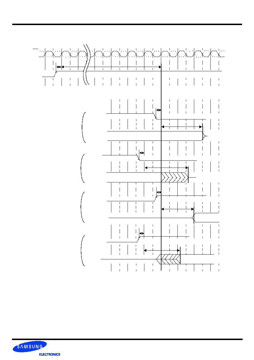
- 32 -
Rev 1.5 Oct. 2005
512M gDDR2 SDRAM
K4N51163QC-ZC
ODT timing mode switch at exiting power down mode
T0
T1
T4
T5
T6
T7
CK
CK
T8
CKE
ODT
Internal
Term Res.
tIS
tAOFPDmax
RTT
tIS
tIS
RTT
T9
T10
T11
ODT
Internal
Term Res.
tAXPD
Active & Standby mode
timings to be applied.
Power Down mode tim-
ings to be applied.
tAOFD
Internal
Term Res.
tIS
RTT
ODT
Active & Standby mode
timings to be applied.
tAOND
Internal
Term Res.
RTT
ODT
tAONPDmax
tIS
Power Down mode tim-
ings to be applied.
V
IH
(AC)
V
IL
(AC)
V
IL
(AC)
V
IH
(AC)
V
IH
(AC)
Exiting from Slow Active Power Down Mode
or Precharge Power Down Mode.
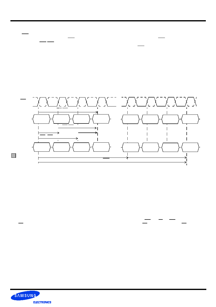
- 33 -
Rev 1.5 Oct. 2005
512M gDDR2 SDRAM
K4N51163QC-ZC
ADDRESS
CK / CK
T0
T2
T1
T3
Tn
Tn+1
Tn+2
Tn+3
COMMAND
Bank A
Row Addr.
Bank A
Activate
Bank A
Col. Addr.
. . . . . . . . . .
. . . . . . . . . .
. . . . . . . . . .
Internal RAS-CAS delay (>= t
RCDmin
)
: "H" or "L"
RAS Cycle time (
>= t
RC
)
additive latency delay (
AL
)
Read A
Post CAS
Bank B
Row Addr.
Bank B
Activate
Bank B
Col. Addr.
Read B
Post CAS
Bank A
Bank A
Precharge
Bank B
Addr.
Bank B
Precharge
Bank A
Row Addr.
Active
Bank A
RAS - RAS delay time (>= t
RRD
)
Read Begins
RCD =1
Addr.
Bank Active (>= t
RAS
)
Bank Precharge time (
>= t
RP
)
CAS-CAS delay time (t
CCD
)
Bank Activate Command Cycle: tRCD = 3, AL = 2, tRP = 3, tRRD = 2, tCCD = 2
Posted CAS operation is supported to make command and data bus efficient for sustainable bandwidths in gDDR2 SDRAM. In this
operation, the gDDR2 SDRAM allows a CAS read or write command to be issued immediately after the RAS bank activate command (or
any time during the RAS-CAS-delay time, tRCD, period). The command is held for the time of the Additive Latency (AL) before it is
issued inside the device. The Read Latency (RL) is controlled by the sum of AL and the CAS latency (CL). Therefore if a user chooses
to issue a R/W command before the tRCDmin, then AL (greater than 0) must be written into the EMR(1). The Write Latency (WL) is
always defined as RL - 1 (read latency -1) where read latency is defined as the sum of additive latency plus CAS latency (RL=AL+CL).
Read or Write operations using AL allow seamless bursts (refer to seamless operation timing diagram examples in Read burst and
Write burst section)
Bank Activate Command
Read and Write Access Modes
After a bank has been activated, a read or write cycle can be executed. This is accomplished by setting RAS high, CS and CAS low at the clock's rising
edge. WE must also be defined at this time to determine whether the access cycle is a read operation (WE high) or a write operation (WE low).
The DDR2 SDRAM provides a fast column access operation. A single Read or Write Command will initiate a serial read or write operation on successive
clock cycles. The boundary of the burst cycle is strictly restricted to specific segments of the page length. For example, the 32Mbit x 4 I/O x 4 Bank chip
has a page length of 2048 bits (defined by CA0-CA9, CA11). The page length of 2048 is divided into 512 or 256 uniquely addressable boundary segments
depending on burst length, 512 for 4 bit burst, 256 for 8 bit burst respectively. A 4-bit or 8 bit burst operation will occur entirely within one of the 512 or 256
groups beginning with the column address supplied to the device during the Read or Write Command (CA0-CA9, CA11). The second, third and fourth
access will also occur within this group segment, however, the burst order is a function of the starting address, and the burst sequence.
A new burst access must not interrupt the previous 4 bit burst operation in case of BL = 4 setting. However, in case of BL = 8 setting, two cases of interrupt
by a new burst access are allowed, one reads interrupted by a read, the other writes interrupted by a write with 4 bit burst boundry respectively. The min-
imum CAS to CAS delay is defined by tCCD, and is a minimum of 2 clocks for read or write cycles.
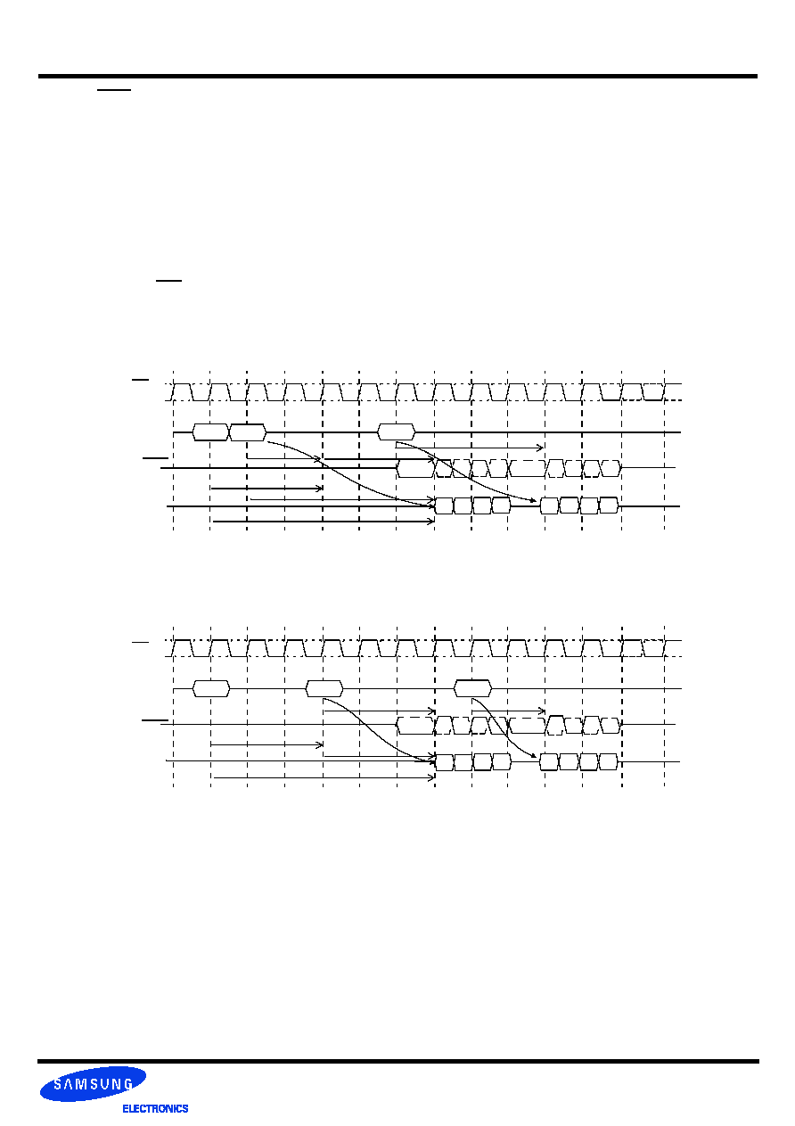
- 34 -
Rev 1.5 Oct. 2005
512M gDDR2 SDRAM
K4N51163QC-ZC
Examples of posted CAS operation
Example 1 Read followed by a write to the same bank
[AL = 2 and CL = 3, RL = (AL + CL) = 5, WL = (RL - 1) = 4]
0
1
2
3
4
5
6
7
8
9
10
11
12
Active
A-Bank
Read
A-Bank
Write
A-Bank
Dout0 Dout1 Dout2 Dout3
Din0Din1Din2Din3
CK/CK
CMD
DQS/DQS
DQ
AL = 2
-1
> = tRCD
CL = 3
> = tRAC
WL = RL -1 = 4
RL = AL + CL = 5
Example 2 Read followed by a write to the same bank
[AL = 0 and CL = 3, RL = (AL + CL) = 3, WL = (RL - 1) = 2]
Active
A-Bank
Read
A-Bank
Write
A-Bank
Dout0 Dout1 Dout2 Dout3
Din0Din1Din2Din3
AL = 0
> = tRCD
CL = 3
> = tRAC
WL = RL -1 = 2
RL = AL + CL = 3
0
1
2
3
4
5
6
7
8
9
10
11
12
-1
CK/CK
CMD
DQS/DQS
DQ
Burst mode operation is used to provide a constant flow of data to memory locations (write cycle), or from memory locations (read
cycle). The parameters that define how the burst mode will operate are burst sequence and burst length. gDDR2 SDRAM supports 4 bit
burst and 8 bit burst modes only. For 8 bit burst mode, full interleave address ordering is supported, however, sequential address order-
ing is nibble based for ease of implementation. The burst type, either sequential or interleaved, is programmable and defined by the
address bit 3 (A3) of the MRS, which is similar to the DDR SDRAM operation. Seamless burst read or write operations are supported.
Unlike DDR devices, interruption of a burst read or write cycle during BL = 4 mode operation is prohibited. However in case of BL = 8
mode, interruption of a burst read or write operation is limited to two cases, reads interrupted by a read, or writes interrupted by a write.
Therefore the Burst Stop command is not supported on gDDR2 SDRAM devices.
Posted CAS
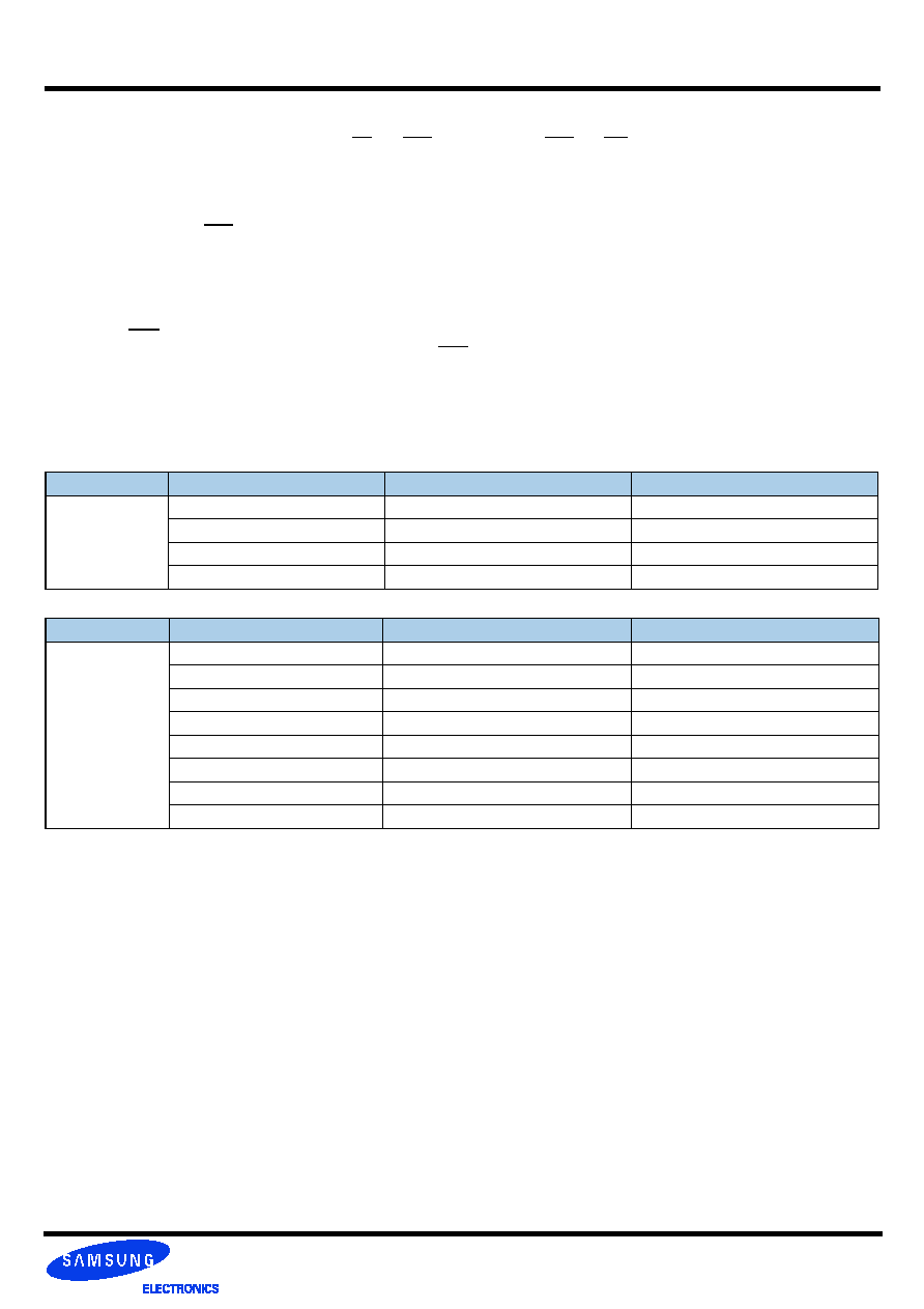
- 35 -
Rev 1.5 Oct. 2005
512M gDDR2 SDRAM
K4N51163QC-ZC
BL = 4
BL = 8
Note : Page length is a function of I/O organization and column addressin
Burst Length
Starting Address (A1 A0)
Sequential Addressing (decimal)
Interleave Addressing (decimal)
4
0 0
0, 1, 2, 3
0, 1, 2, 3
0 1
1, 2, 3, 0
1, 0, 3, 2
1 0
2, 3, 0, 1
2, 3, 0, 1
1 1
3, 0, 1, 2
3, 2, 1, 0
Burst Length
Starting Address (A2 A1 A0)
Sequential Addressing (decimal)
Interleave Addressing (decimal)
8
0 0 0
0, 1, 2, 3, 4, 5, 6, 7
0, 1, 2, 3, 4, 5, 6, 7
0 0 1
1, 2, 3, 0, 5, 6, 7, 4
1, 0, 3, 2, 5, 4, 7, 6
0 1 0
2, 3, 0, 1, 6, 7, 4, 5
2, 3, 0, 1, 6, 7, 4, 5
0 1 1
3, 0, 1, 2, 7, 4, 5, 6
3, 2, 1, 0, 7, 6, 5, 4
1 0 0
4, 5, 6, 7, 0, 1, 2, 3
4, 5, 6, 7, 0, 1, 2, 3
1 0 1
5, 6, 7, 4, 1, 2, 3, 0
5, 4, 7, 6, 1, 0, 3, 2
1 1 0
6, 7, 4, 5, 2, 3, 0, 1
6, 7, 4, 5, 2, 3, 0, 1
1 1 1
7, 4, 5, 6, 3, 0, 1, 2
7, 6, 5, 4, 3, 2, 1, 0
Burst Length and Sequence
The Burst Read command is initiated by having CS and CAS low while holding RAS and WE high at the rising edge of the clock. The
address inputs determine the starting column address for the burst. The delay from the start of the command to when the data from the
first cell appears on the outputs is equal to the value of the read latency (RL). The data strobe output (DQS) is driven low 1 clock cycle
before valid data (DQ) is driven onto the data bus. The first bit of the burst is synchronized with the rising edge of the data strobe (DQS).
Each subsequent data-out appears on the DQ pin in phase with the DQS signal in a source synchronous manner. The RL is equal to an
additive latency (AL) plus CAS latency (CL). The CL is defined by the Mode Register Set (MRS), similar to the existing SDR and DDR
SDRAMs. The AL is defined by the Extended Mode Register Set (1)(EMRS(1)).
gDDR2 SDRAM pin timings are specified for either single ended mode or differen-tial mode depending on the setting of the EMRS
"Enable DQS" mode bit; timing advantages of differential mode are realized in system design. The method by which the gDDR2 SDRAM
pin timings are measured is mode dependent. In single ended mode, timing relationships are measured relative to the rising or falling
edges of DQS crossing at VREF. In differential mode, these timing relationships are measured relative to the crosspoint of DQS and its
complement, DQS. This distinction in timing methods is guaranteed by design and characterization. Note that when differential data
strobe mode is disabled via the EMRS, the complementary pin, DQS, must be tied externally to VSS through a 20 ohm to 10 Kohm
resis-tor to insure proper operation.
Burst Mode Operation
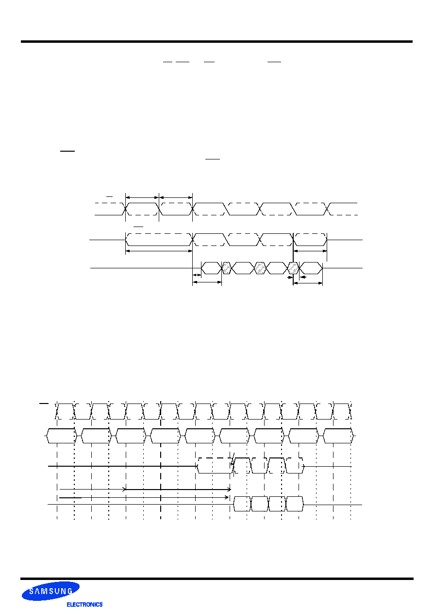
- 36 -
Rev 1.5 Oct. 2005
512M gDDR2 SDRAM
K4N51163QC-ZC
CMD
NOP
NOP
NOP
NOP
NOP
NOP
NOP
DQs
NOP
CK/CK
DOUTA
0
DOUTA
1
DOUTA
2
DOUTA
3
READ A
Posted CAS
AL = 2
CL =3
RL = 5
DQS
=< t
DQSCK
T0
T2
T1
T3
T4
T5
T6
T7
T8
t
CH
t
CL
CK
CK
CK
DQS
DQ
DQS
DQS
t
RPST
Q
t
RPRE
t
DQSQmax
t
QH
t
QH
t
DQSQmax
Q
Q
Q
Burst Read Operation: RL = 5 (AL = 2, CL = 3, BL = 4)
The Burst Write command is initiated by having CS, CAS and WE low while holding RAS high at the rising edge of the clock. The
address inputs determine the starting column address. Write latency (WL) is defined by a read latency (RL) minus one and is equal to
(AL + CL -1). A data strobe signal (DQS) should be driven low (preamble) one clock prior to the WL. The first data bit of the burst cycle
must be applied to the DQ pins at the first rising edge of the DQS following the preamble. The tDQSS specification must be satisfied for
write cycles. The subsequent burst bit data are issued on successive edges of the DQS until the burst length is completed, which is 4 or
8 bit burst. When the burst has finished, any additional data supplied to the DQ pins will be ignored. The DQ Signal is ignored after the
burst write operation is complete. The time from the completion of the burst write to bank precharge is the write recovery time (WR).
gDDR2 SDRAM pin timings are specified for either single ended mode or differen-tial mode depending on the setting of the EMRS
"Enable DQS" mode bit; timing advantages of differential mode are realized in system design. The method by which the gDDR2 SDRAM
pin timings are measured is mode dependent. In single ended mode, timing relationships are measured relative to the rising or falling
edges of DQS crossing at V
REF
. In differential mode, these timing relationships are measured relative to the crosspoint of DQS and its
complement, DQS. This distinction in timing methods is guaranteed by design and characterization. Note that when differential data
strobe mode is disabled via the EMRS, the complementary pin, DQS, must be tied externally to VSS through a 20 ohm to 10K ohm
resistor to insure proper operation.
Burst Read Command

- 37 -
Rev 1.5 Oct. 2005
512M gDDR2 SDRAM
K4N51163QC-ZC
CMD
NOP
NOP
NOP
NOP
NOP
NOP
NOP
DQs
NOP
CK/CK
DOUT A
0
DOUT A
1
DOUT A
2
DOUT A
3
READ A
CAS
CL =3
RL = 3
DQS
=< t
DQSCK
T0
T2
T1
T3
T4
T5
T6
T7
T8
DOUT A
4
DOUT A
5
DOUT A
6
DOUT A
7
CMD
Post CAS
NOP
NOP
NOP
NOP
NOP
DQ's
NOP
CK/CK
T0
Tn-1
T1
Tn
Tn+1
Tn+2
Tn+3
Tn+4
Tn+5
DOUT A
0
DOUT A
1
DOUT A
2
DOUT A
3
DQS
DIN A
0
DIN A
1
DIN A
2
DIN A
3
READ A
WL = RL - 1 = 4
RL =5
Post CAS
WRITE A
t
RTW
(Read to Write turn around time)
NOP
The minimum time from the burst read command to the burst write command is defined by a read-to-write-turn-around-time, which is 4
clocks in case of BL = 4 operation, 6 clocks in case of BL = 8 operation.
Burst Read Operation: RL = 3 (AL = 0 and CL = 3, BL = 8)
Burst Read followed by Burst Write: RL = 5, WL = (RL-1) = 4, BL = 4
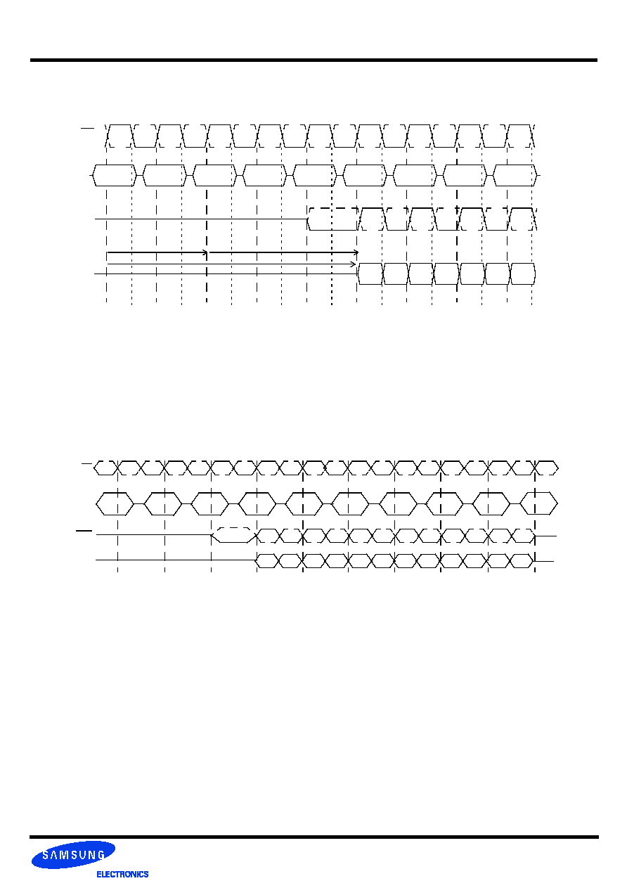
- 38 -
Rev 1.5 Oct. 2005
512M gDDR2 SDRAM
K4N51163QC-ZC
The seamless burst read operation is supported by enabling a read command at every other clock for BL = 4 operation, and every 4
clock for BL = 8 operation. This operation is allowed regardless of same or different banks as long as the banks are activated.
CMD
NOP
NOP
NOP
NOP
NOP
NOP
DQs
NOP
CK/CK
T0
T2
T1
T3
T4
T5
T6
T7
T8
DOUT A
0
DOUT A
1
DOUT A
2
DOUT A
3
READ A0
Post CAS
AL = 2
CL =3
RL = 5
DQS
DOUT A
4
DOUT A
5
DOUT A
6
READ A4
Post CAS
Burst read can only be interrupted by another read with 4 bit burst boundary. Any other case of read interrupt is not allowed.
Read Burst Interrupt Timing Example: (CL=3, AL=0, RL=3, BL=8)
CK/CK
CMD
DQS/DQS
DQs
Read B
Read A
NOP
NOP
NOP
NOP
NOP
NOP
NOP
NOP
A0
A1
A2
A3
B0
B1
B2
B3
B4
B5
B6
B7
Notes:
1. Read burst interrupt function is only allowed on burst of 8. Burst interrupt of 4 is prohibited.
2. Read burst of 8 can only be interrupted by another Read command. Read burst interruption by Write command or Precharge command is prohibited.
3. Read burst interrupt must occur exactly two clocks after previous Read command. Any other Read burst interrupt timings are prohibited.
4. Read burst interruption is allowed to any bank inside DRAM.
5. Read burst with Auto Precharge enabled is not allowed to interrupt.
6. Read burst interruption is allowed by another Read with Auto Precharge command.
7. All command timings are referenced to burst length set in the mode register. They are not referenced to actual burst. For example, Minimum Read to
Precharge timing is AL + BL/2 where BL is the burst length set in the mode register and not the actual burst (which is shorter because of interrupt).
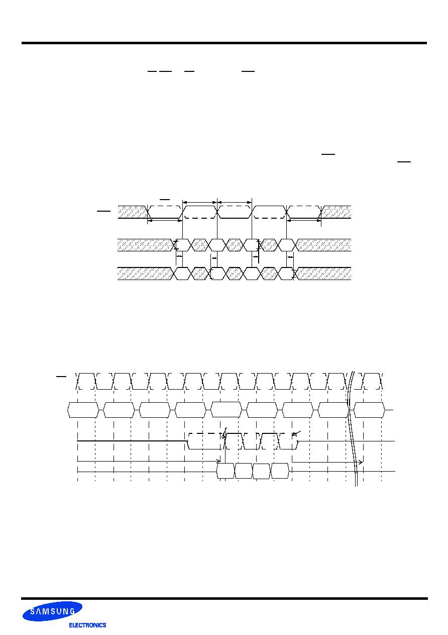
- 39 -
Rev 1.5 Oct. 2005
512M gDDR2 SDRAM
K4N51163QC-ZC
t
DS
t
DS
t
DH
t
WPRE
t
WPST
t
DQSH
t
DQSL
DQS
DQS
D
DMin
DQS/
DQ
DM
t
DH
DMin
DMin
DMin
D
D
D
DQS
V
IL
(ac)
V
IH
(ac)
V
IL
(ac)
V
IH
(ac)
V
IL
(dc)
V
IH
(dc)
V
IL
(dc)
V
IH
(dc)
Burst Write Operation: RL = 5, WL = 4, tWR = 3 (AL=2, CL=3), BL = 4
CMD
DQs
CK/CK
T0
T2
T1
T3
T4
T5
T6
T7
Tn
DQS
NOP
NOP
NOP
NOP
NOP
NOP
NOP
WRITE A
Posted CAS
WL = RL - 1 = 4
< = t
DQSS
> = WR
DIN A
0
DIN A
1
DIN A
2
DIN A
3
Precharge
Completion of
the Burst Write
Burst Write Operation
The Burst Write command is initiated by having CS, CAS and WE low while holding RAS high at the rising edge of the clock. The address inputs determine
the starting column address. Write latency (WL) is defined by a read latency (RL) minus one and is equal to (AL + CL -1);and is the number of clocks of
delay that are required from the time the write command is registered to the clock edge associated to the first DQS strobe. A data strobe signal (DQS)
should be driven low (preamble) one clock prior to the WL. The first data bit of the burst cycle must be applied to the DQ pins at the first rising edge of the
DQS following the preamble. The tDQSS specification must be satisfied for each positive DQS transition to its associated clock edge during write cycles.
The subsequent burst bit data are issued on successive edges of the DQS until the burst length is completed, which is 4 or 8 bit burst. When t he burst
has finished, any additional data supplied to the DQ pins will be ignored. The DQ Signal is ignored after the burst write operation is complete. The time
from the completion of the burst write to bank precharge is the write recovery time (WR).
DDR2 SDRAM pin timings are specified for either single ended mode or differen-tial mode depending on the setting of the EMRS "Enable DQS" mode
bit; timing advantages of differential mode are realized in system design. The method by which the DDR2 SDRAM pin timings are measured is mode de-
pendent. In single ended mode, timing relationships are measured relative to the rising or falling edges of DQS crossing at the specified AC/DC levels. In
differential mode, these timing relationships are measured relative to the crosspoint of DQS and its complement, DQS. This distinction in timing methods
is guaranteed by design and characterization. Note that when differential data strobe mode is disabled via the EMRS, the complementary pin, DQS, must
be tied externally to VSS through a 20 ohm to 10K ohm resistor to insure proper operation.
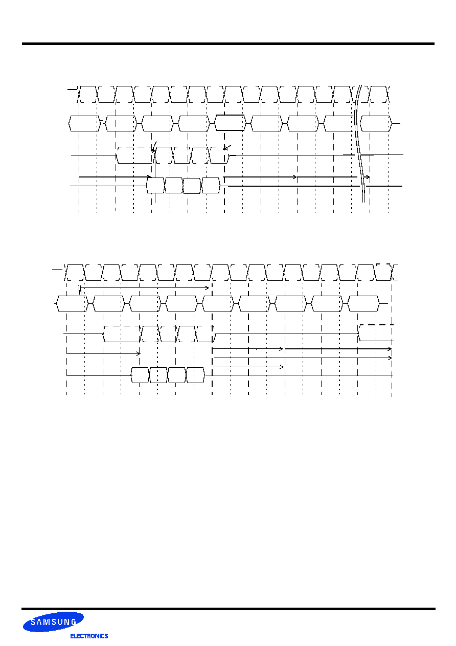
- 40 -
Rev 1.5 Oct. 2005
512M gDDR2 SDRAM
K4N51163QC-ZC
Burst Write Operation: RL = 3, WL = 2, tWR = 2 (AL=0, CL=3), BL = 4
CMD
NOP
NOP
NOP
NOP
Precharge
NOP
DQs
NOP
CK/CK
T0
T2
T1
T3
T4
T5
T6
T7
Tn
WRITE A
CAS
WL = RL - 1 = 2
DQS
< = t
DQSS
> = WR
DIN A
0
DIN A
1
DIN A
2
DIN A
3
Bank A
Completion of
the Burst Write
Activate
> = tRP
Burst Write followed by Burst Read: RL = 5 (AL=2, CL=3), WL = 4, tWTR = 2, BL = 4
CMD
NOP
NOP
NOP
NOP
DQ
CK/CK
T0
T2
T1
T3
T4
T5
T6
T7
T8
DOUT A
0
DOUT A
1
DOUT A
2
DOUT A
3
NOP
DQS
WL = RL - 1 = 4
Post CAS
READ A
NOP
RL =5
AL = 2
CL = 3
NOP
NOP
Write to Read = CL - 1 + BL/2 + tWTR
> = tWTR
T9
The minimum number of clock from the burst write command to the burst read command is [CL - 1 + BL/2 + tWTR]. This tWTR is not a
write recovery time (tWR) but the time required to transfer the 4bit write data from the input buffer into sense amplifiers in the array.
tWTR is defined in AC spec table of this data sheet.
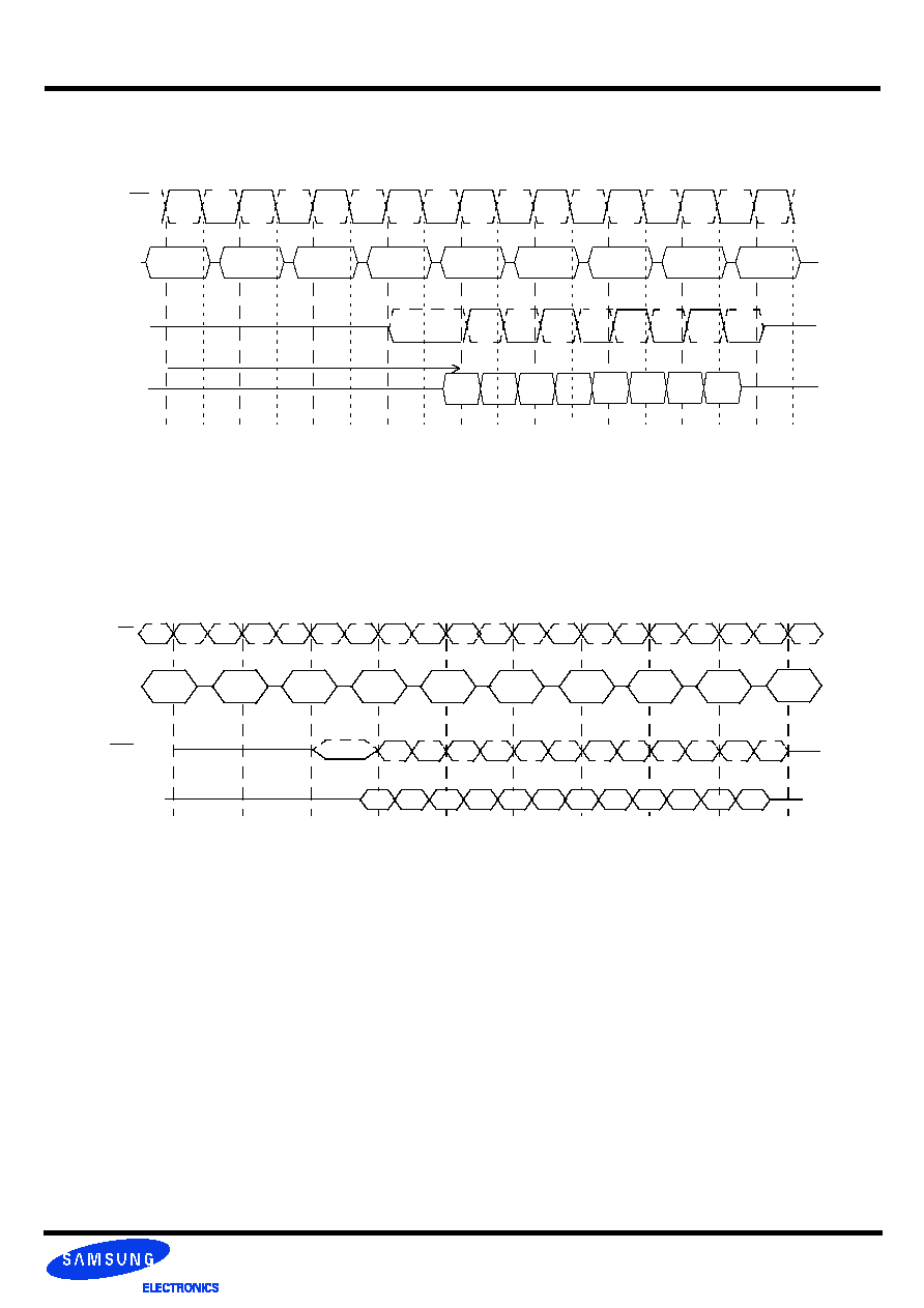
- 41 -
Rev 1.5 Oct. 2005
512M gDDR2 SDRAM
K4N51163QC-ZC
Seamless Burst Write Operation: RL = 5, WL = 4, BL=4
The seamless burst write operation is supported by enabling a write command every other clock for BL = 4 operation, every four clocks
for BL = 8 operation. This operation is allowed regardless of same or different banks as long as the banks are activated.
CMD
NOP
NOP
NOP
NOP
NOP
NOP
DQ's
NOP
CK/CK
T0
T2
T1
T3
T4
T5
T6
T7
T8
DIN A
0
DIN A
1
DIN A
2
DIN A
3
WRITE A0
Post CAS
WL = RL - 1 = 4
DQS
WRITE A1
Post CAS
DIN A
0
DIN A
1
DIN A
2
DIN A
3
Notes:
1. Write burst interrupt function is only allowed on burst of 8. Burst interrupt of 4 is prohibited.
2. Write burst of 8 can only be interrupted by another Write command. Write burst interruption by Read command or Precharge command is prohibited.
3. Write burst interrupt must occur exactly two clocks after previous Write command. Any other Write burst interrupt timings are prohibited.
4. Write burst interruption is allowed to any bank inside DRAM.
5. Write burst with Auto Precharge enabled is not allowed to interrupt.
6. Write burst interruption is allowed by another Write with Auto Precharge command.
7. All command timings are referenced to burst length set in the mode register. They are not referenced to actual burst. For example, minimum Write to
Precharge timing is WL+BL/2+tWR where tWR starts with the rising clock after the un-interrupted burst end and not from the end of actual burst end.
Writes intrrupted by a write
Burst write can only be interrupted by another write with 4 bit burst boundary. Any other case of write interrupt is not allowed.
Write Burst Interrupt Timing Example: (CL=3, AL=0, RL=3, WL=2, BL=8)
CK/CK
CMD
DQS/DQS
DQs
NOP
NOP
NOP
NOP
NOP
NOP
NOP
NOP
A0
A1
A2
A3
B0
B1
B2
B3
B5
B6
B7
Write B
Write A
B4
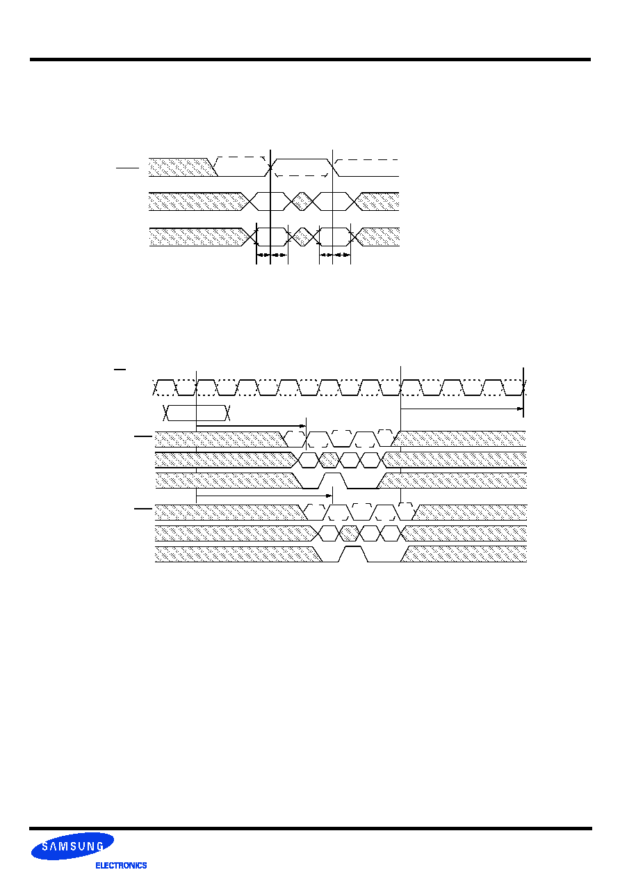
- 42 -
Rev 1.5 Oct. 2005
512M gDDR2 SDRAM
K4N51163QC-ZC
One write data mask (DM) pin for each 8 data bits (DQ) will be supported on gDDR2 SDRAMs, Consistent with the implementation on
gDDR SDRAMs. It has identical timings on write operations as the data bits, and though used in a uni-directional manner, is internally
loaded identically to data bits to insure matched system timing. DM of x16 bit organization is not used during read cycles.
DQS/
DQ
DM
t
DS
t
DH
t
DS
t
DH
Write
CK
CK
COMMAND
DQS/DQS
DQ
DM
Case 2 : max t
DQSS
DQS/DQS
DQ
DM
t
DQSS
t
DQSS
t
WR
Case 1 : min t
DQSS
DQS
V
IL
(ac)
V
IH
(ac)
V
IL
(dc)
V
IH
(dc)
V
IL
(ac)
V
IL
(dc)
V
IH
(ac)
V
IH
(dc)
Write data mask
Data Mask Timing
Data Mask Function, WL=3, AL=0, BL = 4 shown
- 43 -
Rev 1.5 Oct. 2005
512M gDDR2 SDRAM
K4N51163QC-ZC
The Precharge Command is used to precharge or close a bank that has been activated. The Precharge Command is triggered when
CS, RAS and WE are low and CAS is high at the rising edge of the clock. The Precharge Command can be used to precharge each
bank independently or all banks simultaneously. Three address bits A10, BA0 and BA1 for 256Mb are used to define which bank to pre-
charge when the command is issued.
Minimum Read to precharge command spacing to the same bank = AL + BL/2 clocks.
For the earliest possible precharge, the precharge command may be issued on the rising edge which is "Additive latency(AL) + BL/2
clocks" after a Read command. A new bank active (command) may be issued to the same bank after the RAS precharge time (t
RP
). A
precharge command cannot be issued until t
RAS
is satisfied.
The minimum Read to Precharge spacing has also to satisfy a minimum analog time from the rising clock edge that initiates the last 4-
bit prefetch of a Read to Precharge command. This time is called tRTP (Read to Precharge). For BL = 4 this is the time from the actual
read (AL after the Read command) to Precharge command. For BL = 8 this is the time from AL + 2 clocks after the Read to the Pre-
charge command.
A10
BA1
BA0
Precharged
Bank(s)
Remarks
LOW
LOW
LOW
Bank 0 only
LOW
LOW
HIGH
Bank 1 only
LOW
HIGH
LOW
Bank 2 only
LOW
HIGH
HIGH
Bank 3 only
HIGH
DON'T CARE
DON'T CARE
All Banks
Bank Selection for Precharge by Address Bits
Burst Read Operation Followed by Precharge
Example 1: Burst Read Operation Followed by Precharge:
RL = 4, AL = 1, CL = 3, BL = 4, t
RTP
<= 2 clocks
CMD
NOP
NOP
Precharge
NOP
DQ's
NOP
CK/CK
DOUT A
0
DOUT A
1
DOUT A
2
DOUT A
3
READ A
Post CAS
RL =4
DQS
Active
Bank A
> = t
RP
NOP
CL =3
NOP
> = t
RAS
T0
T2
T1
T3
T4
T5
T6
T7
T 8
AL + BL/2 clks
AL = 1
CL = 3
> = t
RTP
Precharge Command
- 44 -
Rev 1.5 Oct. 2005
512M gDDR2 SDRAM
K4N51163QC-ZC
Example 2: Burst Read Operation Followed by Precharge:
RL = 4, AL = 1, CL = 3, BL = 8, t
RTP
<= 2 clocks
CMD
NOP
NOP
NOP
NOP
DQ's
NOP
CK/CK
DOUT A
0
DOUT A
1
DOUT A
2
DOUT A
3
READ A
Post CAS
RL =4
DQS
Precharge A
NOP
T0
T2
T1
T3
T4
T5
T6
T7
T 8
AL + BL/2 clks
AL = 1
CL = 3
> = t
RTP
DOUT A
4
DOUT A
5
DOUT A
6
DOUT A
8
first 4-bit prefetch
second 4-bit prefetch
NOP
Example 3: Burst Read Operation Followed by Precharge :
RL = 5, AL = 2, CL = 3, BL = 4, t
RTP
<= 2 clocks
DQ's
CK/CK
DOUT A
0
DOUT A
1
DOUT A
2
DOUT A
3
AL = 2
CL =3
RL =5
DQS
> = t
RP
CL =3
> = t
RAS
T0
T2
T1
T3
T4
T5
T6
T7
T 8
AL + BL/2 clks
> = t
RTP
CMD
NOP
NOP
NOP
NOP
Precharge A
READ A
Posted CAS
Activate
Bank A
NOP
NOP
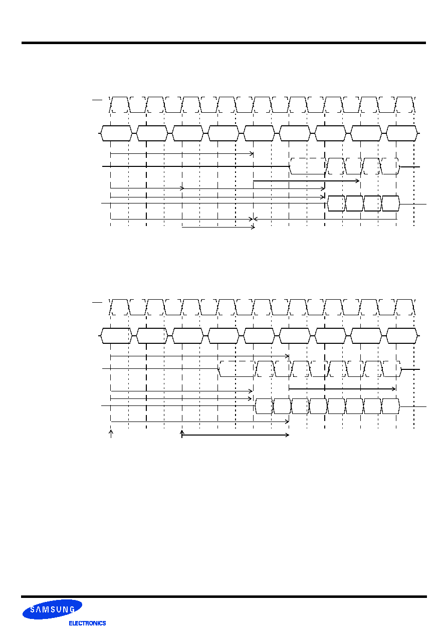
- 45 -
Rev 1.5 Oct. 2005
512M gDDR2 SDRAM
K4N51163QC-ZC
Example 4: Burst Read Operation Followed by Precharge :
RL = 6, AL = 2, CL = 4, BL = 4, t
RTP
<= 2 clocks
CMD
DQ's
CK/CK
DOUT A
0
DOUT A
1
DOUT A
2
DOUT A
3
AL = 2
CL =4
RL = 6
DQS
> = t
RP
CL =4
> = t
RAS
T0
T2
T1
T3
T4
T5
T6
T7
T 8
AL + BL/2 Clks
> = t
RTP
Example 5: Burst Read Operation Followed by Precharge :
RL = 4, AL = 0, CL = 4, BL = 8, t
RTP
> 2 clocks
CMD
NOP
DQ's
CK/CK
DOUT A
0
DOUT A
1
DOUT A
2
DOUT A
3
READ A
Post CAS
AL = 0
CL =4
RL = 4
DQS
> = t
RP
> = t
RAS
T0
T2
T1
T3
T4
T5
T6
T7
T 8
AL + 2 Clks + max{tRTP;2 tCK}*
* : rounded to next integer
DOUT A
4
DOUT A
5
DOUT A
6
DOUT A
8
first 4-bit prefetch
second 4-bit prefetch
> = t
RTP
NOP
NOP
NOP
NOP
Precharge A
READ A
Post CAS
Activate
Bank A
NOP
NOP
NOP
NOP
NOP
Precharge A
Activate
Bank A
NOP
NOP

- 46 -
Rev 1.5 Oct. 2005
512M gDDR2 SDRAM
K4N51163QC-ZC
Minimum Write to Precharge Command spacing to the same bank = WL + BL/2 clks + tWR For write cycles, a delay must be satisfied
from the completion of the last burst write cycle until the Precharge Command can be issued. This delay is known as a write recovery
time (tWR) referenced from the completion of the burst write to the precharge command. No Precharge command should be issued
prior to the tWR delay.
Example 1 : Burst Write followed by Precharge: WL = (RL-1) =3, BL=4
Example 2 : Burst Write followed by Precharge: WL = (RL-1) = 4, BL=4
CMD
DQs
CK/CK
T0
T2
T1
T3
T4
T5
T6
T7
T 8
WL = 3
DQS
> = t
WR
CMD
NOP
NOP
NOP
NOP
NOP
NOP
DQs
NOP
CK/CK
T0
T2
T1
T3
T4
T5
T6
T7
T 9
DIN A
0
DIN A
1
DIN A
2
DIN A
3
WRITE A
Posted CAS
WL = 4
DQS
> = t
WR
Precharge A
Completion of the Burst Write
NOP
NOP
NOP
NOP
NOP
NOP
NOP
WRITE A
Posted CAS
Precharge A
Completion of the Burst Write
DIN A
0
DIN A
1
DIN A
2
DIN A
3
Burst Write followed by Precharge

- 47 -
Rev 1.5 Oct. 2005
512M gDDR2 SDRAM
K4N51163QC-ZC
If A10 is high when a Read Command is issued, the Read with Auto-Precharge function is engaged. The gDDR2 SDRAM starts an
auto Precharge operation on the rising edge which is (AL + BL/2) cycles later than the read with AP command if tRAS(min) and tRTP are
satisfied.
If tRAS(min) is not satisfied at the edge, the start point of auto-precharge operation will be delayed until tRAS(min) is satisfied.
If tRTP(min) is not satisfied at the edge, the start point of auto-precharge operation will be delayed until tRTP(min) is satisfied.
In case the internal precharge is pushed out by tRTP, tRP starts at the point where the internal precharge happens (not at the next rising
clock edge after this event). So for BL = 4 the minimum time from Read_AP to the next Activate command becomes AL + (tRTP + tRP)*
(see example 2) for BL = 8 the time from Read_AP to the next Activate is AL + 2 + (tRTP + tRP)*, where "*" means: "rouded up to the
next integer". In any event internal precharge does not start earlier than two clocks after the last 4-bit prefetch.
A new bank activate (command) may be issued to the same bank if the following two conditions are satisfied simultaneously.
(1) The RAS precharge time (tRP) has been satisfied from the clock at which the auto precharge begins.
(2) The RAS cycle time (tRC) from the previous bank activation has been satisfied.
Before a new row in an active bank can be opened, the active bank must be precharged using either the Precharge Command or the
auto-precharge function. When a Read or a Write Command is given to the gDDR2 SDRAM, the CAS timing accepts one extra address,
column address A10, to allow the active bank to automatically begin precharge at the earliest possible moment during the burst read or
write cycle. If A10 is low when the READ or WRITE Command is issued, then normal Read or Write burst operation is executed and the
bank remains active at the completion of the burst sequence. If A10 is high when the Read or Write Command is issued, then the auto-
precharge function is engaged. During auto-precharge, a Read Command will execute as normal with the exception that the active bank
will begin to precharge on the rising edge which is CAS latency (CL) clock cycles before the end of the read burst.
Auto-precharge also be implemented during Write commands. The precharge operation engaged by the Auto precharge command will
not begin until the last data of the burst write sequence is properly stored in the memory array.
This feature allows the precharge operation to be partially or completely hidden during burst read cycles (dependent upon CAS latency)
thus improving system performance for random data access. The RAS lockout circuit internally delays the Precharge operation until the
array restore operation has been completed (tRAS satisfied) so that the auto precharge command may be issued with any read or write
command.
Burst Read with Auto Precharge
Auto-Precharge Operation
- 48 -
Rev 1.5 Oct. 2005
512M gDDR2 SDRAM
K4N51163QC-ZC
Example 1: Burst Read Operation with Auto Precharge:
RL = 4, AL = 1, CL = 3, BL = 8, t
RTP
<= 2 clocks
CMD
NOP
NOP
NOP
NOP
DQ's
NOP
CK/CK
DOUT A
0
DOUT A
1
DOUT A
2
DOUT A
3
READ A
Post CAS
RL =4
DQS
T0
T2
T1
T3
T4
T5
T6
T7
T 8
AL + BL/2 clks
AL = 1
CL = 3
> = t
RTP
DOUT A
4
DOUT A
5
DOUT A
6
DOUT A
8
first 4-bit prefetch
second 4-bit prefetch
NOP
t
RTP
NOP
Precharge begins here
Activate
Bank A
> = t
RP
Autoprecharge
Example 2: Burst Read Operation with Auto Precharge:
RL = 4, AL = 1, CL = 3, BL = 4, t
RTP
> 2 clocks
CK/CK
T0
T2
T1
T3
T4
T5
T6
T7
T 8
CMD
NOP
NOP
NOP
NOP
DQ's
NOP
DOUT A
0
DOUT A
1
DOUT A
2
DOUT A
3
READ A
Post CAS
RL =4
DQS
> = AL + tRTP + tRP
AL = 1
CL = 3
4-bit prefetch
NOP
t
RTP
NOP
Precharge begins here
Activate
Bank A
Autoprecharge
t
RP
- 49 -
Rev 1.5 Oct. 2005
512M gDDR2 SDRAM
K4N51163QC-ZC
Example 3: Burst Read with Auto Precharge Followed by an activation to the Same Bank
(tRC Limit):
RL = 5 (AL = 2, CL = 3, internal tRCD = 3, BL = 4, t
RTP
<= 2 clocks)
CMD
NOP
NOP
NOP
NOP
NOP
DQ's
NOP
CK/CK
T0
T2
T1
T3
T4
T5
T6
T7
T8
DOUT A
0
DOUT A
1
DOUT A
2
DOUT A
3
READ A
Post CAS
AL = 2
CL =3
RL = 5
DQS
Activate
Bank A
> = t
RP
A10 = 1
Auto Precharge Begins
CL =3
> = t
RC
NOP
> = tRas(min)
Example 4: Burst Read with Auto Precharge Followed by an Activation to the Same Bank
(tRP Limit):
RL = 5 (AL = 2, CL = 3, internal tRCD = 3, BL = 4, t
RTP
<= 2 clocks)
CMD
NOP
NOP
NOP
NOP
NOP
DQ's
NOP
CK/CK
T0
T2
T1
T3
T4
T5
T6
T7
T8
DOUT A
0
DOUT A
1
DOUT A
2
DOUT A
3
READ A
Post CAS
AL = 2
CL =3
RL = 5
DQS
Activate
Bank A
> = t
RP
A10 = 1
Auto Precharge Begins
CL =3
> = t
RC
NOP
> = tRas(min)
- 50 -
Rev 1.5 Oct. 2005
512M gDDR2 SDRAM
K4N51163QC-ZC
If A10 is high when a Write Command is issued, the Write with Auto-Precharge function is engaged. The gDDR2 SDRAM automatically
begins precharge operation after the completion of the burst write plus write recovery time (tWR). The bank undergoing auto-precharge
from the completion of the write burst may be reactivated if the following two conditions are satisfied.
(1) The data-in to bank activate delay time (WR + tRP) has been satisfied.
(2) The RAS cycle time (tRC) from the previous bank activation has been satisfied.
CMD
NOP
NOP
NOP
NOP
NOP
Bank A
DQs
NOP
CK/CK
T0
T2
T1
T3
T4
T5
T6
T7
Tm
DIN A
0
DIN A
1
DIN A
2
DIN A
3
WRA BankA
Post CAS
WL =RL - 1 = 2
DQS/DQS
A10 = 1
Auto Precharge Begins
NOP
> =
WR
Completion of the Burst Write
Active
> = t
RP
> = t
RC
Burst Write with Auto-Precharge (tWR + tRP): WL = 4, tWR =2, tRP=3, BL=4
CMD
NOP
NOP
NOP
NOP
NOP
Bank A
DQs
NOP
CK/CK
T0
T4
T3
T5
T6
T7
T8
T9
T12
DIN A
0
DIN A
1
DIN A
2
DIN A
3
WRA Bank A
Post CAS
WL =RL - 1 = 4
DQS/DQS
A10 = 1
Auto Precharge Begins
NOP
> =
WR
Completion of the Burst Write
Active
> = t
RP
> = t
RC
Burst Write with Auto-Precharge (tRC Limit): WL = 2, tWR =2, tRP=3, BL=4
Burst Write with Auto-Precharge
- 51 -
Rev 1.5 Oct. 2005
512M gDDR2 SDRAM
K4N51163QC-ZC
Note :
1. The value of tRTP is decided by the equation : max( RU<tRTP/tCK>, 2) where RU stands for round up. This is required to cover the max tCK case,
which is 8 ns.
2. For a given bank, the precharge period of tRP should be counted from the latest precharge command issued to that bank. Similarly, the precharge
period of tRPall should be counted from the latest precharge all command ossued to the DRAM.
From Command
To Command
Minimum Delay beween"From Com-
mand" to "To Command"
Unit
Note
Read w/AP
Precharge ( to same Bank as Read w/AP)
AL + BL/2 + tRTP - 2 * tCK
clks
1, 2
Precharge All
AL + BL/2 + tRTP - 2 * tCK
clks
1, 2
Write w/AP
Precharge ( to same Bank as Write w/AP)
WL + BL/2 + WR
clks
2
Precharge All
WL + BL/2 + WR
clks
2
Precharge
Precharge ( to same Bank as Precharge)
1 * tCK
clks
2
Precharge All
1 * tCK
clks
2
Precharge All
Precharge
1 * tCK
clks
2
Precharge All
1 * tCK
clks
2
Refresh Command
When CS, RAS and CAS are held low and WE high at the rising edge of the clock, the chip enters the Refresh mode (REF). All banks
of the gDDR2 SDRAM must be precharged and idle for a minimum of the Precharge time (tRP) before the Refresh command (REF) can
be applied. An address counter, internal to the device, supplies the bank address during the refresh cycle. No control of the external
address bus is required once this cycle has started.
When the refresh cycle has completed, all banks of the gDDR2 SDRAM will be in the precharged (idle) state. A delay between the
Refresh command (REF) and the next Activate command or subsequent Refresh command must be greater than or equal to the
Refresh cycle time (tRFC).
To allow for improved efficiency in scheduling and switching between tasks, some flexibility in the absolute refresh interval is provided.
A maximum of eight Refresh commands can be posted to any given gDDR2 SDRAM, meaning that the maximum absolute interval
between any Refresh command and the next Refresh command is 9 * tREFI.
CMD
CK/CK
T0
T2
T1
T3
Tm
Tn
Tn + 1
CKE
> = t
RP
> = t
RFC
> = t
RFC
High
NOP
REF
REF
NOP
ANY
Precharge
NOP
Precharge & Auto Precharge Clarification
- 52 -
Rev 1.5 Oct. 2005
512M gDDR2 SDRAM
K4N51163QC-ZC
The gDDR2 SDRAM device has a built-in timer to accommodate Self Refresh operation. The Self Refresh Command is defined by hav-
ing CS, RAS, CAS and CKE held low with WE high at the rising edge of the clock. ODT must be turned off before issuing Self Refresh
command, by either driving ODT pin low or using EMRS command. Once the Command is registered, CKE must be held low to keep the
device in Self Refresh mode. When the gDDR2 SDRAM has entered Self Refresh mode all of the external signals except CKE, are
"don't care". Since CKE is an SSTL 2 input, V
REF
must be maintained during Self Refresh operation. The DRAM initiates a minimum of
one one Auto Refresh command internally within tCKE period once it enters Self Refresh mode. The clock is internally disabled during
Self Refresh Operation to save power. The minimum time that the gDDR2 SDRAM must remain in Self Refresh mode is tCKE. The user
may change the external clock frequency or halt the external clock one clock after Self-Refresh entry is registered, however, the clock
must be restarted and stable before the device can exit Self Refresh operation. Once Self Refresh Exit command is registered, a delay
equal or longer than the tXSNR or tXSRD must be satisfied before a valid command can be issued to the device. CKE must remain high
for the entire Self Refresh exit period tXSRD for proper operation. Upon exit from Self Refresh, the gDDR2 SDRAM can be put back into
Self Refresh mode after tXSRD expires. NOP or deselect commands must be registered on each positive clock edge during the Self
Refresh exit interval. ODT should also be turned off during tXSRD. Upon exit from Self Refresh, the gDDR2 SDRAM requires a mini-
mum of one extra auto refresh command before it is put back into Self Refresh mode.
- Device must be in the "All banks idle" state prior to entering Self Refresh mode.
- ODT must be turned off tAOFD before entering Self Refresh mode, and can be turned on again when tXSRD timing is satisfied.
- tXSRD is applied for a Read or a Read with autoprecharge command.
- tXSNR is applied for any command except a Read or a Read with autoprecharge command.
CMD
CK
T0
T2
T1
Tm
Tn
CKE
T3
T4
T5
ODT
Self
Refresh
T6
NOP
tAOFD
CK
> = tXSNR
> = tXSRD
tRP*
Valid
tCK
tCH tCL
tIS
tIS
tIS
tIS tIH
NOP
NOP
V
IL
(AC)
V
IL
(AC)
V
IH
(AC)
V
IL
(DC)
V
IH
(AC)
V
IL
(AC)
V
IH
(DC)
Self Refresh Operation
- 53 -
Rev 1.5 Oct. 2005
512M gDDR2 SDRAM
K4N51163QC-ZC
Power-down is synchronously entered when CKE is registered low (along with Nop or Deselect command). CKE is not allowed to go
low while mode register or extended mode register command time, or read or write operation is in progress. CKE is allowed to go low
while any of other operations such as row activation, precharge or autoprecharge, or auto-refresh is in progress, but power-down IDD
spec will not be applied until finishing those operations. Timing diagrams are shown in the following pages with details for entry into
power down.
The DLL should be in a locked state when power-down is entered. Otherwise DLL should be reset after exiting power-down mode for
proper read operation. DRAM design guarantees it's DLL in a locked state with any CKE intensive operations as long as DRAM control-
ler complies with DRAM specifications. Following figures show two examples of CKE intensive applications. In both examples, DRAM
maintains DLL in a locked state throughout the period.
Power-Down
tCKE
CK
CK
CKE
DRAM guarantees all AC and DC timing & voltage specifications and proper DLL operation with intensive CKE operation
<Example of CKE instensive environment 1>
tXP
tXP
CK
CK
CKE
guarantees all AC and DC timing & voltage specifications and DLL operation with temperature and voltage drift.
<Example of CKE Iintensive enviroment 2>
REF
REF
tREFI = 7.8 us
The pattern shown above can repeat over a long period of time. With this pattern, DRAM guarantees all DRAM
CMD
tCKE
tCKE
tCKE
tCKE

- 54 -
Rev 1.5 Oct. 2005
512M gDDR2 SDRAM
K4N51163QC-ZC
If power-down occurs when all banks are idle, this mode is referred to as precharge power-down; if power-down occurs
when there is a row active in any bank, this mode is referred to as active power-down. Entering power-down deactivates
the input and output buffers, excluding CK, CK, ODT and CKE. Also the DLL is disabled upon entering precharge power-
down or slow exit active power-down, but the DLL is kept enabled during fast exit active power-down. In power-down
mode, CKE low and a stable clock signal must be maintained at the inputs of the gDDR2 SDRAM, and ODT should be in
a valid state but all other input signals are "Don't Care". CKE low must be maintained until tCKE has been satisfied.
Power-down duration is limited by 9 times tREFI of the device.
The power-down state is synchronously exited when CKE is registered high (along with a Nop or Deselect command).
CKE high must be maintained until tCKE has been satisfied. A valid, executable command can be applied with power-
down exit latency, tXP, tXARD, or tXARDS, after CKE goes high. Power-down exit latency is defined at AC spec table of
this data sheet.
t
IS
t
IS
CK/CK
CKE
Command
VALID
NOP
VALID
Don't Care
NOP
t
XP,
t
XARD,
Enter Power-Down mode
t
CKE
t
IH
t
IH
t
CKE
t
XARDS
VALID
t
IH
Exit Power-Down mode
t
IS
t
IH
t
CKE
t
IH
VALID
t
IS
V
IH
(AC)
V
IH
(DC)
V
IL
(DC)
V
IH
(AC)
V
IH
(DC)
V
IL
(AC)
V
IH
(DC)
V
IH
(AC)
Basic Power Down Entry and Exit timing diagram

- 55 -
Rev 1.5 Oct. 2005
512M gDDR2 SDRAM
K4N51163QC-ZC
CK
CMD
CKE
DQ
DQS
CMD
CKE
DQ
DQS
CMD
CKE
DQ
DQS
CMD
CKE
DQ
DQS
RDA
RDA
BL=8
PRE
PRE
AL + BL/2
with tRTP = 7.5ns
& tRAS min satisfied
AL + BL/2
with tRTP = 7.5ns
& tRAS min satisfied
Read with Autoprecharge to power down entry
CK
CK
CK
Start internal precharge
AL + CL
AL + CL
CKE should be kept high until the end of burst operation.
AL + CL
BL=4
CKE should be kept high
CKE should be kept high
until the end of burst operation.
AL + CL
T0
Tx
Tx+2
Tx+3
Tx+4
Tx+5
Tx+6
T1
T2
Tx+1
Tx+7
Tx+8
Tx+9
Q
Q
Q
Q
Q
Q
Q
Q
Q
Q
Q
Q
CKE should be kept high until the end of burst operation.
until the end of burst operation.
Q
Q
Q
Q
Q
Q
Q
Q
RD
BL=4
RD
BL=8
Read operation starts with a read command and
Q
Q
Q
Q
T0
Tx
Tx+2
Tx+3
Tx+4
Tx+5
Tx+6
T1
T2
Tx+1
Tx+7
Tx+8
Tx+9
T0
Tx
Tx+2
Tx+3
Tx+4
Tx+5
Tx+6
T1
T2
Tx+1
Tx+7
Tx+8
Tx+9
T0
Tx
Tx+2
Tx+3
Tx+4
Tx+5
Tx+6
T1
T2
Tx+1
Tx+7
Tx+8
Tx+9
DQS
DQS
DQS
DQS
Read to power down entry
- 56 -
Rev 1.5 Oct. 2005
512M gDDR2 SDRAM
K4N51163QC-ZC
CMD
CKE
DQ
DQS
CMD
CKE
DQ
DQS
T0
Tm+1
Tm+3
Tx
Tx+1
Tx+2
Ty
T1
Tm
Tm+2
Ty+1
Ty+2
Ty+3
WR
WR
BL=8
CMD
CKE
DQ
DQS
CMD
CKE
DQ
DQS
T0
Tm+1
Tm+3
Tx
Tx+1
Tx+2
Tx+3
T1
Tm
Tm+2
Tx+4
Tx+5
Tx+6
WRA
WRA
BL=8
PRE
PRE
D
D
D
D
D
D
D
D
D
D
D
D
tWTR
tWTR
WR*1
D
D
D
D
D
D
D
D
D
D
D
D
WR
*1
Write with Autoprecharge to power down entry
CK
CK
CK
CK
WL
BL=4
BL=4
WL
WL
WL
T0
Tm+1
Tm+3
Tm+4
Tm+5
Tx
Tx+1
T1
Tm
Tm+2
Tx+2
Tx+3
Tx+4
CK
CK
* 1: WR is programmed through MRS
T0
Tm+1
Tm+3
Tm+4
Tm+5
Tx
Tx+1
T1
Tm
Tm+2
Tx+2
Tx+3
Tx+4
DQS
DQS
DQS
DQS
Write to power down entry
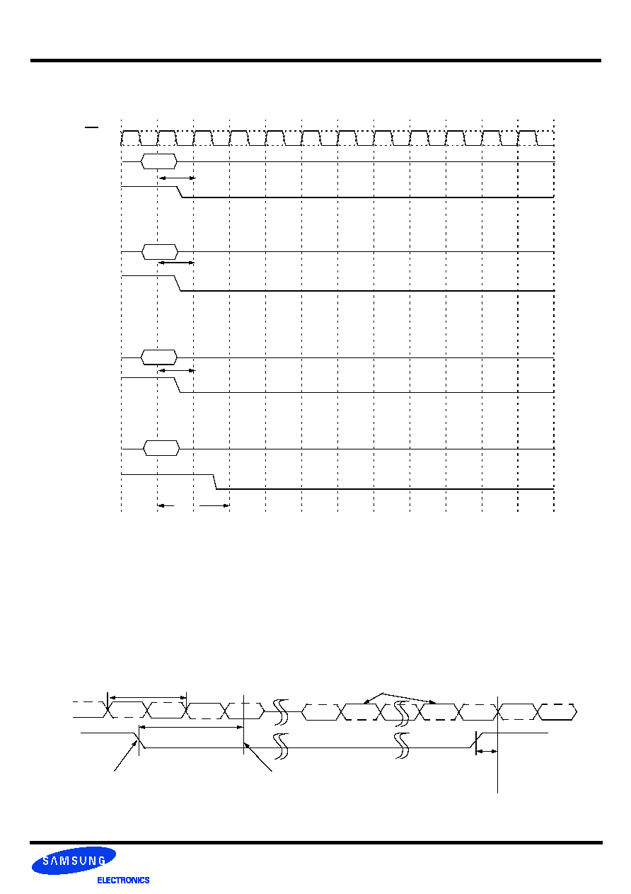
- 57 -
Rev 1.5 Oct. 2005
512M gDDR2 SDRAM
K4N51163QC-ZC
CMD
CKE
CMD
CKE
T0
T3
T5
T6
T7
T8
T9
T1
T2
T4
T10
CMD
CKE
CMD
CKE
CKE can go to low one clock after an Active command
PR or
MRS or
PRA
EMRS
REF
ACT
tMRD
Active command to power down entry
Precharge/Precharge all command to power down entry
MRS/EMRS command to power down entry
CK
CK
CKE can go to low one clock after a Precharge or Precharge all command
CKE can go to low one clock after an Auto-refresh command
T11
DRAM requires CKE to be maintained "HIGH" for all valid operations as defined in this data sheet. If CKE asynchronously drops "LOW"
during any valid operation DRAM is not guaranteed to preserve the contents of array. If this event occurs, memory controller must sat-
isfy DRAM timing specification tDelay before turning off the clocks. Stable clocks must exist at the input of DRAM before CKE is raised
"HIGH" again. DRAM must be fully re-initialized (steps 4 thru 13) as described in initialization sequence. DRAM is ready for normal oper-
ation after the initialization sequence. See AC timing parametric table for tDelay specification.
Asynchronous CKE Low Event
Refresh command to power down entry
tCK
CK
CK#
tDelay
CKE
CKE asynchronously drops low
Clocks can be turned
off after this point
Stable clocks
tIS
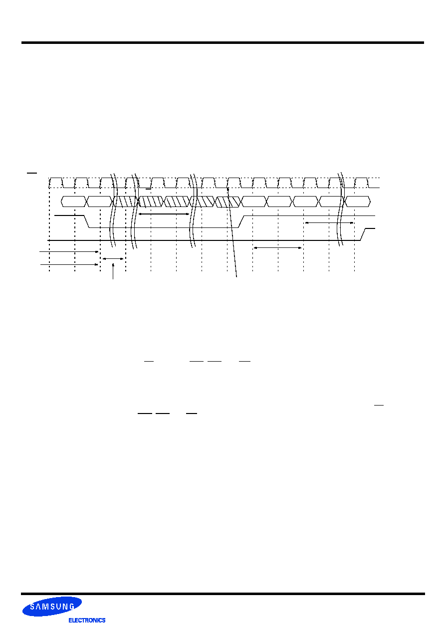
- 58 -
Rev 1.5 Oct. 2005
512M gDDR2 SDRAM
K4N51163QC-ZC
gDDR2 SDRAM input clock frequency can be changed under following condition :
gDDR2 SDRAM is in precharged power down mode. ODT must be turned off and CKE must be at logic LOW level. A minimum of 2
clocks must be waited after CKE goes LOW before clock frequency may change. SDRAM input clock frequency is allowed to change
only within minimum and maximum operating frequency specified for the particular speed grade. During input clock frequency change,
ODT and CKE must be held at stable LOW levels. Once input clock frequency is changed, stable new clocks must be provided to
DRAM before precharge power down may be exited and DLL must be RESET via EMRS after precharge power down exit. Depending
on new clock frequency an additional MRS command may need to be issued to appropriately set the WR, CL etc.. During DLL re-lock
period, ODT must remain off. After the DLL lock time, the DRAM is ready to operate with new clock frequency.
CK
CKE
T0
T4
Tx+1
Ty
Ty+1
Ty+2
T1
T2
Tx
CK
Valid
DLL
NOP
200 Clocks
Frequency Change
Ty+3
Tz
NOP
NOP
NOP
NOP
RESET
tRP
Clock Frequency Change in Precharge Power Down Mode
tXP
Occurs here
tAOFD
Stable new clock
before power down exit
ODT is off during
DLL RESET
Minimum 2 clocks
required before
changing frequency
ODT
CMD
Ty+4
No Operation Command
The No Operation Command should be used in cases when the gDDR2 SDRAM is in an idle or a wait state. The purpose of the No
Operation Command (NOP) is to prevent the gDDR2 SDRAM from registering any unwanted commands between operations. A No
Operation Command is registered when CS is low with RAS, CAS, and WE held high at the rising edge of the clock. A No Operation
Command will not terminate a previous operation that is still executing, such as a burst read or write cycle.
Deselect Command
The Deselect Command performs the same function as a No Operation Command. Deselect Command occurs when CS is brought
high at the rising edge of the clock, the RAS, CAS, and WE signals become don't cares.
Input Clock Frequency Change during Precharge Power Down

- 59 -
Rev 1.5 Oct. 2005
512M gDDR2 SDRAM
K4N51163QC-ZC
Note :
1. All gDDR2 SDRAM commands are defined by states of CS, RAS, CAS , WE and CKE at the rising edge of the clock.
2. Bank addresses BA0, BA1, BA2 (BA) determine which bank is to be operated upon. For (E)MRS BA selects an (Extended) Mode Register.
3. Burst reads or writes at BL=4 cannot be terminated or interrupted. See sections "Reads interrupted by a Read" and "Writes interrupted by a Write"
4. The Power Down Mode does not perform any refresh operations. The duration of Power Down is therefore limited by the refresh requirements outlined.
5. The state of ODT does not affect the states described in this table. The ODT function is not available during Self Refresh.
6. "X" means "H or L (but a defined logic level)".
7. Self refresh exit is asynchronous.
8. VREF must be maintained during Self Refresh operation.
Function
CKE
CS
RAS
CAS
WE
BA0
BA1
A11
A10
A9 - A0
Note
Previous
Cycle
Current
Cycle
(Extended) Mode Register Set
H
H
L
L
L
L
BA
OP Code
1,2
Refresh (REF)
H
H
L
L
L
H
X
X
X
X
1
Self Refresh Entry
H
L
L
L
L
H
X
X
X
X
1,8
Self Refresh Exit
L
H
H
X
X
X
X
X
X
X
1,7
L
H
H
H
Single Bank Precharge
H
H
L
L
H
L
BA
X
L
X
1,2
Precharge all Banks
H
H
L
L
H
L
X
X
H
X
1
Bank Activate
H
H
L
L
H
H
BA
Row Address
1,2
Write
H
H
L
H
L
L
BA
Column
L
Column
1,2,3
Write with Auto Precharge
H
H
L
H
L
L
BA
Column
H
Column
1,2,3
Read
H
H
L
H
L
H
BA
Column
L
Column
1,2,3
Read with Auto-Precharge
H
H
L
H
L
H
BA
Column
H
Column
1,2,3
No Operation
H
X
L
H
H
H
X
X
X
X
1
Device Deselect
H
X
H
X
X
X
X
X
X
X
1
Power Down Entry
H
L
H
X
X
X
X
X
X
X
1,4
L
H
H
H
Power Down Exit
L
H
H
X
X
X
X
X
X
X
1,4
L
H
H
H
Command Truth Table
- 60 -
Rev 1.5 Oct. 2005
512M gDDR2 SDRAM
K4N51163QC-ZC
Note :
1. CKE (N) is the logic state of CKE at clock edge N; CKE (N�1) was the state of CKE at the previous clock edge.
2. Current state is the state of the DDR SDRAM immediately prior to clock edge N.
3. COMMAND (N) is the command registered at clock edge N, and ACTION (N) is a result of COMMAND (N).
4. All states and sequences not shown are illegal or reserved unless explicitly described elsewhere in this document.
5. On Self Refresh Exit DESELECT or NOP commands must be issued on every clock edge occurring during the t
XSNR
period. Read commands may be
issued only after t
XSRD
(200 clocks) is satisfied.
6. Self Refresh mode can only be entered from the All Banks Idle state.
7. Must be a legal command as defined in the Command Truth Table.
8. Valid commands for Power Down Entry and Exit are NOP and DESELECT only.
9. Valid commands for Self Refresh Exit are NOP and DESELECT only.
10. Power Down and Self Refresh can not be entered while Read or Write operations, (Extended) Mode Register Set operations or Precharge operations
are in progress. See section "Power Down" and "Self Refresh Command" for a detailed list of restrictions.
11. Minimum CKE high time is three clocks.; minimum CKE low time is three clocks.
12. The state of ODT does not affect the states described in this table. The ODT function is not available during Self Refresh.
13. The Power Down does not perform any refresh operations. The duration of Power Down Mode is therefore limited by the refresh requirements outlined.
14. CKE must be maintained high while the SDRAM is in OCD calibration mode .
15. "X" means "don't care (including floating around VREF)" in Self Refresh and Power Down. However ODT must be driven high or low in Power Down if
the ODT function is enabled (Bit A2 or A6 set to "1" in EMRS(1) ).
16. V
REF
must be maintained during Self Refresh operation.
Current State
2
CKE
Command (N)
3
RAS, CAS, WE, CS
Action (N)
3
Note
Previous Cycle
1
(N-1)
Current Cycle
1
(N)
Power Down
L
L
X
Maintain Power-Down
11, 13, 15
L
H
DESELECT or NOP
Power Down Exit
4, 8, 11,13
Self Refresh
L
L
X
Maintain Self Refresh
11, 15
L
H
DESELECT or NOP
Self Refresh Exit
4, 5,9
Bank(s) Active
H
L
DESELECT or NOP
Active Power Down Entry
4,8,10,11,13
All Banks Idle
H
L
DESELECT or NOP
Precharge Power Down Entry
4, 8, 10,11,13
H
L
REFRESH
Self Refresh Entry
6, 9, 11,13
H
H
Refer to the Command Truth Table
7
DM Truth Table
Note :
1. Used to mask write data, provided coincident with the corresponding data
Name (Functional)
DM
DQs
Note
Write enable
-
Valid
1
Write inhibit
H
X
1
Clock Enable (CKE) Truth Table for Synchronous Transitions
- 61 -
Rev 1.5 Oct. 2005
512M gDDR2 SDRAM
K4N51163QC-ZC
AC Overshoot/Undershoot Specification for Address and Control Pins A0-A15, BA0-BA2, CS, RAS, CAS, WE, CKE, ODT
AC Overshoot/Undershoot Specification for Clock, Data, Strobe, and Mask Pins DQ, DQS, DM, CK, CK
Parameter
Specification
- 36
- 2A
Maximum peak amplitude allowed for overshoot area (See following figyre):
0.9V
0.9V
Maximum peak amplitude allowed for undershoot area (See following figure):
0.9V
0.9V
Maximum overshoot area above VDD (See following figure).
0.56 V-ns
0.45 V-ns
Maximum undershoot area below VSS (See following figure).
0.56 V-ns
0.45 V-ns
Parameter
Specification
- 36
-2A
Maximum peak amplitude allowed for overshoot area (See following figure):
0.9V
0.9V
Maximum peak amplitude allowed for undershoot area (See following figure):
0.9V
0.9V
Maximum overshoot area above VDDQ (See following figure):
0.28 V-ns
0.23 V-ns
Maximum undershoot area below VSSQ (See following figure):
0.28 V-ns
0.23 V-ns
Overshoot Area
Maximum Amplitude
V
DD
Undershoot Area
Maximum Amplitude
V
SS
Volts
(V)
AC Overshoot and Undershoot Definition for Address and Control Pins
Time (ns)
Overshoot Area
Maximum Amplitude
V
DDQ
Undershoot Area
Maximum Amplitude
V
SSQ
Volts
(V)
AC Overshoot and Undershoot Definition for Clock, Data, Strobe, and Mask Pins
Time (ns)
Input Signal Overshoot/Undershoot Specification
- 62 -
Rev 1.5 Oct. 2005
512M gDDR2 SDRAM
K4N51163QC-ZC
Table 1. Full Strength Default Pulldown Driver Characteristics
Pulldown Current (mA)
Voltage (V)
Minimum
(23.4 Ohms)
Nominal Default Low (18
ohms)
Nominal Default High(18
ohms)
Maximum
(12.6 Ohms)
0.2
8.5
11.3
11.8
15.9
0.3
12.1
16.5
16.8
23.8
0.4
14.7
21.2
22.1
31.8
0.5
16.4
25.0
27.6
39.7
0.6
17.8
28.3
32.4
47.7
0.7
18.6
30.9
36.9
55.0
0.8
19.0
33.0
40.9
62.3
0.9
19.3
34.5
44.6
69.4
1.0
19.7
35.5
47.7
75.3
1.1
19.9
36.1
50.1
80.5
1.2
20.0
36.6
52.2
84.6
1.3
20.1
36.9
54.2
87.7
1.4
20.2
37.1
55.9
90.8
1.5
20.3
37.4
57.1
92.9
1.6
20.4
37.6
58.4
94.9
1.7
20.6
37.7
59.6
97.0
1.8
37.9
60.9
99.1
1.9
101.1
0.2
0.3
0.4
0.5
0.6
0.7
0.8
0.9
1.0
1.1
1.2
1.3
1.4
1.5
1.6
1.7
1.8
1.9
VOUT to VSSQ (V)
0
20
40
60
80
100
120
Pulldown current (mA)
Maximum
Nominal
Default
High
Nominal
Default
Low
Minimum
Figure 1. gDDR2 Default Pulldown Characteristics for Full Strength Driver

- 63 -
Rev 1.5 Oct. 2005
512M gDDR2 SDRAM
K4N51163QC-ZC
Table 2. Full Strength Default Pullup Driver Characteristics
Pulldown Current (mA)
Voltage (V)
Minimum
(23.4 Ohms)
Nominal Default Low (18
ohms)
Nominal Default High(18
ohms)
Maximum
(12.6 Ohms)
0.2
-8.5
-11.1
-11.8
-15.9
0.3
-12.1
-16.0
-17.0
-23.8
0.4
-14.7
-20.3
-22.2
-31.8
0.5
-16.4
-24.0
-27.5
-39.7
0.6
-17.8
-27.2
-32.4
-47.7
0.7
-18.6
-29.8
-36.9
-55.0
0.8
-19.0
-31.9
-40.8
-62.3
0.9
-19.3
-33.4
-44.5
-69.4
1.0
-19.7
-34.6
-47.7
-75.3
1.1
-19.9
-35.5
-50.4
-80.5
1.2
-20.0
-36.2
-52.5
-84.6
1.3
-20.1
-36.8
-54.2
-87.7
1.4
-20.2
-37.2
-55.9
-90.8
1.5
-20.3
-37.7
-57.1
-92.9
1.6
-20.4
-38.0
-58.4
-94.9
1.7
-20.6
-38.4
-59.6
-97.0
1.8
-38.6
-60.8
-99.1
1.9
-101.1
0.2
0.3
0.4
0.5
0.6
0.7
0.8
0.9
1.0
1.1
1.2
1.3
1.4
1.5
1.6
1.7
1.8
1.9
VDDQ to VOUT (V)
-120
-100
-80
-60
-40
-20
0
Pullup current (mA)
Minimum
Nominal
Default
Low
Nominal
Default
High
Maximum
Figure 2. gDDR2 Default Pullup Characteristics for Full Strength Output Driver
- 64 -
Rev 1.5 Oct. 2005
512M gDDR2 SDRAM
K4N51163QC-ZC
gDDR2 SDRAM Default Output Driver V�I Characteristics
gDDR2 SDRAM output driver characteristics are defined for full strength default operation as selected by the EMRS1 bits A7-A9 = `111'.
Figures 1 and 2 show the driver characteristics graphically, and tables 1 and 2 show the same data in tabular format suitable for input
into simulation tools. The driver characteristics evaluation conditions are:
Nominal Default 25
o
C (T case), VDDQ = 1.8 V, typical process
Minimum TBD
o
C (T case), VDDQ = 1.7 V, slow�slow process
Maximum 0
o
C (T case), VDDQ = 1.9 V, fast�fast process
Default Output Driver Characteristic Curves Notes:
1) The full variation in driver current from minimum to maximum process, temperature, and voltage will lie within the outer bounding lines
of the V�I curve of figures 1 and 2.
2) It is recommended that the "typical" IBIS V�I curve lie within the inner bounding lines of the V�I curves of figures 1 and 2.
Table 3. Full Strength Calibrated Pulldown Driver Characteristics
Table 4. Full Strength Calibrated Pullup Driver Characteristics
gDDR2 SDRAM Calibrated Output Driver V�I Characteristics
gDDR2 SDRAM output driver characteristics are defined for full strength calibrated operation as selected by the procedure outlined in
Off-Chip Driver (OCD) Impedance Adjustment. Tables 3 and 4 show the data in tabular format suitable for input into simulation tools. The
nominal points represent a device at exactly 18 ohms. The nominal low and nominal high values represent the range that can be
achieved with a maximum 1.5 ohm step size with no calibration error at the exact nominal conditions only (i.e. perfect calibration proce-
dure, 1.5 ohm maximum step size guaranteed by specification). Real system calibration error needs to be added to these values. It
must be understood that these V-I curves as represented here or in supplier IBIS models need to be adjusted to a wider range as a
result of any system calibration error. Since this is a system specific phenomena, it cannot be quantified here. The values in the cali-
brated tables represent just the DRAM portion of uncertainty while looking at one DQ only. If the calibration procedure is used, it is pos-
sible to cause the device to operate outside the bounds of the default device characteristics tables and figures. In such a situation, the
timing parameters in the specification cannot be guaranteed. It is solely up to the system application to ensure that the device is cali-
brated between the minimum and maximum default values at all times. If this can't be guaranteed by the system calibration procedure,
re-calibration policy, and uncertainty with DQ to DQ variation, then it is recommended that only the default values be used. The nominal
maximum and minimum values represent the change in impedance from nominal low and high as a result of voltage and temperature
change from the nominal condition to the maximum and minimum conditions. If calibrated at an extreme condition, the amount of varia-
tion could be as much as from the nominal minimum to the nominal maximum or vice versa. The driver characteristics evaluation condi-
tions are:
Nominal 25
o
C (T case), VDDQ = 1.8 V, typical process.
Nominal Low and Nominal High 25
o
C (T case), VDDQ = 1.8 V, any process.
Nominal Minimum TBD
o
C (T case), VDDQ = 1.7 V, any process.
Nominal Maximum 0
o
C (T case), VDDQ = 1.9 V, any process.
Calibrated Pulldown Current (mA)
Voltage (V)
Nominal Minimum
(21 Ohms)
Nominal Low
(18.75 ohms)
Nominal
(18 ohms)
Nominal High
(17.25 ohms)
Nominal Maximum
(15 Ohms)
0.2
9.5
10.7
11.5
11.8
13.3
0.3
14.3
16.0
16.6
17.4
20.0
0.4
18.7
21.0
21.6
23.0
27.0
Calibrated Pulldown Current (mA)
Voltage (V)
Nominal Minimum
(21 Ohms)
Nominal Low
(18.75 ohms)
Nominal
(18 ohms)
Nominal High
(17.25 ohms)
Nominal Maximum
(15 Ohms)
0.2
-9.5
-10.7
-11.4
-11.8
-13.3
0.3
-14.3
-16.0
-16.5
-17.4
-20.0
0.4
-18.7
-21.0
-21.2
-23.0
-27.0