Äîêóìåíòàöèÿ è îïèñàíèÿ www.docs.chipfind.ru
- 1 -
Rev 1.6 (Apr. 2005)
256M gDDR2 SDRAM
K4N56163QF-GC
256Mbit gDDR2 SDRAM
Revision 1.6
April 2005
Samsung Electronics reserves the right to change products or specification without notice.
INFORMATION IN THIS DOCUMENT IS PROVIDED IN RELATION TO SAMSUNG PRODUCTS,
AND IS SUBJECT TO CHANGE WITHOUT NOTICE.
NOTHING IN THIS DOCUMENT SHALL BE CONSTRUED AS GRANTING ANY LICENSE,
EXPRESS OR IMPLIED, BY ESTOPPEL OR OTHERWISE,
TO ANY INTELLECTUAL PROPERTY RIGHTS IN SAMSUNG PRODUCTS OR TECHNOLOGY. ALL
INFORMATION IN THIS DOCUMENT IS PROVIDED
ON AS "AS IS" BASIS WITHOUT GUARANTEE OR WARRANTY OF ANY KIND.
1. For updates or additional information about Samsung products, contact your nearest Samsung office.
2. Samsung products are not intended for use in life support, critical care, medical, safety equipment, or similar
applications where Product failure could result in loss of life or personal or physical harm, or any military or
defense application, or any governmental procurement to which special terms or provisions may apply.

- 2 -
Rev 1.6 (Apr. 2005)
256M gDDR2 SDRAM
K4N56163QF-GC
Revision History
Revision 1.6 (April 14, 2005)
· Modified Power-up and Initialization Sequence on page 22.
Revision 1.5 (March 04, 2005)
· Removed K4N56163QF-GC20/22 from the datasheet
Revision 1.4 (February 5, 2005)
· Added Lead-Free part number in the datasheet.
Revision 1.3 (January 5, 2005)
· Typo corrected
Revision 1.2 (December 28, 2004)
· Changed the DC characteristics table
· Added 50 ohm at the EMRS(1) programming table.
Revision 1.1 (December 1, 2004)
· Changed ICC2P and ICC6 to 10mA
Revision 1.0 (October 20, 2004)
· DC spec defined.
· Changed VDD&VDDQ of K4N56163QF-GC20/22 from 1.8V+0.1V to 2.0V+0.1V
Revision 0.0 (April 29, 2004)
- Target Spec
· Defined Target Specification
- 3 -
Rev 1.6 (Apr. 2005)
256M gDDR2 SDRAM
K4N56163QF-GC
· 1.8V + 0.1V power supply for device operation
· 1.8V + 0.1V power supply for I/O interface
· 4 Banks operation
· Posted CAS
· Programmable CAS Letency : 4, 5, 6 and 7
· Programmable Additive Latency : 0, 1, 2, 3, 4 and 5
· Write Latency (WL) = Read Latency (RL) -1
· Burst Legth : 4 and 8 (Interleave/nibble sequential)
· Programmable Sequential/ Interleave Burst Mode
GENERAL DESCRIPTION
FEATURES
· Bi-directional Differential Data-Strobe
(Single-ended data-strobe is an optional feature)
· Off-chip Driver (OCD) Impedance Adjustment
· On Die Termination
· Refresh and Self Refresh
Average Refesh Period 7.8us at lower then T
CASE
85×C,
3.9us at 85×C < T
CASE
< 95 ×C
· 84 ball FBGA
4M x 16Bit x 4 Banks graphic DDR2 Synchronous DRAM
with Differential Data Strobe
ORDERING INFORMATION
* K4N56163QF-ZC is the Lead-Free part number.
Part NO.
Max Freq.
Max Data Rate
Interface
Package
K4N56163QF-GC25
400MHz
800Mbps/pin
SSTL
84 Ball FBGA
K4N56163QF-GC30
333MHz
667Mbps/pin
K4N56163QF-GC37
266MHz
533Mbps/pin
The 256Mb gDDR2 SDRAM chip is organized as 4Mbit x 16 I/O x 4banks banks device. This synchronous device
achieve high speed graphic double-data-rate transfer rates of up to 1000Mb/sec/pin for general applications. The chip is
designed to comply with the following key gDDR2 SDRAM features such as posted CAS with additive latency, write latency
= read latency - 1, Off-Chip Driver(OCD) impedance adjustment and On Die Termination.
All of the control and address inputs are synchronized with a pair of externally supplied differential clocks. Inputs are
latched at the cross point of differential clocks (CK rising and CK falling). All I/Os are synchronized with a pair of bidirec-
tional strobes (DQS and DQS) in a source synchronous fashion. A thirteen bit address bus is used to convey row, column,
and bank address information in a RAS/CAS multiplexing style. For example, 256Mb(x16) device receive 13/9/2 address-
ing. The 256Mb gDDR2 devices operate with a single 1.8V ± 0.1V power supply and 1.8V ± 0.1V VDDQ.
The 256Mb gDDR2 devices are available in 84ball FBGAs(x16).
Note : The functionality described and the timing specifications included in this data sheet are for the DLL Enabled mode of
operation.
FOR 4M x 16Bit x 4 Bank gDDR2 SDRAM
- 4 -
Rev 1.6 (Apr. 2005)
256M gDDR2 SDRAM
K4N56163QF-GC
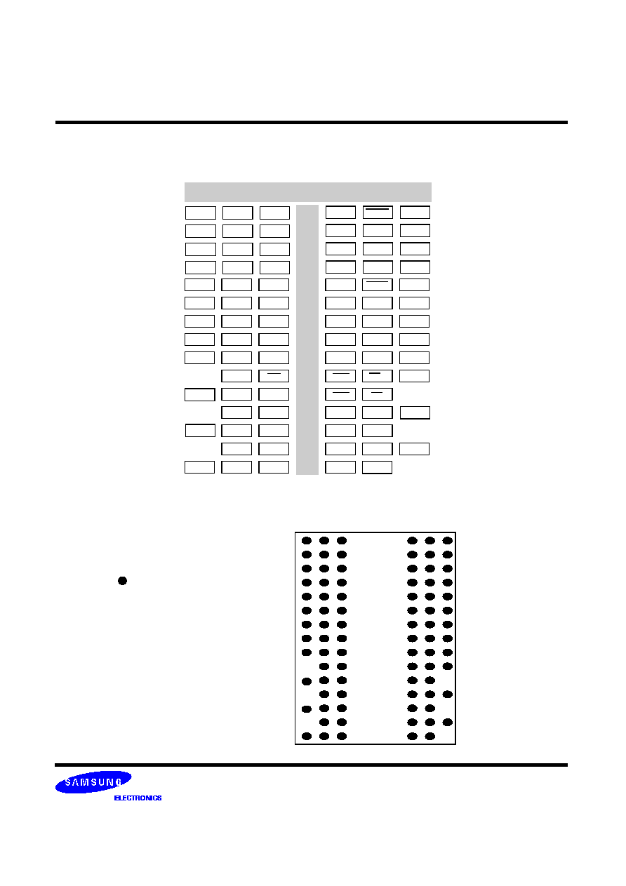
PIN CONFIGURATION
Normal Package (Top View)
A
B
C
D
E
F
G
H
J
K
L
VDD
NC
VSS
LDQ6
VSSQ
LDM
VDDQ
VDDQ
VDDQ
VSSQ
VSSQ
LDQS
LDQS
LDQ7
LDQ0
VDDQ
LDQ2
VSSQ
LDQ5
VSSDL
VDD
CK
RAS
CK
CAS
CS
A2
A6
A4
A11
A8
NC
NC
NC
A12
A9
A7
A5
A0
VDD
A10
VSS
VDDQ
VSSQ
LDQ1
LDQ3
LDQ4
VDDL
A1
A3
BA1
VREF
VSS
CKE
WE
BA0
1 2 3 7 8 9
VDD
VSS
VDD
NC
VSS
UDQ6
VSSQ
UDM
VDDQ
VDDQ
VSSQ
UDQ1
UDQ3
UDQ4
VDDQ
VDDQ
VSSQ
VSSQ
UDQS
UDQS
UDQ7
UDQ0
VDDQ
UDQ2
VSSQ
UDQ5
NC
ODT
M
N
P
R
Notes:
VDDL and VSSDL are power and ground for the DLL. lt is recommended that they are isolated on the device from VDD,
VDDQ, VSS, and VSSQ.
+
+
+
+
+
+
+
+
+
+
+
1
2
3
4
5
6
7
8
9
A
B
C
D
E
F
G
H
J
K
L
+
+
+
+
+
+
+
+
+
+
+
+
+
+
+
+
+
+
+
+
+
+
+
+
+
+
+
+
+
+
+
+
+
+
M
N
P
R
+
+
+
+
+
+
: Populated Ball
+ : Depopulated Ball
Top View
Ball Locations
(See the balls through the Package)
- 5 -
Rev 1.6 (Apr. 2005)
256M gDDR2 SDRAM
K4N56163QF-GC
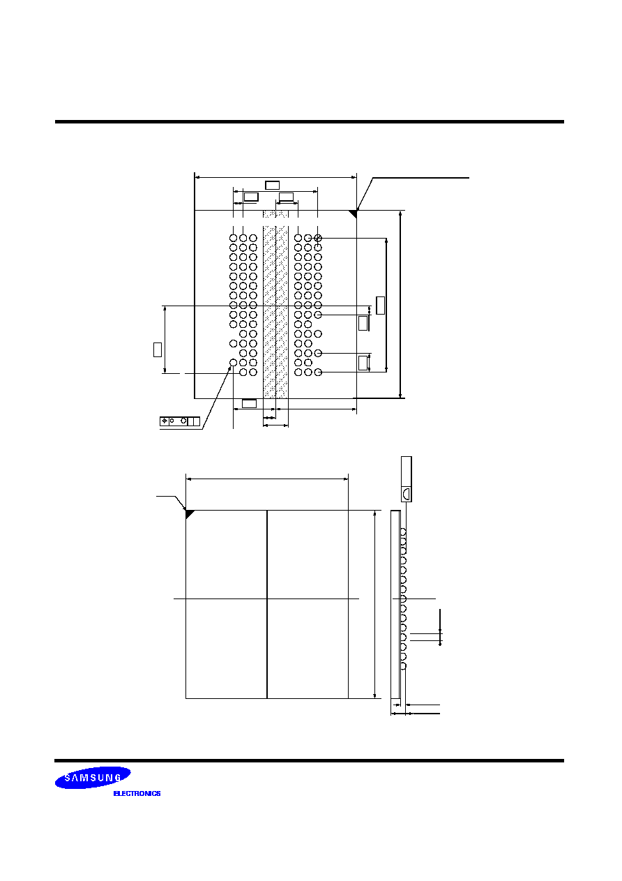
PACKAGE DIMENSIONS (84 Ball FBGA)
Unit : mm
13
.00
±
0.10
11
.
2
0
0.8
0
1.
60
11.00
±
0.10
1
2
3
4
5
6
7
8
9
6.40
0.80
1.60
B
C
D
E
F
G
H
J
K
L
A
5.
6
0
(6.15)
(0.90)
(1.80)
3.20
84-
0.45
±
0.05
0.2
M A B
13
.00
±
0.1
0
11.00
±
0.10
#A1
0.50
±
0.0
5
0.
10M
A
X
0.35
±
0.05
MAX.1.20
M
N
P
R
# A1 INDEX MARK (OPTIONAL)