CMOS DRAM
K4P170411C, K4P160411C
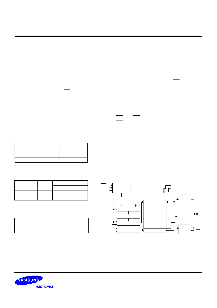
This is a family of 4,194,304 x 4 bit Quad CAS with Fast Page Mode CMOS DRAMs. Fast Page Mode offers high speed random access
of memory cells within the same row. Refresh cycle (2K Ref. or 4K Ref.), access time (-50 or -60), power consumption(Normal or Low
power) and package type(SOJ or TSOP-II) are optional features of this family. All of this family have CAS-before-RAS refresh, RAS-only
refresh and Hidden refresh capabilities. Furthermore, Self-refresh operation is available in L-version. Four separate CAS pins provide for
seperate I/O operation allowing this device to operate in parity mode.
This 4Mx4 Fast Page Mode Quad CAS DRAM family is fabricated using Samsung
s advanced CMOS process to realize high band-
width, low power consumption and high reliability.
∑
Part Identification
- K4P170411C-B(F) (5V, 4K Ref.)
- K4P160411C-B(F) (5V, 2K Ref.)
∑
Fast Page Mode operation
∑
Four seperate CAS pins provide for separate I/O operation
∑
CAS-before-RAS refresh capability
∑
RAS-only and Hidden refresh capability
∑
Self-refresh capability (L-ver only)
∑
Fast paralleltest mode capability
∑
TTL compatible inputs and outputs
∑
Early Write or output enable controlled write
∑
JEDEC Standard pinout
∑
Available in Plastic SOJ and TSOP(II) packages
∑
Single +5V
±
10% power supply
Control
Clocks
RAS
CAS0 - 3
W
Vcc
Vss
DQ0
to
DQ3
A0-A11
(A0 - A10)
*1
A0 - A9
(A0 - A10)
*1
Memory Array
4,194,304 x 4
Cells
SAMSUNG ELECTRONICS CO., LTD. reserves the right to
change products and specifications without notice.
4M x 4Bit CMOS Quad CAS DRAM with Fast Page Mode
DESCRIPTION
FEATURES
FUNCTIONAL BLOCK DIAGRAM
∑
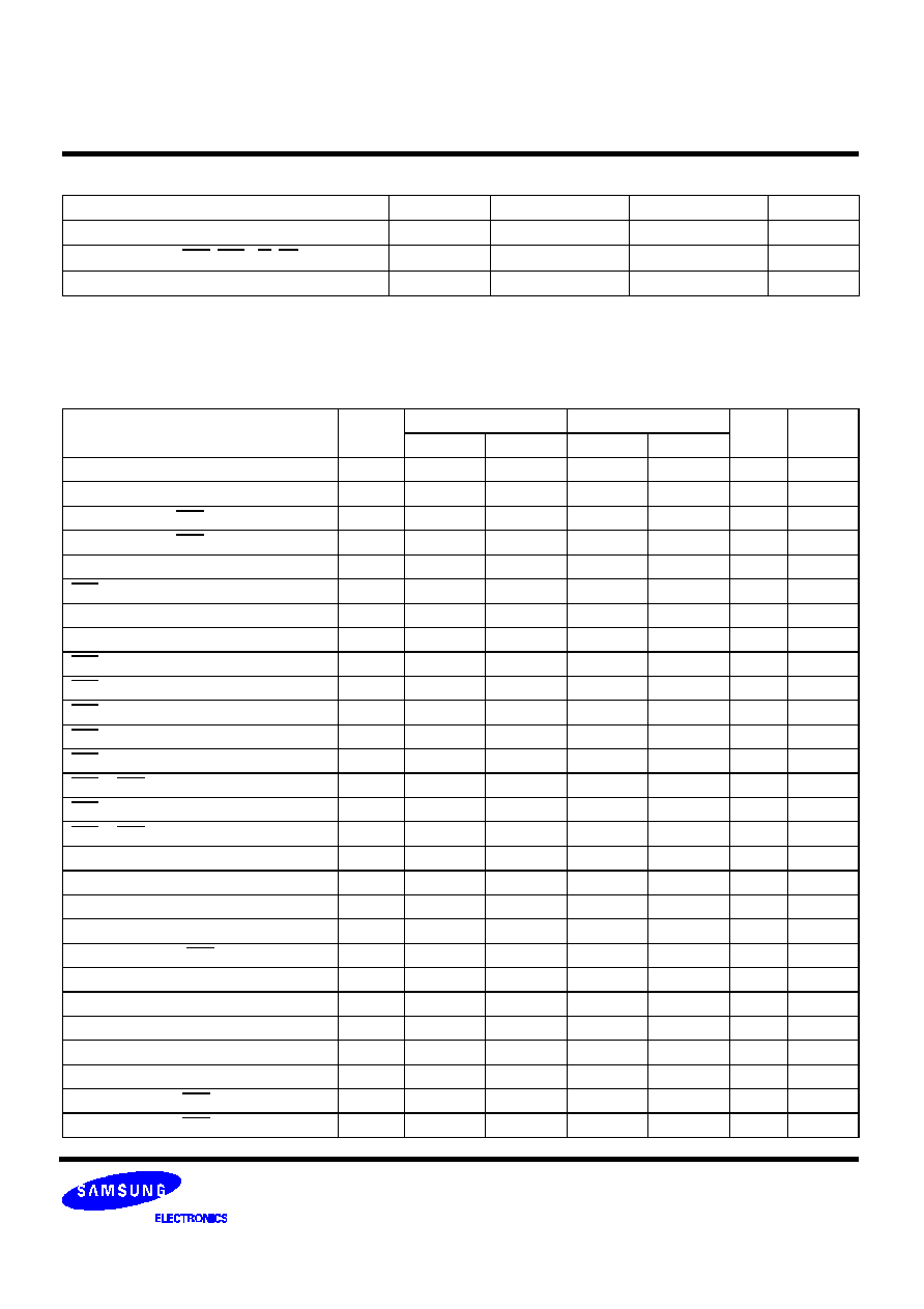
Refresh Cycles
Part
NO.
Refresh
cycle
Refresh period
Normal
L-ver
K4P170411C
4K
64ms
128ms
K4P160411C
2K
32ms
∑
Performance Range
Speed
t
RAC
t
CAC
t
RC
t
PC
Remark
-50
50ns
13ns
90ns
35ns
5V/3.3V
-60
60ns
15ns
110ns
40ns
5V/3.3V
∑ Active Power Dissipation
Speed
Refresh Cycle
4K
2K
-50
495
605
-60
440
550
Unit : mW
S
e
n
s
e
A
m
p
s
&
I
/
O
Data out
Buffer
Data in
Buffer
OE
Note)
*1
: 2K Refresh
Col. Address Buffer
Row Address Buffer
Refresh Counter
Refresh Control
Refresh Timer
Column Decoder
Row Decoder
VBB Generator
CMOS DRAM
K4P170411C, K4P160411C
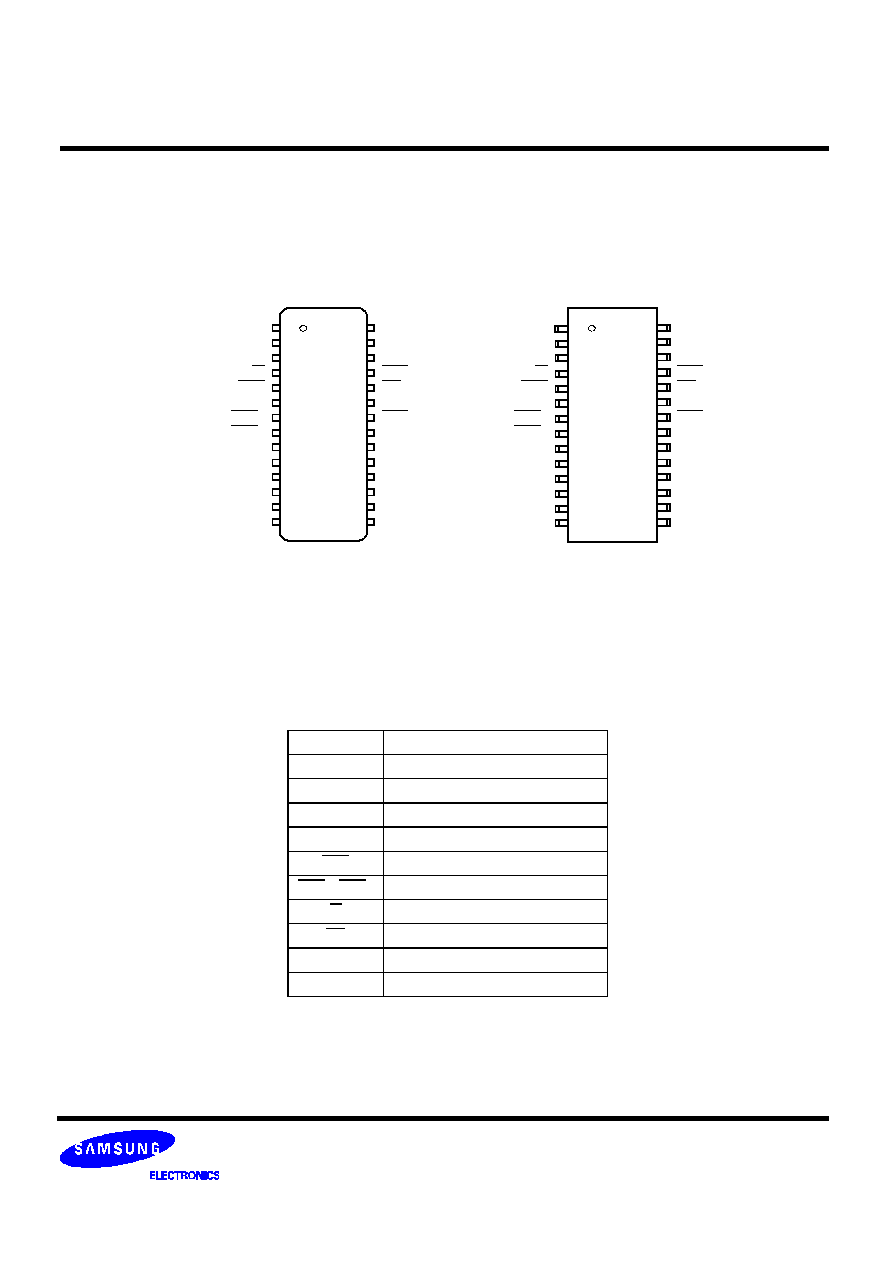
PIN CONFIGURATION (Top Views)
Pin Name
Pin Function
A0 - A11
Address Inputs (4K Product)
A0 - A10
Address Inputs (2K Product)
DQ0 - 3
Data In/Out
V
SS
Ground
RAS
Row Address Strobe
CAS0~CAS3
Column Address Strobe
W
Read/Write Input
OE
Data Output Enable
V
CC
Power(+5.0V)
N.C
No Connection
V
CC
DQ0
DQ1
W
RAS
*A11(N.C)
CAS0
CAS1
A10
A0
A1
A2
A3
V
CC
V
SS
DQ3
DQ2
CAS3
OE
A9
CAS2
N.C
A8
A7
A6
A5
A4
V
SS
1
2
3
4
5
6
7
8
9
10
11
12
13
14
28
27
26
25
24
23
22
21
20
19
18
17
16
15
V
CC
DQ0
DQ1
W
RAS
*A11(N.C)
CAS0
CAS1
A10
A0
A1
A2
A3
V
CC
V
SS
DQ3
DQ2
CAS3
OE
A9
CAS2
N.C
A8
A7
A6
A5
A4
V
SS
1
2
3
4
5
6
7
8
9
10
11
12
13
14
28
27
26
25
24
23
22
21
20
19
18
17
16
15
*A11 is N.C for K4P160411C(5V, 2K Ref. product)
B : 300mil 28 SOJ
F : 300mil 28 TSOP II
∑ K4P17(6)0411C-B
∑ K4P17(6)0411C-F
CMOS DRAM
K4P170411C, K4P160411C
ABSOLUTE MAXIMUM RATINGS
* Permanent device damage may occur if "ABSOLUTE MAXIMUM RATINGS" are exceeded. Functional operation should be restricted
to the conditions as detailed in the operational sections of this data sheet. Exposure to absolute maximum rating conditions for
extended periods may affect device reliability.
Parameter
Symbol
Rating
Units
Voltage on any pin relative to V
SS
V
IN,
V
OUT
-1.0 to +7.0
V
Voltage on V
CC
supply relative to V
SS
V
CC
Inputs
-1.0 to +7.0
V
Storage Temperature
Tstg
-55 to +150
∞
C
Power Dissipation
P
D
1
W
Short Circuit Output Current
I
OS
50
mA
RECOMMENDED OPERATING CONDITIONS
(Voltage referenced to Vss, T
A
= 0 to 70
∞
C)
*1 : V
CC
+2.0V/20ns, Pulse width is measured at V
CC
*2 : -2.0/20ns, Pulse width is measured at V
SS
Parameter
Symbol
Min
Typ
Max
Units
Supply Voltage
V
CC
4.5
5.0
5.5
V
Ground
V
SS
0
0
0
V
Input High Voltage
V
IH
2.4
-
V
CC
+1.0
*1
V
Input Low Voltage
V
IL
-1.0
*2
-
0.8
V
DC AND OPERATING CHARACTERISTICS
(Recommended operating conditions unless otherwise noted.)
Parameter
Symbol
Min
Max
Units
Input Leakage Current (Any input 0
V
IN
V
IN
+0.5V,
all other input pins not under test=0 Volt)
I
I(L)
-5
5
uA
Output Leakage Current
(Data out is disabled, 0V
V
OUT
V
CC
)
I
O(L)
-5
5
uA
Output High Voltage Level(I
OH
=-5mA)
V
OH
2.4
-
V
Output Low Voltage Level(I
OL
=4.2mA)
V
OL
-
0.4
V
CMOS DRAM
K4P170411C, K4P160411C
*Note :
I
CC1
, I
CC3
, I
CC4
and I
CC6
are dependent on output loading and cycle rates. Specified values are obtained with the output open.
I
CC
is specified as an average current. In I
CC1
, I
CC3
and I
CC6
address can be changed maximum once while RAS=V
IL
. In I
CC4
,
address can be changed maximum once within one fast page mode cycle time, t
PC
.
DC AND OPERATING CHARACTERISTICS
(Continued)
I
CC1
* : Operating Current (RAS and CAS, Address cycling @t
RC
=min.)
I
CC2
: Standby Current (RAS=CAS=W=V
IH
)
I
CC3
* : RAS-only Refresh Current (CAS=V
IH
, RAS, Address cycling @t
RC
=min.)
I
CC4
* : Fast Page Mode Current (RAS=V
IL
, CAS, Address cycling @t
PC
=min.)
I
CC5
: Standby Current (RAS=CAS=W=V
CC
-0.2V)
I
CC6
* : CAS-Before-RAS Refresh Current (RAS and CAS cycling @t
RC
=min.)
I
CC7
: Battery back-up current, Average power supply current, Battery back-up mode
Input high voltage(V
IH
)=V
CC
-0.2V, Input low voltage(V
IL
)=0.2V, CAS=0.2V,
DQ=Don
t care, T
RC
=31.25us(4K/L-ver), 62.5us(2K/L-ver), T
RAS
=T
RAS
min~300ns
I
CCS
: Self Refresh Current
RAS=CAS=0.2V, W=OE=A0 ~ A11=V
CC
-0.2V or 0.2V,
DQ0 ~ DQ3=V
CC
-0.2V, 0.2V or Open
Symbol
Power
Speed
Max
Units
K4P170411C
K4P160411C
I
CC1
Don
t care
-50
-60
90
80
110
100
mA
mA
mA
I
CC2
Normal
L
Don
t care
2
1
2
1
mA
mA
I
CC3
Don
t care
-50
-60
90
80
110
100
mA
mA
mA
I
CC4
Don
t care
-50
-60
80
70
90
80
mA
mA
mA
I
CC5
Normal
L
Don
t care
1
250
1
250
mA
uA
I
CC6
Don
t care
-50
-60
90
80
110
100
mA
mA
mA
I
CC7
L
Don
t care
300
300
uA
I
CCS
L
Don
t care
250
250
uA
CMOS DRAM
K4P170411C, K4P160411C
CAPACITANCE
(T
A
=25
∞
C, V
CC
=5V, f=1MHz)
Parameter
Symbol
Min
Max
Units
Input capacitance [A0 ~ A11]
C
IN1
-
5
pF
Input capacitance [RAS, CASx, W, OE]
C
IN2
-
7
pF
Output capacitance [DQ0 - DQ3]
C
DQ
-
7
pF
Test condition : V
CC
=5.0V
±
10%, Vih/Vil=2.4/0.8V, Voh/Vol=2.4/0.4V
Parameter
Symbol
-50
-60
Units
Notes
Min
Max
Min
Max
Random read or write cycle time
t
RC
90
110
ns
Read-modify-write cycle time
t
RWC
133
155
ns
Access time from RAS
t
RAC
50
60
ns
3,4,10
Access time from CAS
t
CAC
13
15
ns
3,4,5,18
Access time from column address
t
AA
25
30
ns
3,10
CAS to output in Low-Z
t
CLZ
0
0
ns
3,18
Output buffer turn-off delay
t
OFF
0
13
0
15
ns
6
Transition time (rise and fall)
t
T
3
50
3
50
ns
2
RAS precharge time
t
RP
30
40
ns
RAS pulse width
t
RAS
50
10K
60
10K
ns
RAS hold time
t
RSH
13
15
ns
14
CAS hold time
t
CSH
50
60
ns
17
CAS pulse width
t
CAS
13
10K
15
10K
ns
23
RAS to CAS delay time
t
RCD
20
37
20
45
ns
4,16
RAS to column address delay time
t
RAD
15
25
15
30
ns
10
CAS to RAS precharge time
t
CRP
5
5
ns
15
Row address set-up time
t
ASR
0
0
ns
Row address hold time
t
RAH
10
10
ns
Column address set-up time
t
ASC
0
0
ns
16
Column address hold time
t
CAH
10
10
ns
16
Column address to RAS lead time
t
RAL
25
30
ns
Read command set-up time
t
RCS
0
0
ns
Read command hold time referenced to
t
RCH
0
0
ns
8,15
Read command hold time referenced to
t
RRH
0
0
ns
8
Write command hold time
t
WCH
10
10
ns
14
Write command pulse width
t
WP
10
10
ns
Write command to RAS lead time
t
RWL
13
15
ns
Write command to CAS lead time
t
CWL
13
15
ns
17
AC CHARACTERISTICS
(0
∞
C
T
A
70
∞
C, See note 1,2)