Page 1
Direct RDRAM
TM
K4R271669F
Version 1.4 Sept. 2003
Overview
The Rambus Direct RDRAMTMis a general purpose high-
performance memory device suitable for use in a broad
range of applications including communications, graphics,
video, and any other application where high bandwidth and
low latency are required.
The 128Mbit Direct Rambus DRAMs (RDRAM
) are
extremely high-speed CMOS DRAMs organized as 8M
words by 16. The use of Rambus Signaling Level (RSL)
technology permits to 800MHz transfer rates while using
conventional system and board design technologies. Direct
RDRAM devices are capable of sustained data transfers at
1.25 ns per two bytes (10ns per sixteen bytes).
The architecture of the Direct RDRAMs allows the highest
sustained bandwidth for multiple, simultaneous randomly
addressed memory transactions. The separate control and
data buses with independent row and column control yield
over 95% bus efficiency. The Direct RDRAM's 32 banks
support up to four simultaneous transactions.
System oriented features for mobile, graphics and communi-
cations include power management, byte masking.
Features
Highest sustained bandwidth per DRAM device
- 1.6GB/s sustained data transfer rate
- Separate control and data buses for maximized
efficiency
- Separate row and column control buses for
easy scheduling and highest performance
- 32 banks: four transactions can take place simul-
taneously at full bandwidth data rates
Low latency features
- Write buffer to reduce read latency
- 3 precharge mechanisms for controller flexibility
- Interleaved transactions
Advanced power management:
- Multiple low power states allows flexibility in power
consumption versus time to transition to active state
- Power-down self-refresh
Organization: 1Kbyte pages and 32 banks
Uses Rambus Signaling Level (RSL) interface
for up
to 800MHz operation
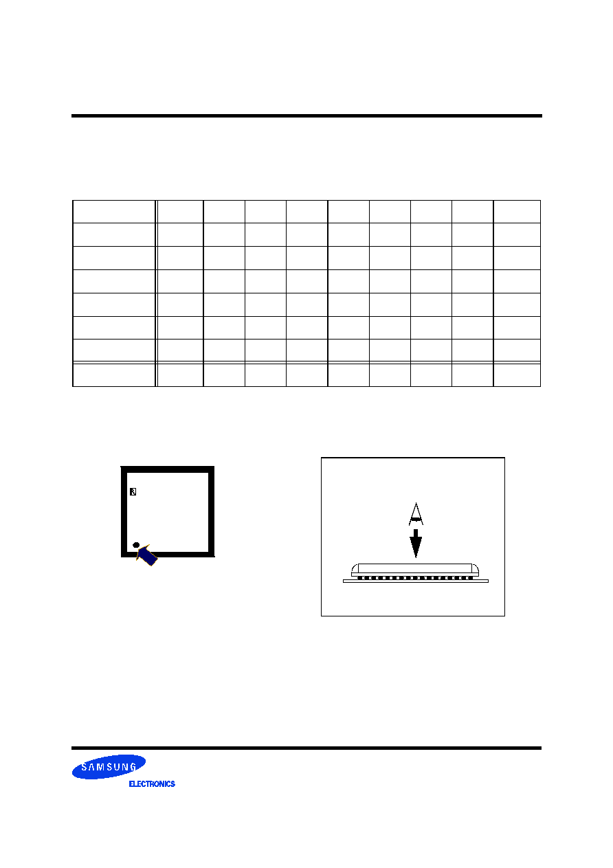
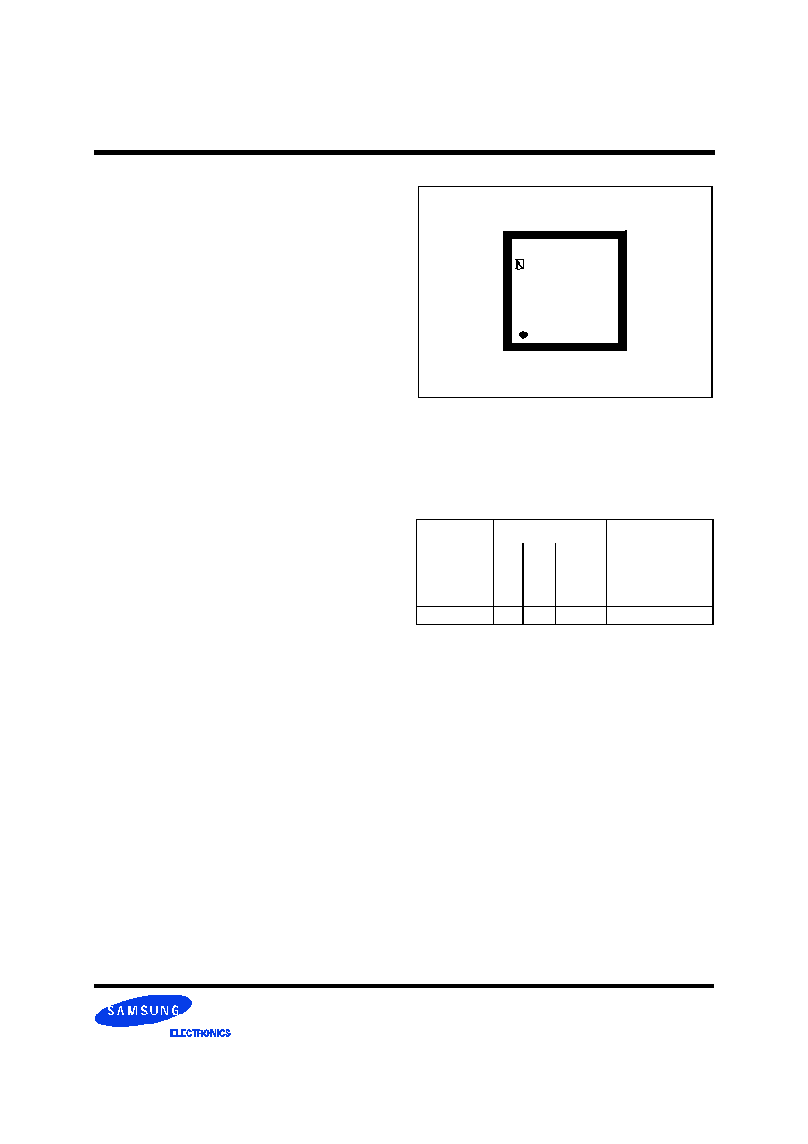
WBGA package(54 Balls)
The 128Mbit Direct RDRAMs are offered in a horizontal
center-bond fanout CSP.
Key Timing Parameters/Part Numbers
Figure 1: Direct RDRAM CSP Package
Organization
Speed
Part Number
Bin
I/O
Freq.
MHz
t
RAC
(Row
Access
Time) ns
256Kx16x32s
a
a.
"
32s
"
- 32 banks which use a
"
split
"
bank architecture.
-CS8
800
45
K4R271669F-T
b
CS8
b.
"
T
"
- Lead free consumer package.
K4R271669F
SEC 340 TCS8
Page 3
Direct RDRAM
TM
K4R271669F
Version 1.4 Sept. 2003
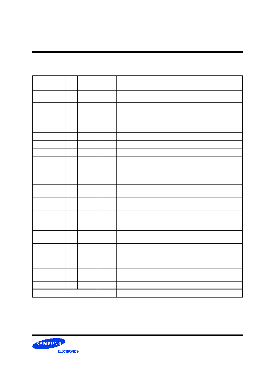
Table 2: Pin Description
Signal
I/O
Type
# Pins
center
Description
SIO1,SIO0
I/O
CMOS
a
2
Serial input/output. Pins for reading from and writing to the control regis-
ters using a serial access protocol. Also used for power management.
CMD
I
CMOS
a
1
Command input. Pins used in conjunction with SIO0 and SIO1 for reading
from and writing to the control registers. Also used for power manage-
ment.
SCK
I
CMOS
a
1
Serial clock input. Clock source used for reading from and writing to the
control registers
V
DD
6
Supply voltage for the RDRAM core and interface logic.
V
DDa
1
Supply voltage for the RDRAM analog circuitry.
V
CMOS
2
Supply voltage for CMOS input/output pins.
GND
9
Ground reference for RDRAM core and interface.
GNDa
1
Ground reference for RDRAM analog circuitry.
DQA7..DQA0
I/O
RSL
b
8
Data byte A. Eight pins which carry a byte of read or write data between
the Channel and the RDRAM.
CFM
I
RSL
b
1
Clock from master. Interface clock used for receiving RSL signals from
the Channel. Positive polarity.
CFMN
I
RSL
b
1
Clock from master. Interface clock used for receiving RSL signals from
the Channel. Negative polarity
V
REF
1
Logic threshold reference voltage for RSL signals
CTMN
I
RSL
b
1
Clock to master. Interface clock used for transmitting RSL signals to the
Channel. Negative polarity.
CTM
I
RSL
b
1
Clock to master. Interface clock used for transmitting RSL signals to the
Channel. Positive polarity.
RQ7..RQ5 or
ROW2..ROW0
I
RSL
b
3
Row access control. Three pins containing control and address informa-
tion for row accesses.
RQ4..RQ0 or
COL4..COL0
I
RSL
b
5
Column access control. Five pins containing control and address informa-
tion for column accesses.
DQB7..
DQB0
I/O
RSL
b
8
Data byte B.Eight pins which carry a byte of read or write data between
the Channel and the RDRAM.
NC
2
No Connection.
Total pin count per package
54
a. All CMOS signals are high-true; a high voltage is a logic one and a low voltage is logic zero.
b. All RSL signals are low-true; a low voltage is a logic one and a high voltage is logic zero.