
Direct RDRAM
TM
Page -1
K4R761869A
Version 1.41 Jan. 2004
January 2004
Version 1.41
Direct RDRAM
TM
1M x 18bit x 32s banks
576Mbit RDRAM
(A-die)

Direct RDRAM
TM
Page 0
K4R761869A
Version 1.41 Jan. 2004
Change History
Version 1.4( Sept. 2003)
- First Copy ( Version 1.4 is named to unify the version of component and device operation datasheets)
- Based on the 256/288Mb D-die Version 1.4
Version 1.41(Jan. 2004)
- Add the part numbers for lead free package
- Correct the Package total thickness
Direct RDRAM
TM
Page 1
K4R761869A
Version 1.41 Jan. 2004
Overview
The RDRAM
device is a general purpose high-perfor-
mance memory device suitable for use in a broad range of
applications including computer memory, graphics, video,
and any other application where high bandwidth and low
latency are required.
The 576Mbit RDRAM devices are extremely high-speed
CMOS DRAMs organized as 32M words by 18 bits. The use
of Rambus Signaling Level (RSL) technology permits up to
1200 MHz transfer rates while using conventional system
and board design technologies. RDRAM devices are capable
of sustained data transfers up to 0.833ns per two bytes (6.7ns
per sixteen bytes).
The architecture of RDRAM devices allows the highest
sustained bandwidth for multiple, simultaneous randomly
addressed memory transactions. The separate control and
data buses with independent row and column control yield
over 95% bus efficiency. The RDRAM device's 32 banks
support up to four simultaneous transactions.
System oriented features for mobile, graphics and large
memory systems include power management, byte masking,
and x18 organization. The two data bits in the x18 organiza-
tion are general and can be used for additional storage and
bandwidth or for error correction.
Features
Highest sustained bandwidth per DRAM device
- 2.4GB/s sustained data transfer rate
- Separate control and data buses for maximized
efficiency
- Separate row and column control buses for
easy scheduling and highest performance
- 32 banks: four transactions can take place simul-
taneously at full bandwidth data rates
Low latency features
- Write buffer to reduce read latency
- 3 precharge mechanisms for controller flexibility
- Interleaved transactions
Advanced power management:
- Multiple low power states allows flexibility in power
consumption versus time to transition to active state
- Power-down self-refresh
Organization: 2kbyte pages and 32 banks, x18
- x18 organization allows ECC configurations or
increased storage/bandwidth
Uses Rambus Signaling Level (RSL) for up to 1200MHz
operation
The 576Mbit RDRAM devices are offered in a CSP hori-
zontal package suitable for desktop as well as low-profile
add-in card and mobile applications.
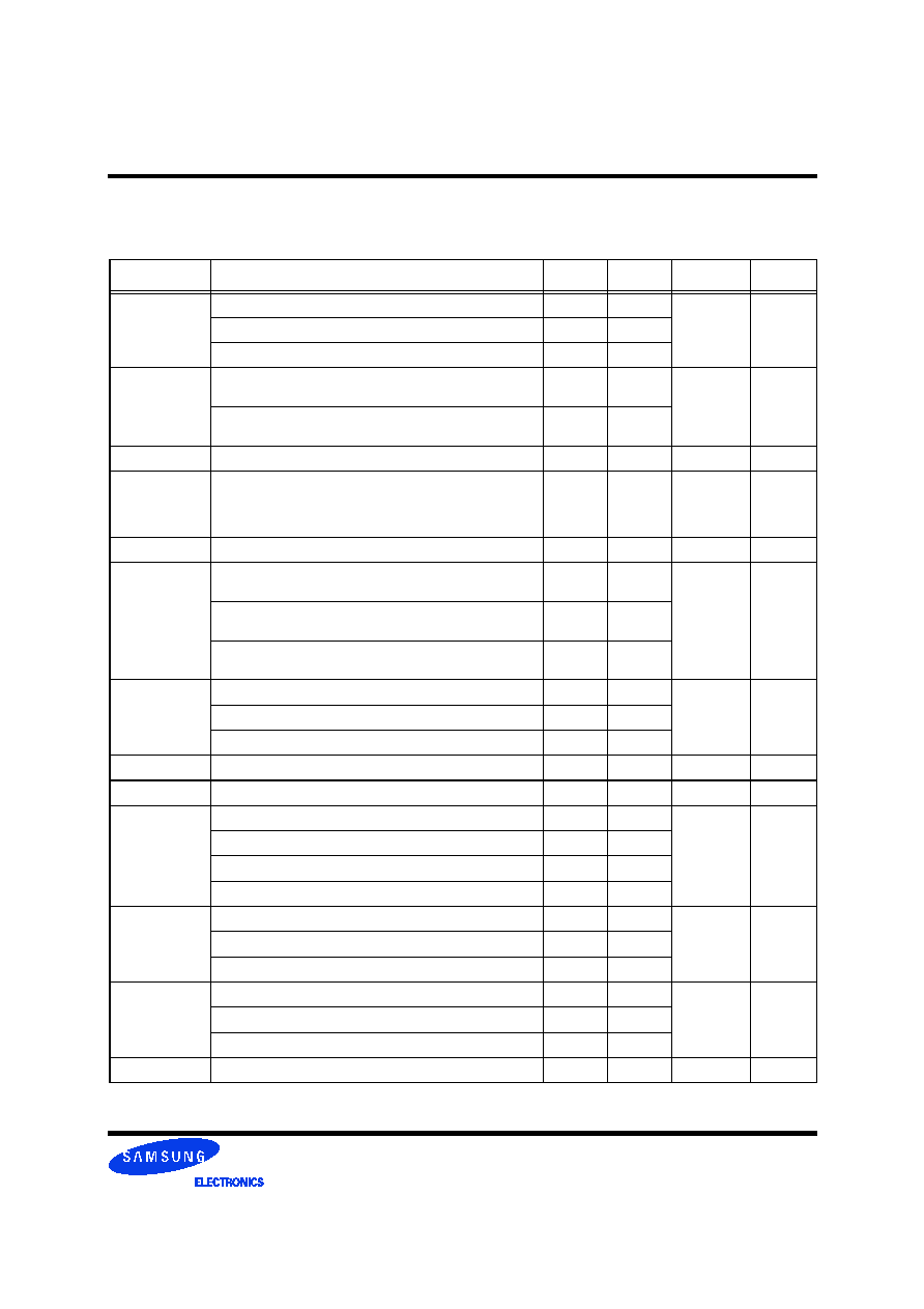
Key Timing Parameters/Part Numbers
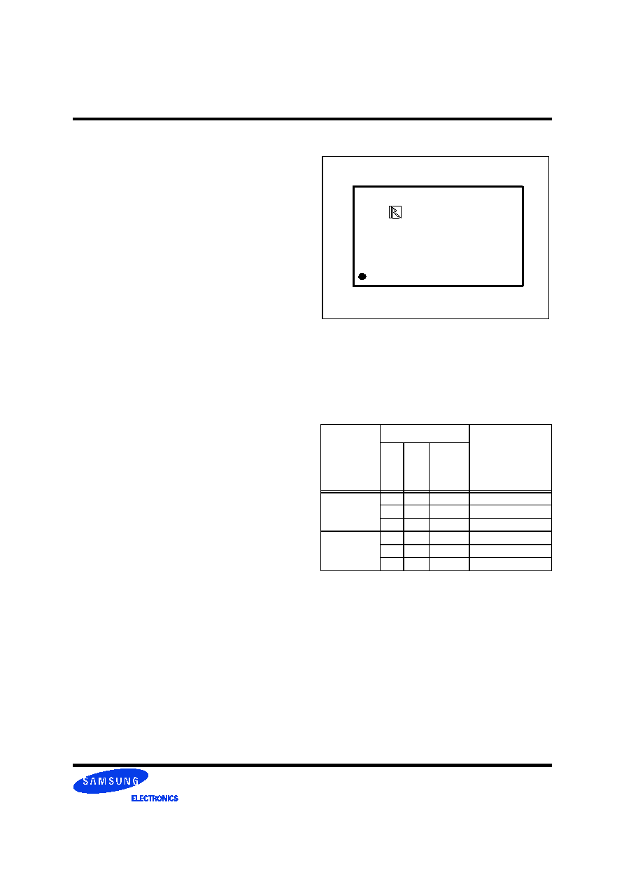
Figure 1: Direct RDRAM CSP Package
Organization
Speed
Part Number
Bin
I/O
Freq.
MHz
t
RAC
(Row
Access
Time) ns
1Mx18x32s
a
a.
"
32s
"
- 32 banks which use a
"
split
"
bank architecture.
-CN1
1200
32
K4R761869A-F
b
C
c
N1
b.
"
F
"
- WBGA package, "G"- WBGA lead free package.
c.
"
C
"
- RDRAM core uses normal power self refresh.
-CT9
1066
32P
K4R761869A-FCT9
-CM8
800
40
K4R761869A-FCM8
1Mx18x32s
-CN1
1200
32
K4R761869A-GCN1
-CT9
1066
32P
K4R761869A-GCT9
-CM8
800
40
K4R761869A-GCM8
K4R761869A-
x
Cxx
SAMSUNG 320
K4R761869A-
Cxx
SAMSUNG 320
K4R761869A-
Cxx
SAMSUNG 320
K4R761869A-
x
Cxx
SAMSUNG 320
K4R761869A-
Cxx
SAMSUNG 320
K4R761869A-
Cxx
SAMSUNG 320
Direct RDRAM
TM
Page 2
Version 1.41 Jan. 2004
K4R761869A
COL
ROW
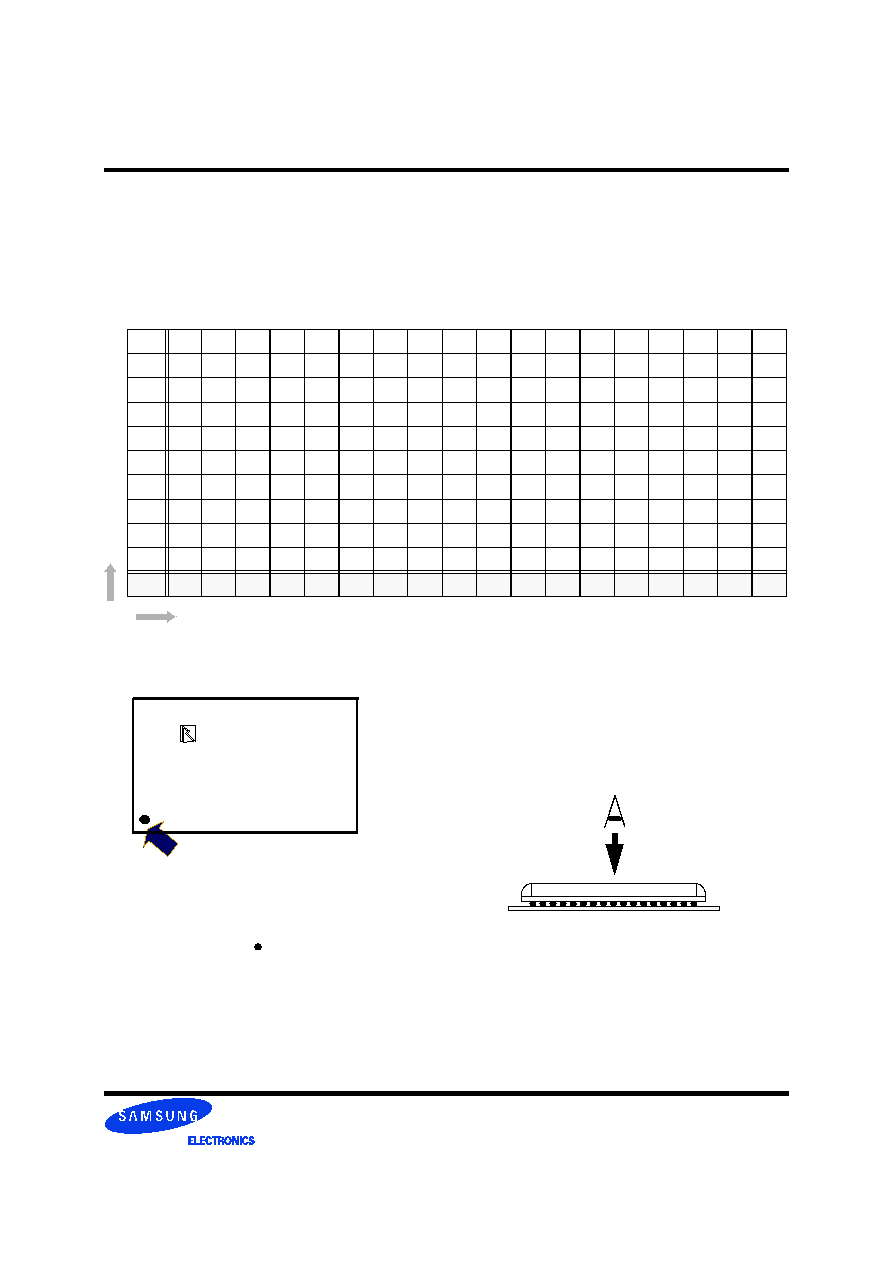
Pinouts and Definitions
Center-Bonded Devices
These tables shows the pin assignments of the center-bonded
RDRAM package. The mechanical dimensions of this
package are shown in a later section. Refer to Section
"
Center-Bonded WBGA Package
"
on page 18. Note - pin #1
is at the A1 position.
Table 1: Center-Bonded Device (top view)
10
V
DD
GND
V
DD
GND
V
DD
V
DD
V
DD
V
DD
GND
V
DD
9
8
GND
V
DD
CMD
V
DD
GND
GNDa
GNDa
V
DD
V
DD
GND
GND
V
DD
V
DD
GND
GND
V
CMOS
V
DD
GND
7
V
DD
DQA8
DQA7
DQA5
DQA3
DQA1
CTMN
CTM
RQ7
RQ5
RQ3
RQ1
DQB1
DQB3
DQB5
DQB7
DQB8
V
DD
6
5
4
GND
GND
DQA6
DQA4
DQA2
DQA0
CFM
CFMN
RQ6
RQ4
RQ2
RQ0
DQB0
DQB2
DQB4
DQB6
GND
GND
3
V
DD
GND
SCK
V
CMOS
GND
V
DD
GND
V
DDa
V
REF
GND
V
DD
GND
GND
V
DD
SIO0
SIO1
GND
V
DD
2
1
V
DD
GND
GND
V
DD
GND
GND
GND
GND
GND
V
DD
A
B
C
D
E
F
G
H
J
K
L
M
N
P
R
S
T
U
Chip
Top View
The pin #1(ROW 1, COL A) is located at the
A1 position on the top side and the A1 position
is marked by the marker
"
"
.
K4R761869A-
x
Cxx
SAMSUNG 320
K4R761869A-
x
Cxx
SAMSUNG 320
Direct RDRAM
TM
Page 3
K4R761869A
Version 1.41 Jan. 2004
Table 2: Pin Description
Signal
I/O
Type
# Pins
center
Description
SIO1,SIO0
I/O
CMOS
a
2
Serial input/output. Pins for reading from and writing to the control regis-
ters using a serial access protocol. Also used for power management.
CMD
I
CMOS
a
1
Command input. Pins used in conjunction with SIO0 and SIO1 for reading
from and writing to the control registers. Also used for power manage-
ment.
SCK
I
CMOS
a
1
Serial clock input. Clock source used for reading from and writing to the
control registers
V
DD
24
Supply voltage for the RDRAM core and interface logic.
V
DDa
1
Supply voltage for the RDRAM analog circuitry.
V
CMOS
2
Supply voltage for CMOS input/output pins.
GND
28
Ground reference for RDRAM core and interface.
GNDa
2
Ground reference for RDRAM analog circuitry.
DQA8..DQA0
I/O
RSL
b
9
Data byte A. Nine pins which carry a byte of read or write data between
the Channel and the RDRAM device. DQA8 is not used (no connection)
by RDRAM device with a x16 organization.
CFM
I
RSL
b
1
Clock from master. Interface clock used for receiving RSL signals from
the Channel. Positive polarity.
CFMN
I
RSL
b
1
Clock from master. Interface clock used for receiving RSL signals from
the Channel. Negative polarity
V
REF
1
Logic threshold reference voltage for RSL signals
CTMN
I
RSL
b
1
Clock to master. Interface clock used for transmitting RSL signals to the
Channel. Negative polarity.
CTM
I
RSL
b
1
Clock to master. Interface clock used for transmitting RSL signals to the
Channel. Positive polarity.
RQ7..RQ5 or
ROW2..ROW0
I
RSL
b
3
Row access control. Three pins containing control and address informa-
tion for row accesses.
RQ4..RQ0 or
COL4..COL0
I
RSL
b
5
Column access control. Five pins containing control and address informa-
tion for column accesses.
DQB8..
DQB0
I/O
RSL
b
9
Data byte B. Nine pins which carry a byte of read or write data between
the Channel and the RDRAM device. DQB8 is not used (no connection)
by RDRAM device with a x16 organization.
Total pin count per package
92
a. All CMOS signals are high-true; a high voltage is a logic one and a low voltage is logic zero.
b. All RSL signals are low-true; a low voltage is a logic one and a high voltage is logic zero.
Direct RDRAM
TM
Page 4
Version 1.41 Jan. 2004
K4R761869A
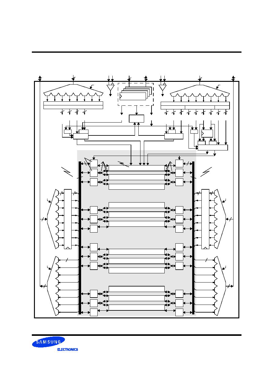
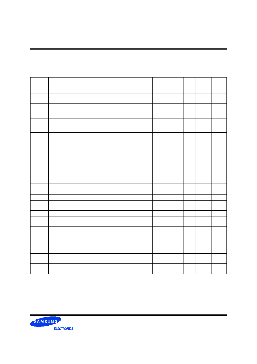
Figure 2: 576Mbit (1M x18 x32s) RDRAM Device Block Diagram
Bank 31
DQA8..DQA0
1:8 De
mux
8:
1 M
u
x
W
r
i
t
e
B
u
ffer
1:8
D
e
mux
W
r
ite Buffer
8:
1
M
u
x
Bank 30
Bank 29
Bank 18
Bank 17
Bank 16
Bank 15
Bank 14
Bank 13
Bank 1
Bank 0
SAmp
1/2
DQB8..DQB0
9
1:8 Demux
1:8 Demux
Packet Decode
9
5
3
ROW2..ROW0
COL4..COL0
CTM CTMN
CFM CFMN
2
SCK,CMD
RCLK
TCLK
Control Registers
DC
COP
C
BC
MA
MB
DX
XOP
BX
DR
R
ROP
BR
8
8
7
5
5
5
5
5
6
10
5
5
11
AV
M
S
Write
Buffer
Match
Match
Mux
Match
DEVID
1024x128x144
Internal DQB Data Path
Column Decode & Mask
72
9
9
72
9
DM
REFR
Row Decode
Mux
ACT
RD, WR
Power Modes
DRAM Core
Mux
XOP Decode
PREX
PREC
9
9
9
9
72
9
9
9
PRER
COLX
COLC
COLM
2
SIO0,SIO1
Sense Amp
Internal DQA Data Path
Packet Decode
ROWA
ROWR
RCLK
RCLK
RC
LK
TC
LK
RC
LK
TC
LK
RQ7..RQ5 or
RQ4..RQ0 or
SAmp
0/1
SAmp
0
SA
mp
14/15
SAmp
15
SAmp
13/14
SAmp
16/17
SAmp
17/18
SAmp
16
SAmp
29/30
SAmp
30/31
SAmp
31
64x72
SAmp
1/2
72
SAmp
0/1
SAmp
0
SAm
p
14/15
SAmp
15
SAmp
13
/
1
4
SA
mp
16/17
SAmp
17/18
SAmp
16
SAmp
29/30
SAmp
30/31
SAmp
31
64x72
64x72
Bank 2
���
���
���
���
��
�
��
�

Direct RDRAM
TM
Page 5
K4R761869A
Version 1.41 Jan. 2004
General Description
Figure 2 is a block diagram of the 576Mbit RDRAM device.
It consists of two major blocks: a
"
core
"
block built from
banks and sense amps similar to those found in other types
of DRAM, and a Direct Rambus
TM
interface block which
permits an external controller to access this core at up to
2.4GB/s.
Control Registers:
The CMD, SCK, SIO0 and SIO1
pins appear in the upper center of Figure 2. They are used to
write and read a block of control registers. These registers
supply the RDRAM configuration information to a
controller and they select the operating modes of the device.
The REFR value is used for tracking the last refreshed row.
Most importantly, the five bit DEVID specifies the device
address of the RDRAM device on the Channel.
Clocking:
The CTM and CTMN pins (Clock-To-Master)
generate TCLK (Transmit Clock), the internal clock used to
transmit read data. The CFM and CFMN pins (Clock-From-
Master) generate RCLK (Receive Clock), the internal clock
signal used to receive write data and to receive the ROW and
COL pins.
DQA,DQB Pins:
These 18 pins carry read (Q) and write
(D) data across the Channel. They are multiplexed/de-multi-
plexed from/to two 72-bit data paths (running at one-eighth
the data frequency) inside the RDRAM device.
Banks:
The 64Mbyte core of the RDRAM device is
divided into thirty two 2Mbyte banks, each organized as
1024 rows, with each row containing 128 dualocts, and each
dualoct containing 18 bytes. A dualoct is the smallest unit of
data that can be addressed.
Sense Amps:
The RDRAM device contains 34 sense
amps. Each sense amp consists of 1kbyte of fast storage (512
bytes for DQA and 512 bytes for DQB) and can hold one-
half of one row of one bank of the RDRAM device. The
sense amp may hold any of the 1024 half-rows of an associ-
ated bank. However, each sense amp is shared between two
adjacent banks of the RDRAM device (except for sense
amps 0, 15, 16, and 31). This introduces the restriction that
adjacent banks may not be simultaneously accessed.
RQ Pins:
These pins carry control and address informa-
tion. They are broken into two groups. RQ7..RQ5 are also
called ROW2..ROW0, and are used primarily for controlling
row accesses. RQ4..RQ0 are also called COL4..COL0, and
are used primarily for controlling column accesses.
ROW Pins:
The principle use of these three pins is to
manage the transfer of data between the banks and the sense
amps of the RDRAM device. These pins are de-multiplexed
into a 24-bit ROWA (row-activate) or ROWR (row-opera-
tion) packet.
COL Pins:
The principle use of these five pins is to
manage the transfer of data between the DQA/DQB pins and
the sense amps of the RDRAM device. These pins are de-
multiplexed into a 23-bit COLC (column-operation) packet
and either a 17-bit COLM (mask) packet or a 17-bit COLX
(extended-operation) packet.
ACT Command:
An ACT (activate) command from an
ROWA packet causes one of the 1024 rows of the selected
bank to be loaded to its associated sense amps (two 512
bytes sense amps for DQA and two for DQB).
PRER Command:
A PRER (precharge) command from
an ROWR packet causes the selected bank to release its two
associated sense amps, permitting a different row in that
bank to be activated, or permitting adjacent banks to be acti-
vated.
RD Command:
The RD (read) command causes one of
the 128 dualocts of one of the sense amps to be transmitted
on the DQA/DQB pins of the Channel.
WR Command:
The WR (write) command causes a
dualoct received from the DQA/DQB data pins of the
Channel to be loaded into the write buffer. There is also
space in the write buffer for the BC bank address and C
column address information. The data in the write buffer is
automatically retired (written with optional bytemask) to one
of the 128 dualocts of one of the sense amps during a subse-
quent COP command. A retire can take place during a RD,
WR, or NOCOP to another device, or during a WR or
NOCOP to the same device. The write buffer will not retire
during a RD to the same device. The write buffer reduces the
delay needed for the internal DQA/DQB data path turn-
around.
PREC Precharge:
The PREC, RDA and WRA
commands are similar to NOCOP, RD and WR, except that a
precharge operation is performed at the end of the column
operation. These commands provide a second mechanism
for performing precharge.
PREX Precharge:
After a RD command, or after a WR
command with no byte masking (M=0), a COLX packet may
be used to specify an extended operation (XOP). The most
important XOP command is PREX. This command provides
a third mechanism for performing precharge.
Direct RDRAM
TM
Page 6
Version 1.41 Jan. 2004
K4R761869A
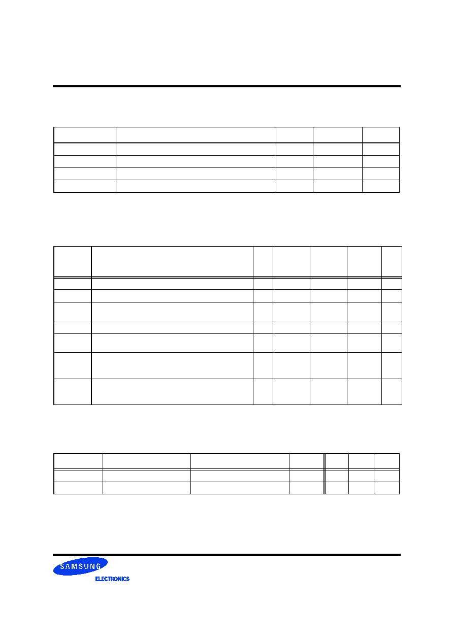
Packet Format
Figure 3 shows the formats of the ROWA and ROWR
packets on the ROW pins. Table 3 describes the fields which
comprise these packets. DR4T and DR4F bits are encoded to
contain both the DR4 device address bit and a framing bit
which allows the ROWA or ROWR packet to be recognized
by the RDRAM device.
The AV (ROWA/ROWR packet selection) bit distinguishes
between the two packet types. Both the ROWA and ROWR
packet provide a five bit device address and a five bit bank
address. An ROWA packet uses the remaining bits to specify
a nine bit row address, and the ROWR packet uses the
remaining bits for an eleven bit opcode field. Note the use of
the
"
RsvX
"
notation to reserve bits for future address field
extension.
Figure 3 also shows the formats of the COLC, COLM, and
COLX packets on the COL pins. Table 4 describes the fields
which comprise these packets.
The COLC packet uses the S (Start) bit for framing. A
COLM or COLX packet is aligned with this COLC packet,
and is also framed by the S bit.
The 23 bit COLC packet has a five bit device address, a five
bit bank address, a seven bit column address, and a four bit
opcode. The COLC packet specifies a read or write
command, as well as some power management commands.
The remaining 17 bits are interpreted as a COLM (M=1) or
COLX (M=0) packet. A COLM packet is used for a COLC
write command which needs bytemask control. The COLM
packet is associated with the COLC packet from at least t
RTR
earlier. A COLX packet may be used to specify an indepen-
dent precharge command. It contains a five bit device
address, a five bit bank address, and a five bit opcode. The
COLX packet may also be used to specify some house-
keeping and power management commands. The COLX
packet is framed within a COLC packet but is not otherwise
associated with any other packet.
Table 3: Field Description for ROWA Packet and ROWR Packet
Field
Description
DR4T,DR4F
Bits for framing (recognizing) a ROWA or ROWR packet. Also encodes highest device address bit.
DR3..DR0
Device address for ROWA or ROWR packet.
BR4..BR0
Bank address for ROWA or ROWR packet. RsvB denotes bits ignored by the
RDRAM device
.
AV
Selects between ROWA packet (AV=1) and ROWR packet (AV=0).
R9..R0
Row address for ROWA packet. RsvR denotes bits ignored by the
RDRAM device
.
ROP10..ROP0
Opcode field for ROWR packet. Specifies precharge, refresh, and power management functions.
Table 4: Field Description for COLC Packet, COLM Packet, and COLX Packet
Field
Description
S
Bit for framing (recognizing) a COLC packet, and indirectly for framing COLM and COLX packets.
DC4..DC0
Device address for COLC packet.
BC4..BC0
Bank address for COLC packet. RsvB denotes bits reserved for future extension (controller drives 0 ' s).
C6..C0
Column address for COLC packet. RsvC denotes bits ignored by the
RDRAM device
02.
COP3..COP0
Opcode field for COLC packet. Specifies read, write, precharge, and power management functions.
M
Selects between COLM packet (M=1) and COLX packet (M=0).
MA7..MA0
Bytemask write control bits. 1=write, 0=no-write. MA0 controls the earliest byte on DQA8..0.
MB7..MB0
Bytemask write control bits. 1=write, 0=no-write. MB0 controls the earliest byte on DQB8..0.
DX4..DX0
Device address for COLX packet.
BX4..BX0
Bank address for COLX packet. RsvB denotes bits reserved for future extension (controller drives 0' s).
XOP4..XOP0
Opcode field for COLX packet. Specifies precharge, I
OL
control, and power management functions.
Direct RDRAM
TM
Page 7
K4R761869A
Version 1.41 Jan. 2004
Figure 3: Packet Formats
CTM/CFM
COL4
COL3
COL2
COL1
COL0
T
8
T
9
T
10
T
11
T
12
T
13
T
14
T
15
T
8
T
9
T
10
T
11
T
0
T
1
T
2
T
3
T
0
T
1
T
2
T
3
S=1
a
MA7 MA5 MA3 MA1
M=1 MA6 MA4 MA2 MA0
MB7 MB4 MB1
MB6 MB3 MB0
MB5 MB2
R2
CTM/CFM
ROW2
DR4T DR2 BR0 BR3 RsvR R8
R5
ROW1
DR4F DR1 BR1 BR4
R9
R7
R4
R1
ROW0
DR3 DR0 BR2 RsvB AV=1 R6
R3
R0
ACT a0
PREX d0
MSK (b1)
PRER c0
WR b1
C4
CTM/CFM
COL4
DC4 S=1
C6
COL3
DC3
C5
C3
COL2
DC2 COP1
RsvB BC2
C2
DC1 COP0
BC4 BC1
C1
DC0 COP2
COP3 BC3 BC0
C0
COL1
COL0
CTM/CFM
ROW2
ROW1
ROW0
CTM/CFM
COL4
COL3
COL2
COL1
COL0
ROP2
DR4T DR2 BR0 BR3
ROP10
ROP8 ROP5
DR4F DR1 BR1 BR4 ROP9 ROP7 ROP4 ROP1
DR3 DR0 BR2 RsvB AV=0 ROP6 ROP3 ROP0
S=1
b
DX4 XOP4 RsvB BX1
M=0 DX3 XOP3 BX4 BX0
DX2 XOP2 BX3
DX1 XOP1 BX2
DX0 XOP0
T
0
T
4
T
8
T
12
T
1
T
5
T
9
T
13
T
2
T
6
T
10
T
14
T
3
T
7
T
11
T
15
ROWA Packet
COLM Packet
COLC Packet
COLX Packet
ROWR Packet
CTM/CFM
DQA8..0
DQB8..0
COL4
..COL0
ROW2
..ROW0
t
PACKET
a
The COLM is associated with a
previous COLC, and is aligned
with the present COLC, indicated
by the Start bit (S=1) position.
b
The COLX is aligned
with the present COLC,
indicated by the Start
bit (S=1) position.
Direct RDRAM
TM
Page 8
Version 1.41 Jan. 2004
K4R761869A
Field Encoding Summary
Table 5 shows how the six device address bits are decoded
for the ROWA and ROWR packets. The DR4T and DR4F
encoding merges a fifth device bit with a framing bit. When
neither bit is asserted, the device is not selected. Note that a
broadcast operation is indicated when both bits are set.
Broadcast operation would typically be used for refresh and
power management commands. If the device is selected, the
DM (DeviceMatch) signal is asserted and an ACT or ROP
command is performed.
Table 6 shows the encodings of the remaining fields of the
ROWA and ROWR packets. An ROWA packet is specified
by asserting the AV bit. This causes the specified row of the
specified bank of this device to be loaded into the associated
sense amps.
An ROWR packet is specified when AV is not asserted. An
11 bit opcode field encodes a command for one of the banks
of this device. The PRER command causes a bank and its
two associated sense amps to precharge, so another row or
an adjacent bank may be activated. The REFA (refresh-acti-
vate) command is similar to the ACT command, except the
row address comes from an internal register REFR, and
REFR is incremented at the largest bank address. The REFP
(refresh-precharge) command is identical to a PRER
command.
The NAPR, NAPRC, PDNR, ATTN, and RLXR commands
are used for managing the power dissipation of the RDRAM
device and are described in more detail in
"
Power State
Management
"
on page 50. The TCEN and TCAL commands
are used to adjust the output driver slew rate and they are
described in more detail in
"
Current and Temperature
Control
"
on page 56.
Table 5: Device Field Encodings for ROWA Packet and ROWR Packet
DR4T
DR4F
Device Selection
Device Match signal (DM)
1
1
All devices (broadcast)
DM is set to 1
0
1
One device selected
DM is set to 1 if {DEVID4..DEVID0} == {0,DR3..DR0} else DM is set to 0
1
0
One device selected
DM is set to 1 if {DEVID4..DEVID0} == {1,DR3..DR0} else DM is set to 0
0
0
No packet present
DM is set to 0
Table 6: ROWA Packet and ROWR Packet Field Encodings
DM
a
AV
ROP10..ROP0 Field
Name
Command Description
10 9
8
7
6
5
4
3
2:0
0
-
-
-
-
-
-
-
-
-
---
-
No operation.
1
1
Row address
ACT
Activate row R9..R0 of bank BR4..BR0 of device and move device to ATTN
b
.
1
0
1
1
0
0
0
x
c
x
x
000
PRER
Precharge bank BR4..BR0 of this device.
1
0
0
0
0
1
1
0
0
x
000
REFA
Refresh (activate) row REFR9..REFR0 of bank BR4..BR0 of device.
Increment REFR if BR4..BR0 = 11111 (see Figure 52).
1
0
1
0
1
0
1
0
0
x
000
REFP
Precharge bank BR4..BR0 of this device after REFA (see Figure 52).
1
0
x
x
0
0
0
0
1
x
000
PDNR
Move this device into the powerdown (PDN) power state (see Figure 49).
1
0
x
x
0
0
0
1
0
x
000
NAPR
Move this device into the nap (NAP) power state (see Figure 49).
1
0
x
x
0
0
0
1
1
x
000
NAPRC
Move this device into the nap (NAP) power state conditionally
1
0
x
x
x
x
x
x
x
0
000
ATTN
b
Move this device into the attention (ATTN) power state (see Figure 47).
1
0
x
x
x
x
x
x
x
1
000
RLXR
Move this device into the standby (STBY) power state (see Figure 48).
1
0
0
0
0
0
0
0
0
x
001
TCAL
Temperature calibrate this device (see Figure 55).
1
0
0
0
0
0
0
0
0
x
010
TCEN
Temperature calibrate/enable this device (see Figure 55).
1
0
0
0
0
0
0
0
0
0
000
NOROP
No operation.
a. The DM (Device Match signal) value is determined by the DR4T,DR4F, DR3..DR0 field of the ROWA and ROWR packets. See Table 5.
b. The ATTN command does not cause a RLX-to-ATTN transition for a broadcast operation (DR4T/DR4F=1/1).
c. An
"
x
"
entry indicates which commands may be combined. For instance, the three commands PRER/NAPRC/RLXR may be specified in one ROP value (011000111000).
Direct RDRAM
TM
Page 9
K4R761869A
Version 1.41 Jan. 2004
Table 7 shows the COP field encoding. The device must be
in the ATTN power state in order to receive COLC packets.
The COLC packet is used primarily to specify RD (read) and
WR (write) commands. Retire operations (moving data from
the write buffer to a sense amp) happen automatically. See
Figure 18 for a more detailed description.
The COLC packet can also specify a PREC command,
which precharges a bank and its associated sense amps. The
RDA/WRA commands are equivalent to combining RD/WR
with a PREC. RLXC (relax) performs a power mode transi-
tion. See
"
Power State Management
"
on page 50.
Table 8 shows the COLM and COLX field encodings. The
M bit is asserted to specify a COLM packet with two 8 bit
bytemask fields MA and MB. If the M bit is not asserted, an
COLX is specified. It has device and bank address fields,
and an opcode field. The primary use of the COLX packet is
to permit an independent PREX (precharge) command to be
specified without consuming control bandwidth on the ROW
pins. It is also used for the CAL(calibrate) and SAM (sam-
ple) current control commands (see
"
Current and Tempera-
ture Control
"
on page 56), and for the RLXX power mode
command (see
"
Power State Management
"
on page 50).
Table 7: COLC Packet Field Encodings
S
DC4.. DC0
(select device)
a
COP3..0
Name
Command Description
0
----
-----
-
No operation.
1
/= (DEVID4 ..0)
-----
-
Retire write buffer of this device.
1
== (DEVID4 ..0)
x000
b
NOCOP
Retire write buffer of this device.
1
== (DEVID4 ..0)
x001
WR
Retire write buffer of this device, then write column C6..C0 of bank BC4..BC0 to write buffer.
1
== (DEVID4 ..0)
x010
RSRV
Reserved, no operation.
1
== (DEVID4 ..0)
x011
RD
Read column C6..C0 of bank BC4..BC0 of this device.
1
== (DEVID4 ..0)
x100
PREC
Retire write buffer of this device, then precharge bank BC4..BC0 (see Figure 15).
1
== (DEVID4 ..0)
x101
WRA
Same as WR, but precharge bank BC4..BC0 after write buffer (with new data) is retired.
1
== (DEVID4 ..0)
x110
RSRV
Reserved, no operation.
1
== (DEVID4 ..0)
x111
RDA
Same as RD, but precharge bank BC4..BC0 afterward.
1
== (DEVID4 ..0)
1xxx
RLXC
Move this device into the standby (STBY) power state (see Figure 48).
a.
"
/=
"
means not equal,
"
==
"
means equal.
b. An
"
x
"
entry indicates which commands may be combined. For instance, the two commands WR/RLXC may be specified in one COP value (1001).
Table 8: COLM Packet and COLX Packet Field Encodings
M
DX4 .. DX0
(selects device)
XOP4..0
Name
Command Description
1
----
-
MSK
MB/MA bytemasks used by WR/WRA.
0
/= (DEVID4 ..0)
-
-
No operation.
0
== (DEVID4 ..0)
00000
NOXOP
No operation.
0
== (DEVID4 ..0)
1xxx0
a
PREX
Precharge bank BX3..BX0 of this device (see Figure 15).
0
== (DEVID4 ..0)
x10x0
CAL
Calibrate (drive) I
OL
current for this device (see Figure 54).
0
== (DEVID4 ..0)
x11x0
CAL/SAM
Calibrate (drive) and Sample ( update) I
OL
current for this device (see Figure 54).
0
== (DEVID4 ..0)
xxx10
RLXX
Move this device into the standby (STBY) power state (see Figure 48).
0
== (DEVID4 ..0)
xxxx1
RSRV
Reserved, no operation.
a. An
"
x
"
entry indicates which commands may be combined. For instance, the two commands PREX/RLXX may be specified in one XOP value (10010).

Direct RDRAM
TM
Page 10
Version 1.41 Jan. 2004
K4R761869A
Electrical Conditions
Table 9: Electrical Conditions
Symbol
Parameter and Conditions
Min
Max
Unit
T
J
Junction temperature under bias
-
100
�C
V
DD,
V
DDA
Supply voltage
2.50 - 0.13
2.50 + 0.13
V
V
DD,N,
V
DDA,N
Supply voltage droop (DC) during NAP interval (t
NLIMIT
)
-
2.0
%
v
DD,N,
v
DDA,N
Supply voltage ripple (AC) during NAP interval (t
NLIMIT
)
-2.0
2.0
%
V
CMOS
a
Supply voltage for CMOS pins (2.5V controllers)
Supply voltage for CMOS pins (1.8V controllers)
V
DD
1.80 - 0.1
V
DD
1.80 + 0.2
V
V
V
REF
Reference voltage
1.40 - 0.2
1.40 + 0.2
V
V
DIL
RSL data input - low voltage @ t
CYCLE
=1.667ns
V
REF
- 0.5
V
REF
- 0.15
V
RSL data input - low voltage @ t
CYCLE
=1.875ns
V
REF
- 0.5
V
REF
- 0.15
RSL data input - low voltage @ t
CYCLE
=2.50ns
V
REF
- 0.5
V
REF
- 0.2
V
DIH
RSL data input - high voltage
b
@ t
CYCLE
=1.667ns
V
REF
+ 0.15
V
REF
+ 0.5
RSL data input - high voltage
b
@ t
CYCLE
=1.875ns
V
REF
+ 0.15
V
REF
+ 0.5
V
RSL data input - high voltage
b
@ t
CYCLE
=2.50ns
V
REF
+ 0.2
V
REF
+ 0.5
R
DA
RSL data asymmetry : R
DA
= (V
DIH
- V
REF
) / (V
REF
- V
DIL
)
0.67
1.00
-
V
CM
RSL clock input - common mode V
CM
= (V
CIH
+V
CIL)
/2
1.3
1.8
V
V
CIS,CTM
RSL clock input swing: V
CIS
= V
CIH
- V
CIL
(CTM,CTMN pins).
0.35
1.00
V
V
CIS,CFM
RSL clock input swing: V
CIS
= V
CIH
- V
CIL
(CFM,CFMN pins).
0.225
1.00
V
V
IL,CMOS
CMOS input low voltage
- 0.3
c
V
CMOS
/2 - 0.25
V
V
IH,CMOS
CMOS input high voltage
V
CMOS
/2 + 0.25
V
CMOS
+0.3
d
V
a. V
CMOS
must remain on as long as V
DD
is applied and cannot be turned off.
b. V
DIH
is typically equal to V
TERM
(1.8V
�
0.1V) under DC conditions in a system.
c. Voltage undershoot is limited to -0.7V for a duration of less than 5ns.
d. Voltage overshoot is limited toV
CMOS
+0.7V for a duration of less than 5ns

Direct RDRAM
TM
Page 11
K4R761869A
Version 1.41 Jan. 2004
Electrical Characteristics
Table 10: Electrical Characteristics
Symbol
Parameter and Conditions
Min
Max
Unit
JC
Junction-to-Case thermal resistance
-
0.5
�C/Watt
I
REF
V
REF
current @ V
REF,MAX
-10
10
�A
I
OH
RSL output high current @ (0
V
OUT
V
DD
)
-10
10
�A
I
ALL
RSL I
OL
current @ t
CYCLE
= 1.667ns V
OL
= 0.9V, V
DD,MIN
, T
J,MAX
a
a. This measurement is made in manual current control mode; i.e. with all output device legs sinking current.
32.0
90.0
mA
RSL I
OL
current @ t
CYCLE
= 1.875ns V
OL
= 0.9V, V
DD,MIN
, T
J,MAX
a
32.0
90.0
RSL I
OL
current @ t
CYCLE
=2.50ns V
OL
= 0.9V, V
DD,MIN
, T
J,MAX
a
30.0
90.0
I
OL
RSL
I
OL
current resolution step
-
1.5
mA
r
OUT
Dynamic output impedance @ V
OL
= 0.9V
150
-
I
OL,NOM
RSL I
OL
current @ V
OL
= 1.0V
b,c
@ t
CYCLE
=1.667ns
b. This measurement is made in automatic current control mode after at least 64 current control calibration operations to a device and after CCA and
CCB are initialized to a value of 64. This value applies to all DQA and DQB pins.
c. This measurement is made in automatic current control mode in a 25
test system with V
TERM
= 1.714V and V
REF
= 1.357V and with the ASYMA
and ASYMB register fields set to 0.
27.1
30.1
mA
RSL I
OL
current @ V
OL
= 1.0V
b,c
@ t
CYCLE
=1.875ns
27.1
30.1
RSL I
OL
current @ V
OL
= 1.0V
b,c
@ t
CYCLE
=2.5ns
26.6
30.6
I
I,CMOS
CMOS input leakage current @ (0
V
I,CMOS
V
CMOS
)
-10.0
10.0
�A
V
OL,CMOS
CMOS output voltage @ I
OL,CMOS
= 1.0mA
-
0.3
V
V
OH,CMOS
CMOS output high voltage @ I
OH,CMOS
= -0.25mA
V
CMOS
-0.3
-
V
Direct RDRAM
TM
Page 12
Version 1.41 Jan. 2004
K4R761869A
Timing Conditions
Table 11: Timing Conditions
Symbol
Parameter
Min
Max
Unit
Figure(s)
t
CYCLE
CTM and CFM cycle times (-1200)
1.667
2.5
ns
Figure 56
CTM and CFM cycle times (-1066)
1.875
2.5
CTM and CFM cycle times (-800)
2.50
3.33
t
CR
, t
CF
CTM and CFM input rise and fall times. Use the minimum value of
these parameters during testing. (-1200)
0.2
0.45
ns
Figure 56
CTM and CFM input rise and fall times. Use the minimum value of
these parameters during testing. (-1066,-800)
0.2
0.5
t
CH
, t
CL
CTM and CFM high and low times
40%
60%
t
CYCLE
Figure 56
t
TR
CTM-CFM differential (MSE/MS=0/0)
CTM-CFM differential (MSE/MS=1/1)
a
CTM-CFM differential only for 1.875ns and 1.667ns (MSE/MS=1/0)
0.0
0.9
-0.1
1.0
1.0
0.1
t
CYCLE
Figure 43
Figure 56
t
DCW
Domain crossing window
-0.1
0.1
t
CYCLE
Figure 62
t
DR
, t
DF
DQA/DQB/ROW/COL input rise/fall times (20% to 80%). Use the
minimum value of these parameters during testing.@ t
CYCLE
=1.667ns
0.2
0.45
ns
Figure 57
DQA/DQB/ROW/COL input rise/fall times (20% to 80%). Use the
minimum value of these parameters during testing.@ t
CYCLE
=1.875ns
0.2
0.45
DQA/DQB/ROW/COL input rise/fall times (20% to 80%). Use the
minimum value of these parameters during testing.@ t
CYCLE
=2.50ns
0.2
0.65
t
S
, t
H
DQA/DQB/ROW/COL-to-CFM set/hold @ t
CYCLE
=1.667ns
0.140
b
-
ns
Figure 57
DQA/DQB/ROW/COL-to-CFM set/hold @ t
CYCLE
=1.875ns
0.160
b,c
-
DQA/DQB/ROW/COL-to-CFM set/hold @ t
CYCLE
=2.50ns
0.200
b.d
-
t
DR1,
t
DF1
SIO0, SIO1 input rise and fall times
-
5.0
ns
Figure 59
t
DR2,
t
DF2
CMD, SCK input rise and fall times
-
2.0
ns
Figure 59
t
CYCLE1
SCK cycle time - Serial control register transactions
1000
-
ns
Figure 59
SCK cycle time - Power transitions @ t
CYCLE
=1.667ns
7.5
-
SCK cycle time - Power transitions @ t
CYCLE
=1.875ns
7.5
-
SCK cycle time - Power transitions @ t
CYCLE
=2.50ns
10
-
t
CH1
, t
CL1
SCK high and low times @ t
CYCLE
=1.667ns
3.5
-
ns
Figure 59
SCK high and low times @ t
CYCLE
=1.875ns
3.5
-
SCK high and low times @ t
CYCLE
=2.50ns
4.25
-
t
S1
CMD setup time to SCK rising or falling edge
e
@ t
CYCLE
=1.667ns
1.0
-
ns
Figure 59
CMD setup time to SCK rising or falling edge
e
@ t
CYCLE
=1.875ns
1.0
-
CMD setup time to SCK rising or falling edge
e
@ t
CYCLE
=2.50ns
1.25
-
t
H1
CMD hold time to SCK rising or falling edge
e
1
-
ns
Figure 59

Direct RDRAM
TM
Page 13
K4R761869A
Version 1.41 Jan. 2004
t
S2
SIO0 setup time to SCK falling edge
40
-
ns
Figure 59
t
H2
SIO0 hold time to SCK falling edge
40
-
ns
Figure 59
t
S3
PDEV setup time on DQA5..0 to SCK rising edge.
0
-
ns
Figure 50
t
H3
PDEV hold time on DQA5..0 to SCK rising edge.
5.5
-
ns
Figure 60
t
S4
ROW2..0, COL4..0 setup time for quiet window
-1
-
t
CYCLE
Figure 50
t
H4
ROW2..0, COL4..0 hold time for quiet window
f
5
-
t
CYCLE
Figure 50
t
NPQ
Quiet on ROW/COL bits during NAP/PDN entry
4
-
t
CYCLE
Figure 49
t
READTOCC
Offset between read data and CC packets (same device)
12
-
t
CYCLE
Figure 54
t
CCSAMTOREAD
Offset between CC packet and read data (same device)
8
-
t
CYCLE
Figure 54
t
CE
CTM/CFM stable before NAP/PDN exit
2
-
t
CYCLE
Figure 50
t
CD
CTM/CFM stable after NAP/PDN entry
100
-
t
CYCLE
Figure 49
t
FRM
ROW packet to COL packet ATTN framing delay
7
-
t
CYCLE
Figure 48
t
NLIMIT
Maximum time in NAP mode
10.0
ms
Figure 47
t
REF
Refresh interval
32
ms
Figure 52
t
BURST
Interval after PDN or NAP (with self-refresh) exit in which all banks
of the RDRAM device must be refreshed at least once.
200
ms
Figure 53
t
CCTRL
Current control interval
34 t
CYCLE
100ms
ms/t
CYCLE
Figure 54
t
TEMP
Temperature control interval
100
ms
Figure 55
t
TCEN
TCE command to TCAL command
150
-
t
CYCLE
Figure 55
t
TCAL
TCAL command to quiet window
2
2
t
CYCLE
Figure 55
t
TCQUIET
Quiet window (no read data)
140
-
t
CYCLE
Figure 55
t
PAUSE
RDRAM device delay (no RSL operations allowed)
200.0
ms
page 38
a. MSE/MS are fields of the SKIP register. For this combination (skip override) the tDCW parameter range is effectively 0.0 to 0.0.
b.
t
S,MIN
and t
H,MIN
for other t
CYCLE
values can be interpolated between or extrapolated from the timings at the 2 specified t
CYCLE
values.
c. This parameter also applies to a-1200 part when operated with t
CYCLE
= 1.875ns
d. This parameter also applies to a-1200 or -1066 part when operated with t
CYCLE
= 2.50ns
e. With V
IL,CMOS
=0.5V
CMOS
-0.4V and V
IH,CMOS
=0.5V
CMOS
+0.4V
f. Effective hold becomes t
H4
'=t
H4
+[PDNXA�64�t
SCYCLE
+t
PDNXB,MAX
]-[PDNX�256�t
SCYCLE
] if [PDNX�256�t
SCYCLE
] < [PDNXA�64�t
SCYCLE
+t
PD-
NXB,MAX
]. See Figure 50
Table 11: Timing Conditions
Symbol
Parameter
Min
Max
Unit
Figure(s)
Direct RDRAM
TM
Page 14
K4R761869A
Version 1.41 Jan. 2004
Timing Characteristics
Table 12: Timing Characteristics
Symbol
Parameter
Min
Max
Unit
Figure(s)
t
Q
CTM-to-DQA/DQB output time @ t
CYCLE
=1.667ns
-0.170
a
a. t
Q,MIN
and t
Q,MAX
for other t
CYCLE
values can be interpolated between or extrapolated from the timings at the 3 specified t
CYCLE
values.
b. This parameter also applies to a-1200 part when operated with t
CYCLE
= 1.875ns
c. This parameter also applies to a-1200 or -1066 part when operated with t
CYCLE
= 2.50ns
+0.170
a
ns
Figure 58
CTM-to-DQA/DQB output time @ t
CYCLE
=1.875ns
-0.195
a,b
+0.195
a,b
CTM-to-DQA/DQB output time @ t
CYCLE
=2.5ns
-0.260
a,c
+0.260
a,c
t
QR
, t
QF
DQA/DQB output rise and fall times @ t
CYCLE
=1.667ns
0.2
0.32
ns
Figure 58
DQA/DQB output rise and fall times @ t
CYCLE
=1.875ns
0.2
0.32
DQA/DQB output rise and fall times @ t
CYCLE
=2.5ns
0.2
0.45
t
Q1
SCK(neg)-to-SIO0 delay @ C
LOAD,MAX
= 20pF (SD read data valid).
-
10
ns
Figure 61
t
HR
SCK(pos)-to-SIO0 delay @ C
LOAD,MAX
= 20pF (SD read data hold).
2
-
ns
Figure 61
t
QR1
, t
QF1
SIO
OUT
rise/fall @ C
LOAD,MAX
= 20pF
-
12
ns
Figure 61
t
PROP1
SIO0-to-SIO1 or SIO1-to-SIO0 delay @ C
LOAD,MAX
= 20pF
-
20
ns
Figure 61
t
NAPXA
NAP exit delay - phase A
-
50
ns
Figure 50
t
NAPXB
NAP exit delay - phase B
-
40
ns
Figure 50
t
PDNXA
PDN exit delay - phase A
-
4
�s
Figure 50
t
PDNXB
PDN exit delay - phase B
-
9000
t
CYCLE
Figure 50
t
AS
ATTN-to-STBY power state delay
-
1
t
CYCLE
Figure 48
t
SA
STBY-to-ATTN power state delay
-
0
t
CYCLE
Figure 48
t
ASN
ATTN/STBY-to-NAP power state delay
-
8
t
CYCLE
Figure 49
t
ASP
ATTN/STBY-to-PDN power state delay
-
8
t
CYCLE
Figure 49
Direct RDRAM
TM
Page 15
K4R761869A
Version 1.41 Jan. 2004
Timing Parameters
Table 13: Timing Parameter Summary
Parameter
Description
Min
-32
-1200
Min
-32P
-1066
Min
-40
-800
Max
Units
Figure(s)
t
RC
Row Cycle time of RDRAM banks -the interval between ROWA
packets with ACT commands to the same bank.
32
28
28
-
t
CYCLE
Figure 16
Figure 17
t
RAS
RAS-asserted time of RDRAM bank - the interval between ROWA
packet with ACT command and next ROWR packet with PRER
a
command to the same bank.
22
20
20
64
�s
b
t
CYCLE
Figure 16
Figure 17
t
RP
Row Precharge time of RDRAM banks - the interval between ROWR
packet with PRER
a
command and next ROWA packet with ACT
command to the same bank.
10
8
8
-
t
CYCLE
Figure 16
Figure 17
t
PP
Precharge-to-precharge time of RDRAM device - the interval
between successive ROWR packets with PRER
a
commands to any
banks of the same device.
8
8
8
-
t
CYCLE
Figure 13
t
RR
RAS-to-RAS time of RDRAM device - the interval between succes-
sive ROWA packets with ACT commands to any banks of the same
device.
8
8
8
-
t
CYCLE
Figure 14
t
RCD
RAS-to-CAS Delay - the interval from ROWA packet with ACT
command to COLC packet with RD or WR command). Note - the
RAS-to-CAS delay seen by the RDRAM core (t
RCD-C
) is equal to
t
RCD-C
= 1 + t
RCD
because of differences in the row and column paths
through the RDRAM interface.
9
9
7
-
t
CYCLE
Figure 16
Figure 17
t
CAC
CAS Access delay - the interval from RD command to Q read data.
The equation for t
CAC
is given in the TPARM register in Figure 40.
9
8
8
12
t
CYCLE
Figure 5
Figure 40
t
CWD
CAS Write Delay (interval from WR command to D write data.
6
6
6
6
t
CYCLE
Figure 5
t
CC
CAS-to-CAS time of RDRAM bank - the interval between successive
COLC commands).
4
4
4
-
t
CYCLE
Figure 16
Figure 17
t
PACKET
Length of ROWA, ROWR, COLC, COLM or COLX packet.
4
4
4
4
t
CYCLE
Figure 3
t
RTR
Interval from COLC packet with WR command to COLC packet
which causes retire, and to COLM packet with bytemask.
8
8
8
-
t
CYCLE
Figure 18
t
OFFP
The interval (offset) from COLC packet with RDA command, or
from COLC packet with retire command (after WRA automatic pre-
charge), or from COLC packet with PREC command, or from COLX
packet with PREX command to the equivalent ROWR packet with
PRER. The equation for t
OFFP
is given in the TPARM register in
Figure 40.
4
4
4
4
t
CYCLE
Figure 15
Figure 40
t
RDP
Interval from last COLC packet with RD command to ROWR packet
with PRER.
4
4
4
-
t
CYCLE
Figure 16
t
RTP
Interval from last COLC packet with automatic retire command to
ROWR packet with PRER.
4
4
4
-
t
CYCLE
Figure 17
a. Or equivalent PREC or PREX command. See Figure 15.
b. This is a constraint imposed by the core, and is therefore in units of
�s rather than t
CYCLE
.
Direct RDRAM
TM
Page 16
Version 1.41 Jan. 2004
K4R761869A
Absolute Maximum Ratings
Note*) Component : refer to T
J,
JC
Module : refre to T
PLATE, MAX
I
DD
- Supply Current Profile
Table 14: Absolute Maximum Ratings
Symbol
Parameter
Min
Max
Unit
V
I,ABS
Voltage applied to any RSL or CMOS pin with respect to Gnd
- 0.3
V
DD
+0.3
V
V
DD,ABS
, V
DDA,ABS
Voltage on VDD and VDDA with respect to Gnd
- 0.5
V
DD
+1.0
V
T
STORE
Storage temperature
- 50
100
�C
T
MIN
Minimum operation temperature
0
Note*
�C
Table 15: Supply Current Profile
I
DD
value
RDRAM Power State and Steady-State Transaction Rates
a
Min
Max
(1200MHz
, -32)
Max
(1066MHz
, -32P)
Max
(800MHz,
-40)
Unit
I
DD,PDN
Device in PDN, self-refresh enabled and INIT.LSR=0.
-
9000
9000
9000
�A
I
DD,NAP
Device in NAP.
-
4
4
4
mA
I
DD,STBY
Device in STBY. This is the average for a device in STBY with (1) no
packets on the Channel, and (2) with packets sent to other devices.
-
110
110
95
mA
I
DD,REFRESH
Device in STBY and refreshing rows at the t
REF,MAX
period.
-
110
110
95
mA
I
DD,ATTN
Device in ATTN. This is the average for a device in ATTN with (1) no
packets on the Channel, and (2) with packets sent to other devices.
-
165
160
135
mA
I
DD,ATTN-W
Device in ATTN. ACT command every 8�t
CYCLE
, PRE command
every 8�t
CYCLE
, WR command every 4
�
t
CYCLE
, and data is
1100..1100
-
980(x18)
b
930(x18)
730(x18)
mA
I
DD,ATTN-R
Device in ATTN. ACT command every 8�t
CYCLE
, PRE command
every 8
�
t
CYCLE
, RD command every 4
�
t
CYCLE
, and data is
1111..1111
c
-
960(x18)
900(x18)
720(x18)
mA
a. CMOS interface consumes power in all power states.
b. x18 RDRAM device data width.
c. This does not include the I
OL
sink current. The RDRAM device dissipates I
OL
�
V
OL
in each output driver when a logic one is driven.
Table 16: Supply Current at Initialization
Symbol
Parameter
Allowed Range of t
CYCLE
V
DD
Min
Max
Unit
I
DD,PWRUP,D
I
DD
from power -on to SETR
1.667ns to 2.5ns
V
DD,MIN
-
200
a
mA
I
DD,SETR,D
I
DD
from SETR to CLRR
1.667ns to 2.5ns
V
DD,MIN
-
332
mA
a. The supply current will be 150mA when tCYCLE is in the range 15ns to 1000ns.

Direct RDRAM
TM
Page 17
K4R761869A
Version 1.41 Jan. 2004
Capacitance and Inductance
Table 17: RSL Pin Parasitics
Symbol
Parameter and Conditions - RSL pins
Min
Max
Unit
Figure
L
I
RSL effective input inductance
@ t
CYCLE
=1.667ns
-
3.5
nH
Figure 63
RSL effective input inductance
@ t
CYCLE
=1.875ns
-
3.5
RSL effective input inductance
@ t
CYCLE
=2.5ns
-
4.0
L
12
Mutual inductance between any DQA or DQB RSL signals.
-
0.2
nH
Figure 63
Mutual inductance between any ROW or COL RSL signals.
-
0.6
nH
L
I
Difference in L
I
value between any RSL pins of a single device.
-
1.8
nH
Figure 63
C
I
RSL effective input capacitance
a
@ t
CYCLE
=1.667ns
2.0
2.3
pF
Figure 63
RSL effective input capacitance
a
@ t
CYCLE
=1.875ns
2.0
2.3
RSL effective input capacitance
a
@ t
CYCLE
=2.5ns
2.0
2.4
C
12
Mutual capacitance between any RSL signals.
-
0.1
pF
Figure 63
C
I
Difference in C
I
value between average of {CTM, CTMN,
CFM, CFMN} and any RSL pins of a single device.
-
0.06
pF
Figure 63
R
I
RSL effective input resistance
@ t
CYCLE
=1.667ns
4
10
Figure 63
RSL effective input resistance
@ t
CYCLE
=1.875ns
4
10
RSL effective input resistance
@ t
CYCLE
=2.5ns
4
15
a. This value is a combination of the device IO circuitry and package capacitances
Table 18: CMOS Pin Parasitics
Symbol
Parameter and Conditions - CMOS pins
Min
Max
Unit
Figure
L
I ,CMOS
CMOS effective input inductance
-
8.0
nH
Figure 63
C
I ,CMOS
CMOS effective input capacitance (SCK,CMD)
a
1.7
2.1
pF
C
I ,CMOS,SIO
CMOS effective input capacitance (SIO1, SIO0)
a
-
7.0
pF
a. This value is a combination of the device IO circuitry and package capacitances.
Direct RDRAM
TM
Page 18
Version 1.41 Jan. 2004
K4R761869A
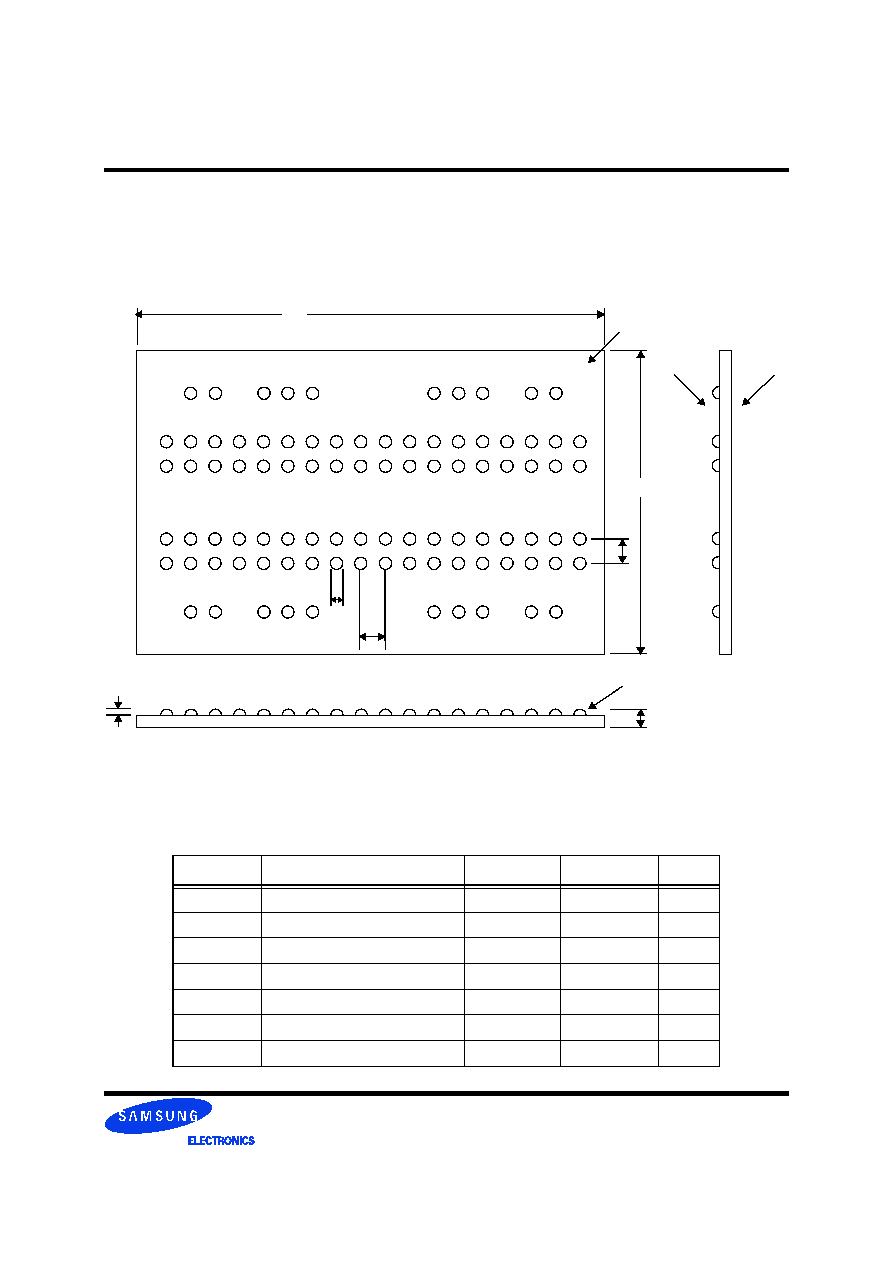
Center-Bonded WBGA Package
(92balls)
Figure 4 shows the form and dimensions of the recom-
mended package for the 92balls center-bonded WBGA
device class.
Figure 4: Center-Bonded WBGA Package
Table 19 lists the numerical values corresponding to dimen-
sions shown in Figure 4.
A
B C D
E
F
G H
J
1
2
3
4
5
6
7
D
A
e1
d
E
E1
8
e2
Top
Bottom
Bottom
9
10
K
L M N
P
R
S
T U
Bottom
Table 19 : Center-Bonded WBGA Package Dimensions
Symbol
Parameter
Min.
Max
.
Unit
e1
Ball pitch (x-axis)
0.80
0.80
mm
e2
Ball pitch (y-axis)
0.80
0.80
mm
A
Package body length
13.3
13.5
mm
D
Package body width
15.0
15.2
mm
E
Package total thickness
0.90
1.00
mm
E1
Ball height
0.30
0.40
mm
d
Ball diameter
0.40
0.50
mm