K4S161622H
CMOS SDRAM
Rev 0.3 October '03
Target
Revision History
Revision 0.0 (May, 2003)
∑ Target spec release
Revision 0.1 (October, 2003)
∑ Modified tRDL from 1CLK to 2CLK.
Revision 0.2 (October, 2003)
∑ Deleted AC parameter notes 5.
Revision 0.3 (October, 2003)
∑ Modified tRDL & deleted speed 200MHz.
K4S161622H
CMOS SDRAM
Rev 0.3 October '03
Target
The K4S161622H is 16,777,216 bits synchronous high data
rate Dynamic RAM organized as 2 x 524,288 words by 16 bits,
fabricated with SAMSUNG
s high performance CMOS technol-
ogy. Synchronous design allows precise cycle control with the
use of system clock I/O transactions are possible on every clock
cycle. Range of operating frequencies, programmable burst
length and programmable latencies allow the same device to be
useful for a variety of high bandwidth, high performance mem-
ory system applications.
∑
3.3V power supply
∑ LVTTL compatible with multiplexed address
∑ Dual banks operation
∑ MRS cycle with address key programs
-. CAS Latency ( 2 & 3)
-. Burst Length (1, 2, 4, 8 & full page)
-. Burst Type (Sequential & Interleave)
∑ All inputs are sampled at the positive going edge of the system
clock
∑
Burst Read Single-bit Write operation
∑
DQM for masking
∑
Auto & self refresh
∑ 15.6us refresh duty cycle (2K/32ms)
GENERAL DESCRIPTION
FEATURES
512K x 16Bit x 2 Banks Synchronous DRAM
ORDERING INFORMATION
Part NO.
MAX Freq.
Interface Package
K4S161622H-TC55
183MHz
LVTTL
50
TSOP(II)
K4S161622H-TC60
166MHz
K4S161622H-TC70
143MHz
K4S161622H-TC80
125MHz
K4S161622H-TC10
100MHz
11
.
7
6
±
0.2
0
0.46
3
±
0.00
8
0.002
0.05
MIN
0.008
0.21
±
0.002
±
0.05
0
.
020
0.
50
(
)
0.005
-0.001
+0.003
0.125
-0.035
+0.075
0
.
400
10
.
1
6
0.45
~0.7
5
0.0
18~
0.03
0
0.010
0.25
TYP
0~8
∞
C
#50
#26
#1
#25
0.004
0.10
MAX
0.028
0.71
( )
0.012
0.30
0.0315
0.80
0.047
1.20
MAX
0.039
1.00
±
0.004
±
0.10
0.891
22.62
MAX
0.875
22.22
±
0.004
±
0.10
+0.10
-0.05
+
0.004
-0.002
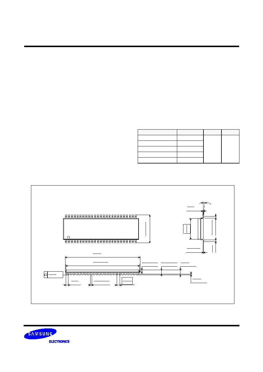
50Pin TSOP(II) Package Dimension
Package Physical Dimension

K4S161622H
CMOS SDRAM
Rev 0.3 October '03
Target
V
DD
DQ0
DQ1
V
SSQ
DQ2
DQ3
V
DDQ
DQ4
DQ5
V
SSQ
DQ6
DQ7
V
DDQ
LDQM
WE
CAS
RAS
CS
BA
A10/AP
A0
A1
A2
A3
V
DD
1
2
3
4
5
6
7
8
9
10
11
12
13
14
15
16
17
18
19
20
21
22
23
24
25
50
49
48
47
46
45
44
43
42
41
40
39
38
37
36
35
34
33
32
31
30
29
28
27
26
PIN CONFIGURATION (TOP VIEW)
V
SS
DQ15
DQ14
V
SSQ
DQ13
DQ12
V
DDQ
DQ11
DQ10
V
SSQ
DQ9
DQ8
V
DDQ
N.C/RFU
UDQM
CLK
CKE
N.C
A9
A8
A7
A6
A5
A4
V
SS
50PIN TSOP (II)
(400mil x 825mil)
(0.8 mm PIN PITCH)
PIN FUNCTION DESCRIPTION
Pin
Name
Input Function
CLK
System Clock
Active on the positive going edge to sample all inputs.
CS
Chip Select
Disables or enables device operation by masking or enabling all inputs except
CLK, CKE and L(U)DQM
CKE
Clock Enable
Masks system clock to freeze operation from the next clock cycle.
CKE should be enabled at least one cycle prior to new command.
Disable input buffers for power down in standby.
A
0
~ A
10
/AP
Address
Row / column addresses are multiplexed on the same pins.
Row address : RA
0
~ RA
10
, column address : CA
0
~ CA
7
BA
Bank Select Address
Selects bank to be activated during row address latch time.
Selects bank for read/write during column address latch time.
RAS
Row Address Strobe
Latches row addresses on the positive going edge of the CLK with RAS low.
Enables row access & precharge.
CAS
Column Address Strobe
Latches column addresses on the positive going edge of the CLK with CAS low.
Enables column access.
WE
Write Enable
Enables write operation and row precharge.
Latches data in starting from CAS, WE active.
L(U)DQM
Data Input/Output Mask
Makes data output Hi-Z, t
SHZ
after the clock and masks the output.
Blocks data input when L(U)DQM active.
DQ
0
~
15
Data Input/Output
Data inputs/outputs are multiplexed on the same pins.
V
DD
/V
SS
Power Supply/Ground
Power and ground for the input buffers and the core logic.
V
DDQ
/V
SSQ
Data Output Power/Ground
Isolated power supply and ground for the output buffers to provide improved noise
immunity.
N.C/RFU
No Connection/
Reserved for Future Use
This pin is recommended to be left No Connection on the device.