
K4S281633D-R(B)L/N/P
Rev. 1.3 Dec. 2002
CMOS SDRAM
Revision 1.3
December 2002
8Mx16
Mobile SDRAM
(VDD/VDDQ 3.0V/3.0V or 3.3V/3.3V)
54CSP
K4S281633D-R(B)L/N/P
Rev. 1.3 Dec. 2002
CMOS SDRAM
∑ 3.0V & 3.3V power supply.
∑ LVCMOS compatible with multiplexed address.
∑ Four banks operation.
∑ MRS cycle with address key programs.
-. CAS latency (1 & 2 & 3).
-. Burst length (1, 2, 4, 8 & Full page).
-. Burst type (Sequential & Interleave).
∑ All inputs are sampled at the positive going edge of the system
clock.
∑ Burst read single-bit write operation.
.
∑ DQM for masking.
∑ Auto refresh.
∑ 64ms refresh period (4K cycle).
∑ Commercial Temperature Operation (-25
∞
C ~ 70
∞
C).
Extended Temperature Operation (-25
∞
C ~ 85
∞
C).
Industrial Temperature Operation (-40
∞
C ~ 85
∞
C).
∑ 54balls CSP( -RXXX -Pb, -BXXX -Pb Free).
FEATURES
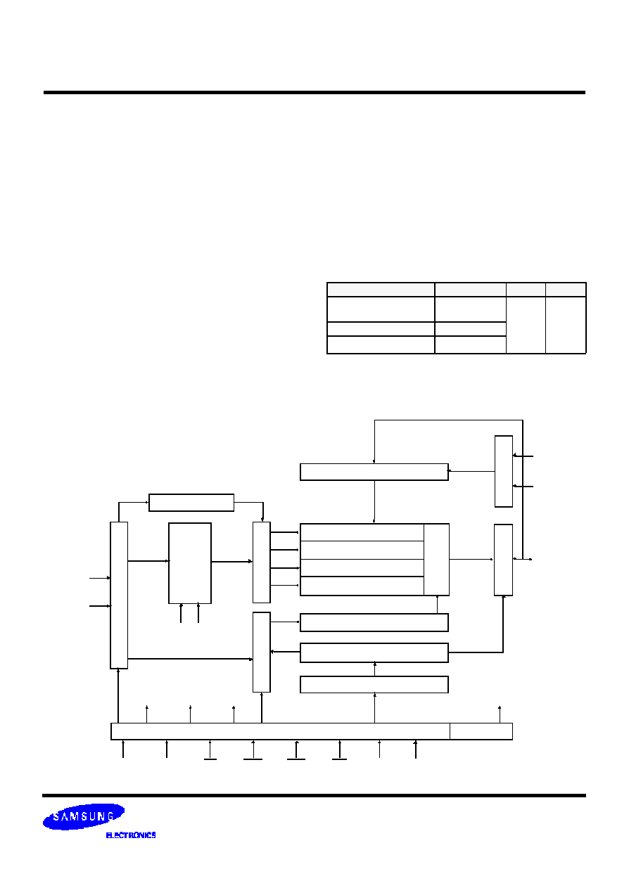
The K4S281633D is 134,217,728 bits synchronous high data
rate Dynamic RAM organized as 4 x 2,097,152 words by 16
bits, fabricated with SAMSUNG
s high performance CMOS
technology. Synchronous design allows precise cycle control
with the use of system clock and I/O transactions are possible
on every clock cycle. Range of operating frequencies, program-
mable burst length and programmable latencies allow the same
device to be useful for a variety of high bandwidth, high perfor-
mance memory system applications.
GENERAL DESCRIPTION
2M x 16Bit x 4 Banks SDRAM in 54CSP
Bank Select
Data Input Register
2M x 16
2M x 16
S
e
n
s
e
A
M
P
O
u
t
p
u
t
B
u
f
f
e
r
I
/
O
C
o
n
t
r
o
l
Column Decoder
Latency & Burst Length
Programming Register
A
d
d
r
e
s
s
R
e
g
i
s
t
e
r
R
o
w
B
u
f
f
e
r
R
e
f
r
e
s
h
C
o
u
n
t
e
r
R
o
w
D
e
c
o
d
e
r
C
o
l
.
B
u
f
f
e
r
L
R
A
S
L
C
B
R
LCKE
LRAS
LCBR
LWE
LDQM
CLK
CKE
CS
RAS
CAS
WE
LDQM
LWE
LDQM
DQi
CLK
ADD
LCAS
LWCBR
2M x 16
2M x 16
Timing Register
UDQM
* Samsung Electronics reserves the right to change products or specification without notice.
FUNCTIONAL BLOCK DIAGRAM
ORDERING INFORMATION
-R(B)L : Low Power, Operating Temperature : -25
∞
C~70
∞
C.
-R(B)N : Low Power, Operating Temperature : -25
∞
C~85
∞
C.
-R(B)P : Low Power, Operating Temperature : -40
∞
C ~ 85
∞
C.
Note :
1. In case of 40MHz Frequency, CL1 can be supported.
Part No.
Max Freq.
Interface Package
K4S281633D-R(B)L/N/P75
133MHz(CL=3)
105MHz(CL=2)
LVCMOS
54 CSP
P b
(Pb Free)
K4S281633D-R(B)L/N/P1H 105MHz(CL=2)
K4S281633D-R(B)L/N/P1L 105MHz(CL=3)
*1
K4S281633D-R(B)L/N/P
Rev. 1.3 Dec. 2002
CMOS SDRAM
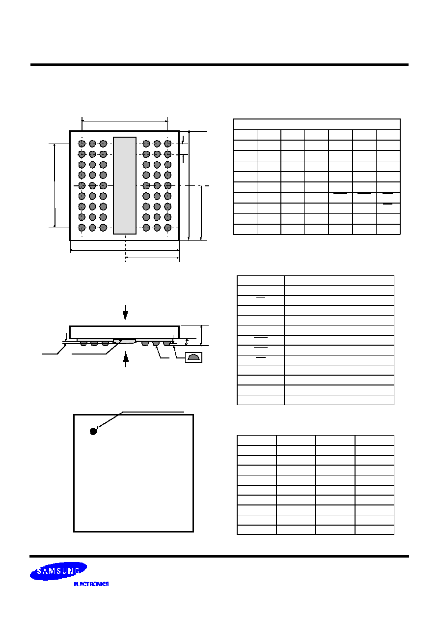
54Ball(6x9) CSP
1
2
3
7
8
9
A
V
SS
DQ15
V
SSQ
V
DDQ
DQ0
V
D D
B
DQ14
DQ13
V
DDQ
V
SSQ
DQ2
DQ1
C
DQ12
DQ11
V
SSQ
V
DDQ
DQ4
DQ3
D
DQ10
DQ9
V
DDQ
V
SSQ
DQ6
DQ5
E
DQ8
NC
V
SS
V
D D
LDQM
DQ7
F
UDQM
CLK
CKE
CAS
RAS
WE
G
NC
A11
A9
BA0
BA1
CS
H
A8
A7
A6
A0
A1
A10
J
V
SS
A5
A4
A3
A2
V
D D
Pin Name
Pin Function
CLK
System Clock
CS
Chip Select
CKE
Clock Enable
A
0
~ A
11
Address
BA
0
~ BA
1
Bank Select Address
RAS
Row Address Strobe
CAS
Column Address Strobe
WE
Write Enable
L(U)DQM
Data Input/Output Mask
DQ
0
~
15
Data Input/Output
V
DD
/V
SS
Power Supply/Ground
V
DDQ
/V
SSQ
Data Output Power/Ground
Package Dimension and Pin Configuration
< Bottom View
*1
>
< Top View
*2
>
< Top View
*2
>
*2: Top View
Symbol
Min
Typ
Max
A
0.90
0.95
1.00
A
1
0.30
0.35
0.40
E
-
8.00
-
E
1
-
6.40
-
D
-
8.00
-
D
1
-
6.40
-
e
-
0.80
-
b
0.40
0.45
0.50
z
-
-
0.10
[Unit:mm]
5
2
1
6
3
4
8
9
7
F
E
D
C
B
J
H
G
A
e
D
D
/
2
D
1
E
1
E
E/2
A
A1
z
b
Encapsulant
Max. 0.20
#A1 Ball Origin Indicator
*1: Bottom View
K
4
S
2
8
1
6
3
3
D
-
X
X
X
X
S
A
M
S
U
N
G
W
e
e
k
K4S281633D-R(B)L/N/P
Rev. 1.3 Dec. 2002
CMOS SDRAM
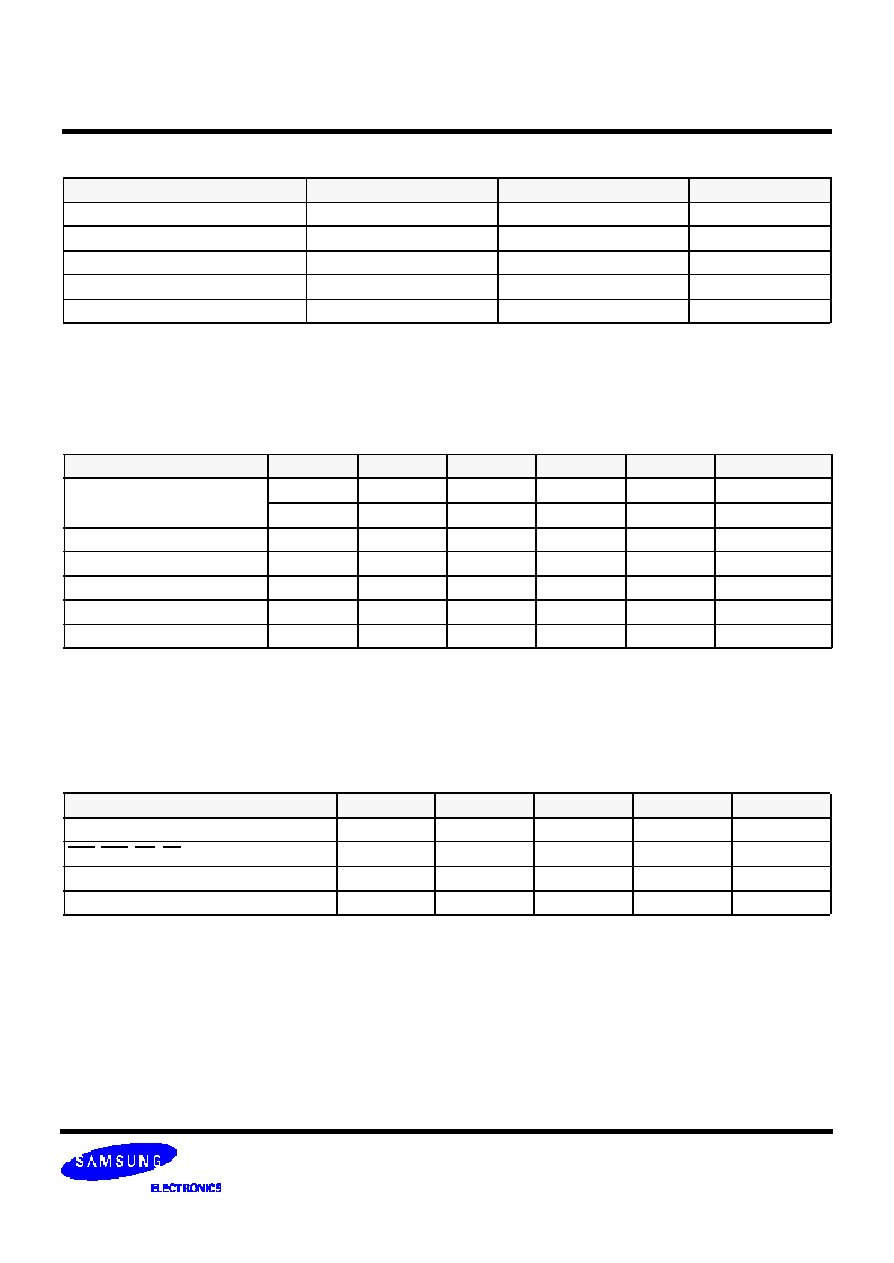
DC OPERATING CONDITIONS
Recommended operating conditions(Voltage referenced to V
SS
= 0V, T
A
=Commercial, Extended, Industrial Temperature)
Notes
:
1. V
IH
(max) = 5.3V AC. The overshoot voltage duration is
3ns.
2. V
IL
(min) = -2.0V AC. The undershoot voltage duration is
3ns.
3. Any input 0V
V
IN
V
DDQ
.
Input leakage currents include HI-Z output leakage for all bi-directional buffers with Tri-State outputs.
4. Dout is disabled, 0V
V
OUT
V
DDQ.
Parameter
Symbol
Min
Typ
Max
Unit
Note
Supply voltage
V
D D
2.7
3.0
3.6
V
V
DDQ
2.7
3.0
3.6
V
Input logic high voltage
V
I H
2.2
3.0
V
DDQ
+0.3
V
1
Input logic low voltage
V
IL
-0.3
0
0.5
V
2
Output logic high voltage
V
O H
2.4
-
-
V
I
O H
= -2mA
Output logic low voltage
V
OL
-
-
0.4
V
I
OL
= 2mA
Input leakage current
I
LI
-10
-
10
uA
3
CAPACITANCE
(V
D D
= 3.0V & 3.3V, T
A
= 23
∞
C, f = 1MHz, V
REF
=0.9V
±
50
mV)
Pin
Symbol
Min
Max
Unit
Note
Clock
C
CLK
2.0
4.0
pF
RAS, CAS, WE, CS, CKE, DQM
C
IN
2.0
4.0
pF
Address
C
ADD
2.0
4.0
pF
DQ
0
~ DQ
15
C
OUT
3.5
6.0
pF
ABSOLUTE MAXIMUM RATINGS
Notes
:
Permanent device damage may occur if ABSOLUTE MAXIMUM RATINGS are exceeded.
Functional operation should be restricted to recommended operating condition.
Exposure to higher than recommended voltage for extended periods of time could affect device reliability.
Parameter
Symbol
Value
Unit
Voltage on any pin relative to Vss
V
I N
, V
OUT
-1.0 ~ 4.6
V
Voltage on V
D D
supply relative to Vss
V
DD
, V
DDQ
-1.0 ~ 4.6
V
Storage temperature
T
STG
-55 ~ +150
∞
C
Power dissipation
P
D
1
W
Short circuit current
I
OS
50
mA
K4S281633D-R(B)L/N/P
Rev. 1.3 Dec. 2002
CMOS SDRAM
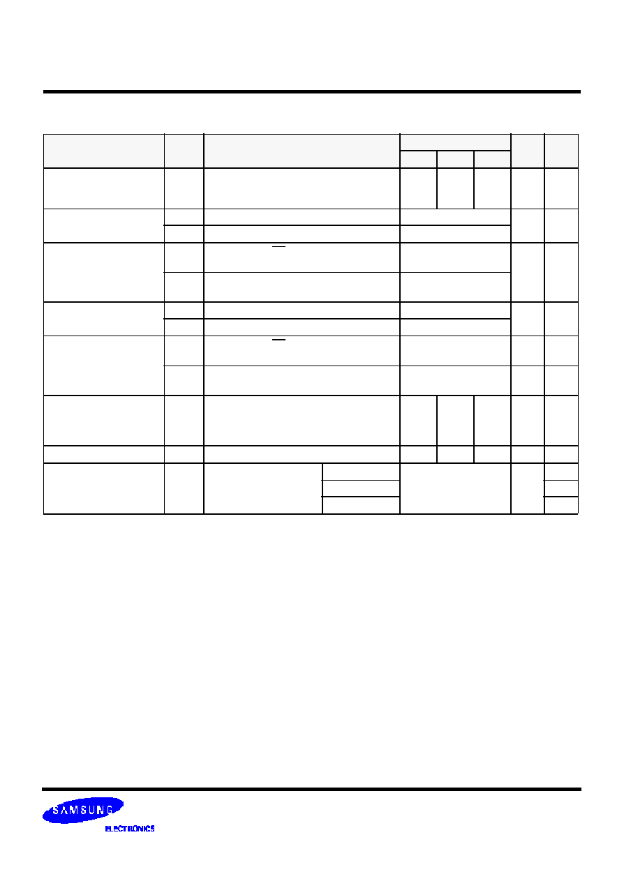
DC CHARACTERISTICS
Recommended operating conditions(Voltage referenced to V
SS
= 0V, T
A
=Commercial, Extended, Industrial Temperature)
Notes :
1. Measured with outputs open.
2. Refresh period is 64ms.
3. K4S281633D-R(B)L**
4. K4S281633D-R(B)N**
5. K4S281633D-R(B)P**
6. Unless otherwise noted, input swing IeveI is CMOS(V
IH
/V
IL
=V
DDQ
/V
SSQ)
Parameter
Symbol
Test Condition
Version
Unit
Note
-75
-1H
-1L
Operating Current
(One Bank Active)
I
CC1
Burst length = 1
t
RC
t
R C
(min)
I
O
= 0 mA
80
75
75
mA
1
Precharge Standby Current
in power-down mode
I
CC2
P
CKE
V
IL
(max), t
CC
= 10ns
0.5
mA
I
CC2
PS CKE & CLK
V
IL
(max), t
CC
=
0.5
Precharge Standby Current
in non power-down mode
I
CC2
N
CKE
V
IH
(min), CS
V
I H
(min), t
CC
= 10ns
Input signals are changed one time during 20ns
12
mA
I
CC2
NS
CKE
V
IH
(min), CLK
V
IL
(max), t
CC
=
Input signals are stable
10
Active Standby Current
in power-down mode
I
CC3
P
CKE
V
IL
(max), t
CC
= 10ns
7
mA
I
CC3
PS CKE & CLK
V
IL
(max), t
CC
=
7
Active Standby Current
in non power-down mode
(One Bank Active)
I
CC3
N
CKE
V
IH
(min), CS
V
I H
(min), t
CC
= 10ns
Input signals are changed one time during 20ns
23
mA
I
CC3
NS
CKE
V
IH
(min), CLK
V
IL
(max), t
CC
=
Input signals are stable
20
mA
Operating Current
(Burst Mode)
I
CC4
I
O
= 0 mA
Page burst
4Banks Activated
t
CCD
= 2CLKs
130
130
110
mA
1
Refresh Current
I
CC5
t
RC
t
RC
(min)
170
170
155
mA
2
Self Refresh Current
I
CC6
CKE
0.2V
-R(B)L
500
uA
3
-R(B)N
4
-R(B)P
5