
K4S643232C
CMOS SDRAM
REV. 1.1 Nov. '99
- 1 -
2M x 32 SDRAM
Revision 1.1
November 1999
512K x 32bit x 4 Banks
Synchronous DRAM
LVTTL
Samsung Electronics reserves the right to change products or specification without notice.

K4S643232C
CMOS SDRAM
REV. 1.1 Nov. '99
- 2 -
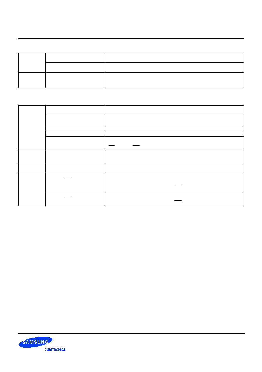
Revision 1.1 (November 17th, 1999)
∑ Corrected typo in ordering information on page 3
Revision 1.0 (October, 1999)
∑ Changed part number from KM432S2030CT-G/F to K4S643232C-TC/TL according to re-organized code system
Revision History
K4S643232C
CMOS SDRAM
REV. 1.1 Nov. '99
- 3 -
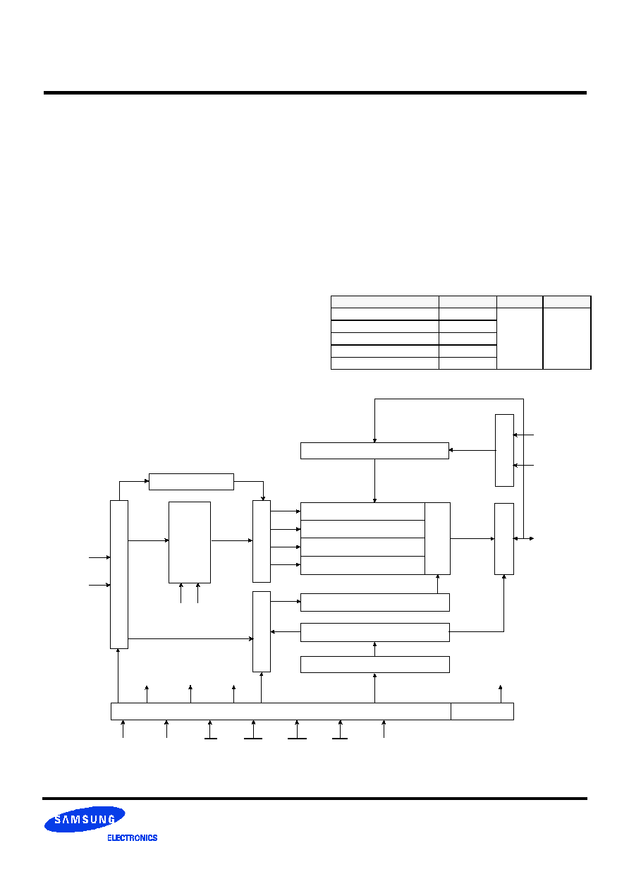
The K4S643232C is 67,108,864 bits synchronous high data
rate Dynamic RAM organized as 4 x 524,288 words by 32 bits,
fabricated with SAMSUNG
s high performance CMOS technol-
ogy. Synchronous design allows precise cycle control with the
use of system clock. I/O transactions are possible on every
clock cycle. Range of operating frequencies, programmable
burst length and programmable latencies allow the same device
to be useful for a variety of high bandwidth, high performance
memory system applications.
∑ 3.3V power supply
∑
LVTTL compatible with multiplexed address
∑
Four banks operation
∑
MRS cycle with address key programs
-. CAS latency (2 & 3)
-. Burst length (1, 2, 4, 8 & Full page)
-. Burst type (Sequential & Interleave)
∑
All inputs are sampled at the positive going edge of the system
clock
∑ Burst read single-bit write operation
∑
DQM for masking
∑ Auto & self refresh
∑
15.6us refresh duty cycle
GENERAL DESCRIPTION
FEATURES
512K x 32Bit x 4 Banks Synchronous DRAM
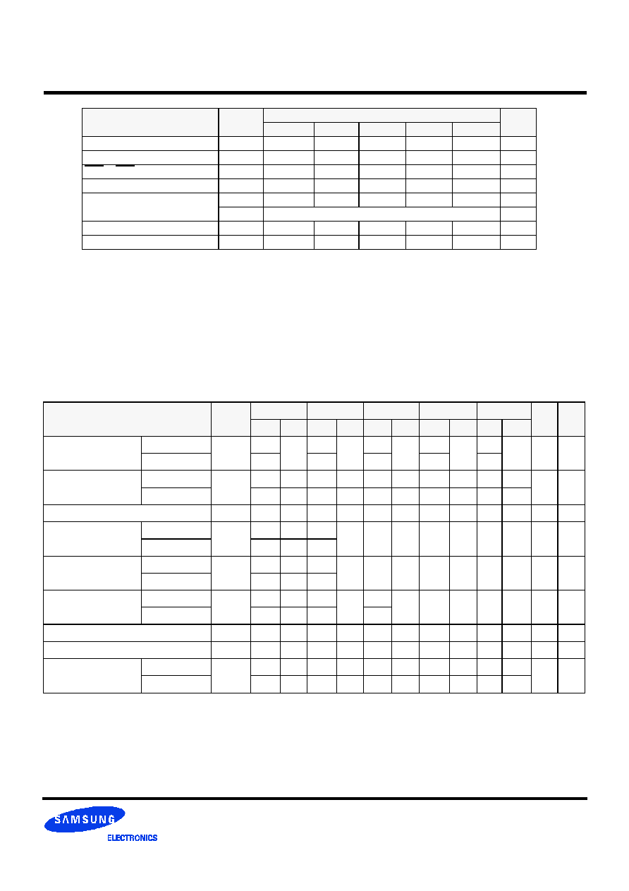
ORDERING INFORMATION
Part NO.
Max Freq.
Interface
Package
K4S643232C-TC/L55
183MHz
LVTTL
86
TSOP(II)
K4S643232C-TC/L60
166MHz
K4S643232C-TC/L70
143MHz
K4S643232C-TC/L80
125MHz
K4S643232C-TC/L10
100MHz
FUNCTIONAL BLOCK DIAGRAM
Samsung Electronics reserves the right to
change products or specification without
notice.
*
Bank Select
Data Input Register
512K x 32
512K x 32
S
e
n
s
e
A
M
P
O
u
t
p
u
t
B
u
f
f
e
r
I
/
O
C
o
n
t
r
o
l
Column Decoder
Latency & Burst Length
Programming Register
A
d
d
r
e
s
s
R
e
g
i
s
t
e
r
R
o
w
B
u
f
f
e
r
R
e
f
r
e
s
h
C
o
u
n
t
e
r
R
o
w
D
e
c
o
d
e
r
C
o
l
.
B
u
f
f
e
r
L
R
A
S
L
C
B
R
LCKE
LRAS
LCBR
LWE
LDQM
CLK
CKE
CS
RAS
CAS
WE
DQM
LWE
LDQM
DQi
CLK
ADD
LCAS
LWCBR
512K x 32
512K x 32
Timing Register
K4S643232C
CMOS SDRAM
REV. 1.1 Nov. '99
- 4 -
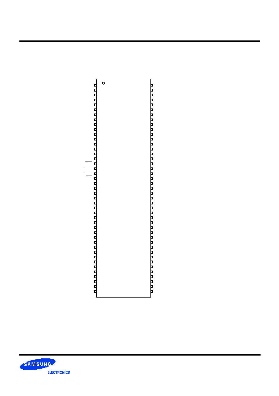
PIN CONFIGURATION (Top view)
V
DD
DQ0
V
DDQ
DQ1
DQ2
V
SSQ
DQ3
DQ4
V
DDQ
DQ5
DQ6
V
SSQ
DQ7
N.C
V
DD
DQM0
WE
CAS
RAS
CS
N.C
BA0
BA1
A10/AP
A0
A1
A2
DQM2
V
DD
N.C
DQ16
V
SSQ
DQ17
DQ18
V
DDQ
DQ19
DQ20
V
SSQ
DQ21
DQ22
V
DDQ
DQ23
V
DD
1
2
3
4
5
6
7
8
9
10
11
12
13
14
15
16
17
18
19
20
21
22
23
24
25
26
27
28
29
30
31
32
33
34
35
36
37
38
39
40
41
42
43
86
85
84
83
82
81
80
79
78
77
76
75
74
73
72
71
70
69
68
67
66
65
64
63
62
61
60
59
58
57
56
55
54
53
52
51
50
49
48
47
46
45
44
V
SS
DQ15
V
SSQ
DQ14
DQ13
V
DDQ
DQ12
DQ11
V
SSQ
DQ10
DQ9
V
DDQ
DQ8
N.C
V
SS
DQM1
N.C
N.C
CLK
CKE
A9
A8
A7
A6
A5
A4
A3
DQM3
V
SS
N.C
DQ31
V
DDQ
DQ30
DQ29
V
SSQ
DQ28
DQ27
V
DDQ
DQ26
DQ25
V
SSQ
DQ24
V
SS
86Pin TSOP (II)
(400mil x 875mil)
(0.5 mm Pin pitch)
K4S643232C
CMOS SDRAM
REV. 1.1 Nov. '99
- 5 -
ABSOLUTE MAXIMUM RATINGS
Parameter
Symbol
Value
Unit
Voltage on any pin relative to Vss
V
IN
, V
OUT
-1.0 ~ 4.6
V
Voltage on V
DD
supply relative to Vss
V
DD
, V
DDQ
-1.0 ~ 4.6
V
Storage temperature
T
STG
-55 ~ +150
∞
C
Power dissipation
P
D
1
W
Short circuit current
I
OS
50
mA
Permanent device damage may occur if "ABSOLUTE MAXIMUM RATINGS" are exceeded.
Functional operation should be restricted to recommended operating condition.
Exposure to higher than recommended voltage for extended periods of time could affect device reliability.
Note :
PIN FUNCTION DESCRIPTION
Pin
Name
Input Function
CLK
System clock
Active on the positive going edge to sample all inputs.
CS
Chip select
Disables or enables device operation by masking or enabling all inputs except
CLK, CKE and DQM.
CKE
Clock enable
Masks system clock to freeze operation from the next clock cycle.
CKE should be enabled at least one cycle prior to new command.
Disables input buffers for power down mode.
A
0
~ A
10
Address
Row/column addresses are multiplexed on the same pins.
Row address : RA
0
~ RA
10
, Column address : CA
0
~ CA
7
BA0,1
Bank select address
Selects bank to be activated during row address latch time.
Selects bank for read/write during column address latch time.
RAS
Row address strobe
Latches row addresses on the positive going edge of the CLK with RAS low.
Enables row access & precharge.
CAS
Column address strobe
Latches column addresses on the positive going edge of the CLK with CAS low.
Enables column access.
WE
Write enable
Enables write operation and row precharge.
Latches data in starting from CAS, WE active.
DQM0 ~ 3
Data input/output mask
Makes data output Hi-Z, t
SHZ
after the clock and masks the output.
Blocks data input when DQM active.
DQ
0
~
31
Data input/output
Data inputs/outputs are multiplexed on the same pins.
V
DD
/V
SS
Power supply/ground
Power and ground for the input buffers and the core logic.
V
DDQ
/V
SSQ
Data output power/ground
Isolated power supply and ground for the output buffers to provide improved noise
immunity.
NC
No Connection
This pin is recommended to be left No connection on the device.
CAPACITANCE
(V
DD
= 3.3V, T
A
= 23
∞
C, f = 1MHz, V
REF
= 1.4V
±
200
mV)
Pin
Symbol
Min
Max
Unit
Clock
C
CLK
2.5
4
pF
RAS, CAS, WE, CS, CKE, DQM
C
IN
2.5
4.5
pF
Address
C
ADD
2.5
4.5
pF
DQ
0
~ DQ
31
C
OUT
4.0
6.5
pF
K4S643232C
CMOS SDRAM
REV. 1.1 Nov. '99
- 6 -
DC CHARACTERISTICS
(Recommended operating condition unless otherwise noted, T
A
= 0 to 70
∞
C)
Parameter
Symbol
Test Condition
CAS
Latency
Version
Unit Note
-55
-60
-70
-80
-10
Operating current
(One bank active)
I
CC1
Burst length = 1
t
RC
t
RC
(min)
I
o
= 0 mA
3
140
140
130
130
115
mA
2
2
-
-
-
130
115
Precharge standby current
in power-down mode
I
CC2
P
CKE
V
IL
(max), t
CC
= 15ns
2
mA
I
CC2
PS
CKE & CLK
V
IL
(max), t
CC
=
2
Precharge standby current
in non power-down mode
I
CC2
N
CKE
V
IH
(min), CS
V
IH
(min), t
CC
= 15ns
Input signals are changed one time during 30ns
20
mA
I
CC2
NS
CKE
V
IH
(min), CLK
V
IL
(max), t
CC
=
Input signals are stable
10
mA
Active standby current in
power-down mode
I
CC3
P
CKE
V
IL
(max), t
CC
= 15ns
3
mA
I
CC3
PS
CKE & CLK
V
IL
(max), t
CC
=
3
Active standby current in
non power-down mode
(One bank active)
I
CC3
N
CKE
V
IH
(min), CS
V
IH
(min), t
CC
= 15ns
Input signals are changed one time during 30ns
30
mA
I
CC3
NS
CKE
V
IH
(min), CLK
V
IL
(max), t
CC
=
Input signals are stable
20
mA
Operating current
(Burst mode)
I
CC4
I
o
= 0 mA
Page burst
2 Banks activated
3
220
200
180
150
130
mA
2
2
-
-
-
130
110
Refresh current
I
CC5
t
RC
t
RC
(min)
3
200
200
180
160
150
mA
3
2
-
-
-
160
150
Self refresh current
I
CC6
CKE
0.2V
2
mA
4
450
uA
5
1. Unless otherwise notes, Input level is CMOS(V
IH
/V
IL
=V
DDQ
/V
SSQ
) in LVTTL.
2. Measured with outputs open.
3. Refresh period is 64ms.
4. K4S643232C-TC**
5. K4S643232C-TL**
Notes :
DC OPERATING CONDITIONS
Recommended operating conditions (Voltage referenced to V
SS
= 0V, T
A
= 0 to 70
∞
C)
Parameter
Symbol
Min
Typ
Max
Unit
Note
Supply voltage
V
DD
, V
DDQ
3.0
3.3
3.6
V
4
Input logic high voltage
V
IH
2.0
3.0
V
DDQ
+0.3
V
1
Input logic low voltage
V
IL
-0.3
0
0.8
V
2
Output logic high voltage
V
OH
2.4
-
-
V
I
OH
= -2mA
Output logic low voltage
V
OL
-
-
0.4
V
I
OL
= 2mA
Input leakage current
I
LI
-10
-
10
uA
3
1. V
IH
(max) = 5.6V AC.The overshoot voltage duration is
3ns.
2. V
IL
(min) = -2.0V AC. The undershoot voltage duration is
3ns.
3. Any input 0V
V
IN
V
DDQ
,
Input leakage currents include Hi-Z output leakage for all bi-directional buffers with Tri-State outputs.
4. The VDD condition of K4S643232C-55/60 is 3.135V~3.6V.
Notes :

K4S643232C
CMOS SDRAM
REV. 1.1 Nov. '99
- 7 -
AC OPERATING TEST CONDITIONS
(V
DD
= 3.3V
±
0.3V, T
A
= 0 to 70
∞
C)
Parameter
Value
Unit
AC input levels (Vih/Vil)
2.4/0.4
V
Input timing measurement reference level
1.4
V
Input rise and fall time
tr/tf = 1/1
ns
Output timing measurement reference level
1.4
V
Output load condition
See Fig. 2
3.3V
1200
870
Output
50pF
*1
V
OH
(DC) = 2.4V, I
OH
= -2mA
V
OL
(DC) = 0.4V, I
OL
= 2mA
Vtt = 1.4V
50
Output
50pF
*1
Z0 = 50
(Fig. 2) AC output load circuit
(Fig. 1) DC output load circuit
1. The DC/AC Test Output Load of K4S643232C-55/60/70 is 30pF.
2. The VDD condition of K4S643232C-55/60 is 3.135V~3.6V.
Note :
OPERATING AC PARAMETER
1. The minimum number of clock cycles is determined by dividing the minimum time required with clock cycle time and then
rounding off to the next higher integer. Refer to the following ns-unit based AC table.
Note :
(AC operating conditions unless otherwise noted)
Parameter
Symbol
Version
Unit
Note
-55
-60
-70
-80
-10
CAS Latency
CL
3
2
3
2
3
2
3
2
3
2
CLK
CLK cycle time
t
CC(min)
5.5
-
6
-
7
-
8
10
10
12
ns
Row active to row active delay
t
RRD(min)
2
CLK
1
RAS to CAS delay
t
RCD(min)
3
-
3
-
3
-
3
2
2
2
CLK
1
Row precharge time
t
RP(min)
3
-
3
-
3
-
3
2
2
2
CLK
1
Row active time
t
RAS(min)
7
-
7
-
7
-
6
5
5
4
CLK
1
t
RAS(max)
100
us
Row cycle time
t
RC
(
min
)
10
-
10
-
10
-
9
7
7
6
CLK
1
Row cycle time in Auto refresh
t
RFC
(
min
)
12
-
12
-
10
-
9
7
7
6
CLK
1,6
Last data in to row precharge
t
RDL(min)
2
CLK
2, 5
Last data in to new col.address delay
t
CDL(min)
1
CLK
2
Last data in to burst stop
t
BDL(min)
1
CLK
2
Col. address to col. address delay
t
CCD(min)
1
CLK
Mode Register Set cycle time
t
MRS(min)
2
CLK
Number of valid output data
CAS Latency=3
2
ea
4
CAS Latency=2
1
K4S643232C
CMOS SDRAM
REV. 1.1 Nov. '99
- 8 -
1. Parameters depend on programmed CAS latency.
2. If clock rising time is longer than 1ns, (tr/2-0.5)ns should be added to the parameter.
3. Assumed input rise and fall time (tr & tf)=1ns.
If tr & tf is longer than 1ns, transient time compensation should be considered,
i.e., [(tr + tf)/2-1]ns should be added to the parameter.
Note :
AC CHARACTERISTICS
(AC operating conditions unless otherwise noted)
Parameter
Symbol
-55
-60
-70
-80
-10
Unit Note
Min
Max
Min
Max
Min
Max
Min
Max
Min
Max
CLK cycle time
CAS Latency=3
t
CC
5.5
1000
6
1000
7
1000
8
1000
10
1000
ns
1
CAS Latency=2
-
-
-
10
12
CLK to valid
output delay
CAS Latency=3
t
SAC
-
5
-
5.5
-
5.5
-
6
-
6
ns
1, 2
CAS Latency=2
-
-
-
-
-
-
-
6
-
8
Output data
t
OH
2
-
2.5
-
2.5
-
2.5
-
2.5
-
ns
2
CLK high pulse width
CAS Latency=3
t
CH
2
-
2.5
-
3
-
3
-
3.5
-
ns
3
CAS Latency=2
-
-
-
CLK low pulse width
CAS Latency=3
t
CL
2
-
2.5
-
3
-
3
-
3.5
-
ns
3
CAS Latency=2
-
-
-
Input setup time
CAS Latency=3
t
SS
1.5
-
1.5
-
1.75
-
2
-
2.5
-
ns
3
CAS Latency=2
-
-
-
-
Input hold time
t
SH
1
-
1
-
1
-
1
-
1
-
ns
3
CLK to output in Low-Z
t
SLZ
1
-
1
-
1
-
1
-
1
-
ns
2
CLK to output
in Hi-Z
CAS Latency=3
t
SHZ
-
5
-
5.5
-
5.5
-
6
-
6
ns
CAS Latency=2
-
-
-
-
-
-
-
6
-
8
2. Minimum delay is required to complete write.
3. All parts allow every cycle column address change.
4. In case of row precharge interrupt, auto precharge and read burst stop.
5. For -55/60/70/80/10, tRDL=1CLK product can be supported within restricted amounts and it will be distinguished by bucket
code "NV". From the next generation, tRDL will be only 2CLK for every clock frequency.
6. A new command should be issued after self refersh exit followed by tRFC.
Parameter
Symbol
Version
Unit
-55
-60
-70
-80
-10
CLK cycle time
t
CC(min)
5.5
6
7
8
10
ns
Row active to row active delay
t
RRD(min)
11
12
14
16
20
ns
RAS to CAS delay
t
RCD(min)
16.5
18
21
20
20
ns
Row precharge time
t
RP(min)
16.5
18
21
20
20
ns
Row active time
t
RAS(min)
38.5
42
49
48
48
ns
t
RAS(max)
100
us
Row cycle time
t
RC
(
min
)
55
60
70
70
70
ns
Row cycle time in Auto refresh
t
RFC
(
min
)
66
72
70
70
70
ns
K4S643232C
CMOS SDRAM
REV. 1.1 Nov. '99
- 9 -
SIMPLIFIED TRUTH TABLE
(V=Valid, X=Don
t care, H=Logic high, L=Logic low)
Command
CKEn-1
CKEn
CS
RAS
CAS
WE
DQM
BA
0,1
A
10
/AP
,
A
9
~ A
0
Note
Register
Mode register set
H
X
L
L
L
L
X
OP code
1,2
Refresh
Auto refresh
H
H
L
L
L
H
X
X
3
Self
refresh
Entry
L
3
Exit
L
H
L
H
H
H
X
X
3
H
X
X
X
3
Bank active & row addr.
H
X
L
L
H
H
X
V
Row address
Read &
column address
Auto precharge disable
H
X
L
H
L
H
X
V
L
Column
address
(A
0
~ A
7
)
4
Auto precharge enable
H
4,5
Write &
column address
Auto precharge disable
H
X
L
H
L
L
X
V
L
Column
address
(A
0
~ A
7
)
4
Auto precharge enable
H
4,5
Burst Stop
H
X
L
H
H
L
X
X
6
Precharge
Bank selection
H
X
L
L
H
L
X
V
L
X
All banks
X
H
Clock suspend or
active power down
Entry
H
L
H
X
X
X
X
X
L
V
V
V
Exit
L
H
X
X
X
X
X
Precharge power down mode
Entry
H
L
H
X
X
X
X
X
L
H
H
H
Exit
L
H
H
X
X
X
X
L
V
V
V
DQM
H
V
X
7
No operation command
H
X
H
X
X
X
X
X
L
H
H
H
1. OP Code : Operand code
A
0
~ A
10
& BA
0
~ BA
1
: Program keys. (@ MRS)
2. MRS can be issued only at all banks precharge state.
A new command can be issued after 2 CLK cycles of MRS.
3. Auto refresh functions are as same as CBR refresh of DRAM.
The automatical precharge without row precharge command is meant by "Auto".
Auto/self refresh can be issued only at all banks precharge state.
4. BA
0
~ BA
1
: Bank select addresses.
If both BA
0
and BA
1
are "Low" at read, write, row active and precharge, bank A is selected.
If both BA
0
is "Low" and BA
1
is "High" at read, write, row active and precharge, bank B is selected.
If both BA
0
is "High" and BA
1
is "Low" at read, write, row active and precharge, bank C is selected.
If both BA
0
and BA
1
are "High" at read, write, row active and precharge, bank D is selected.
If A
10
/AP is "High" at row precharge, BA
0
and BA
1
is ignored and all banks are selected.
5. During burst read or write with auto precharge, new read/write command can not be issued.
Another bank read/write command can be issued after the end of burst.
New row active of the associated bank can be issued at t
RP
after the end of burst.
6. Burst stop command is valid at every burst length.
7. DQM sampled at positive going edge of a CLK and masks the data-in at the very CLK (Write DQM latency is 0),
but makes Hi-Z state the data-out of 2 CLK cycles after. (Read DQM latency is 2)
Notes :
X
K4S643232C
CMOS SDRAM
REV. 1.1 Nov. '99
- 10
MODE REGISTER FIELD TABLE TO PROGRAM MODES
Register Programmed with MRS
Address
Function
A
10
/AP
RFU
A
9
W.B.L
A
8
A
7
TM
A
6
A
5
A
4
A
3
A
2
A
1
A
0
CAS Latency
BT
Burst Length
A
8
A
7
A
6
A
5
A
4
A
3
A
2
A
1
A
0
BT = 0
Test Mode
Type
Mode Register Set
Reserved
Reserved
Reserved
0
0
1
1
0
1
0
1
Write Burst Length
A
9
0
1
Length
Burst
Single Bit
Latency
Reserved
Reserved
2
3
Reserved
Reserved
Reserved
Reserved
CAS Latency
0
0
0
0
1
1
1
1
0
0
1
1
0
0
1
1
0
1
0
1
0
1
0
1
Burst Type
0
1
BT = 1
Burst Length
Type
Sequential
Interleave
0
0
0
0
1
1
1
1
0
0
1
1
0
0
1
1
0
1
0
1
0
1
0
1
1
2
4
8
Reserved
Reserved
Reserved
Full Page
1
2
4
8
Reserved
Reserved
Reserved
Reserved
POWER UP SEQUENCE
SDRAMs must be powered up and initialized in a predefined manner to prevent undefined operations.
1. Apply power and start clock. Must maintain CKE= "H", DQM= "H" and the other pins are NOP condition at the inputs.
2. Maintain stable power, stable clock and NOP input condition for a minimum of 200us.
3. Issue precharge commands for all banks of the devices.
4. Issue 2 or more auto-refresh commands.
5. Issue a mode register set command to initialize the mode register.
cf.) Sequence of 4 & 5 is regardless of the order.
The device is now ready for normal operation.
Note : 1. If A
9
is high during MRS cycle, "Burst Read Single Bit Write" function will be enabled.
2. RFU (Reserved for future use) should stay "0" during MRS cycle.
Full Page Length : x32 (256)
BA
0
~ BA
1
RFU
K4S643232C
CMOS SDRAM
REV. 1.1 Nov. '99
- 11
BURST SEQUENCE (BURST LENGTH = 4)
Initial Address
Sequential
Interleave
A
1
A
0
0
0
1
1
0
1
0
1
0
1
2
3
1
2
3
0
2
3
0
1
3
0
1
2
0
1
2
3
1
0
3
2
2
3
0
1
3
2
1
0
BURST SEQUENCE (BURST LENGTH = 8)
Initial Address
Sequential
Interleave
0
0
0
0
1
1
1
1
0
1
0
1
0
1
0
1
0
1
2
3
4
5
6
7
2
3
4
5
6
7
0
1
4
5
6
7
0
1
2
3
6
7
0
1
2
3
4
5
A
1
A
0
A
2
0
0
1
1
0
0
1
1
1
2
3
4
5
6
7
0
3
4
5
6
7
0
1
2
5
6
7
0
1
2
3
4
7
0
1
2
3
4
5
6
0
1
2
3
4
5
6
7
2
3
0
1
6
7
4
5
4
5
6
7
0
1
2
3
6
7
4
5
2
3
0
1
1
0
3
2
5
4
7
6
3
2
1
0
7
6
5
4
5
4
7
6
1
0
3
2
7
6
5
4
3
2
1
0

K4S643232C
CMOS SDRAM
REV. 1.1 Nov. '99
- 12
DEVICE OPERATIONS
NOP and DEVICE DESELECT
When RAS, CAS and WE are high, the SDRAM performs no
operation (NOP). NOP does not initiate any new operation, but
is needed to complete operations which require more than sin-
gle clock cycle like bank activate, burst read, auto refresh, etc.
The device deselect is also a NOP and is entered by asserting
CS high. CS high disables the command decoder so that RAS,
CAS, WE and all the address inputs are ignored.
POWER-UP
SDRAMs must be powered up and initialized in a pre-
defined manner to prevent undefined operations.
1. Apply power and start clock. Must maintain CKE= "H", DQM=
"H" and the other pins are NOP condition at the inputs.
2. Maintain stable power, stable clock and NOP input condition
for a minimum of 200us.
3. Issue precharge commands for both banks of the devices.
4. Issue 2 or more auto-refresh commands.
5. Issue a mode register set command to initialize the mode reg-
ister.
cf.) Sequence of 4 & 5 is regardless of the order.
The device is now ready for normal operation.
CLOCK (CLK)
The clock input is used as the reference for all SDRAM opera-
tions. All operations are synchronized to the positive going edge
of the clock. The clock transitions must be monotonic between
V
IL
and V
IH
. During operation with CKE high all inputs are
assumed to be in a valid state (low or high) for the duration of
set-up and hold time around positive edge of the clock in order
to function well Q perform and I
CC
specifications.
CLOCK ENABLE (CKE)
The clock enable(CKE) gates the clock onto SDRAM. If CKE
goes low synchronously with clock (set-up and hold time are the-
same as other inputs), the internal clock is suspended from the
next clock cycle and the state of output and burst address is fro-
zen as long as the CKE remains low. All other inputs are ignored
from the next clock cycle after CKE goes low. When all banks
are in the idle state and CKE goes low synchronously with clock,
the SDRAM enters the power down mode from the next clock
cycle. The SDRAM remains in the power down mode ignoring
the other inputs as long as CKE remains low. The power down
exit is synchronous as the internal clock is suspended. When
CKE goes high at least "1CLK + t
SS
" before the high going edge
of the clock, then the SDRAM becomes active from the same
clock edge accepting all the input commands.
BANK ADDRESSES (BA0 ~ BA1)
This SDRAM is organized as four independent banks of 524,288
words x 32 bits memory arrays. The BA
0
~ BA
1
inputs are
latched at the time of assertion of RAS and CAS to select the
bank to be used for the operation. The bank addresses BA
0
~
BA
1
are latched at bank active, read, write, mode register set
and precharge operations.
ADDRESS INPUTS (A0 ~ A10)
The 19 address bits are required to decode the 524,288 word
locations are multiplexed into 11 address input pins (A
0
~ A
10
).
The 11 bit row addresses are latched along with RAS and BA
0
~
BA
1
during bank activate command. The 8 bit column addresses
are latched along with CAS, WE and BA
0
~ BA
1
during read or
write command.

K4S643232C
CMOS SDRAM
REV. 1.1 Nov. '99
- 13
MODE REGISTER SET (MRS)
The mode register stores the data for controlling the various
operating modes of SDRAM. It programs the CAS latency, burst
type, burst length, test mode and various vendor specific options
to make SDRAM useful for variety of different applications. The
default value of the mode register is not defined, therefore the
mode register must be written after power up to operate the
SDRAM. The mode register is written by asserting low on CS,
RAS, CAS and WE (The SDRAM should be in active mode with
CKE already high prior to writing the mode register). The state of
address pins A
0
~ A
10
and BA
0
~ BA
1
in the same cycle as CS,
RAS, CAS and WE going low is the data written in the mode
register. Two clock cycles is required to complete the write in the
mode register. The mode register contents can be changed
using the same command and clock cycle requirements during
operation as long as all banks are in the idle state. The mode
register is divided into various fields depending on the fields of
functions. The burst length field uses A
0
~ A
2
, burst type uses
A
3
, CAS latency (read latency from column address) use A
4
~
A
6
, vendor specific options or test mode use A
7
~ A
8
, A
10
/AP
and BA
0
~ BA
1
. The write burst length is programmed using A
9
.
A
7
~ A
8
, A
10
/AP and BA
0
~ BA
1
must be set to low for normal
SDRAM operation. Refer to the table for specific codes for vari-
ous burst length, burst type and CAS latencies.
BANK ACTIVATE
The bank activate command is used to select a random row in
an idle bank. By asserting low on RAS and CS with desired row
and bank address, a row access is initiated. The read or write
operation can occur after a time delay of t
RCD
(min) from the time
of bank activation. t
RCD
is an internal timing parameter of
SDRAM, therefore it is dependent on operating clock frequency.
The minimum number of clock cycles required between bank
activate and read or write command should be calculated by
dividing t
RCD
(min) with cycle time of the clock and then rounding
off the result to the next higher integer. The SDRAM has four
internal banks in the same chip and shares part of the internal
circuitry to reduce chip area, therefore it restricts the activation
of four banks simultaneously. Also the noise generated during
sensing of each bank of SDRAM is high, requiring some time for
power supplies to recover before another bank can be sensed
reliably. t
RRD
(min) specifies the minimum time required between
activating different bank. The number of clock cycles required
between different bank activation must be calculated similar to
t
RCD
specification. The minimum time required for the bank to be
active to initiate sensing and restoring the complete row of
dynamic cells is determined by t
RAS
(min). Every SDRAM bank
activate command must satisfy t
RAS
(min) specification before a
precharge command to that active bank can be asserted. The
maximum time any bank can be in the active state is determined
by t
RAS
(max). The number of cycles for both t
RAS
(min) and
t
RAS
(max) can be calculated similar to t
RCD
specification.
BURST READ
The burst read command is used to access burst of data on con-
secutive clock cycles from an active row in an active bank. The
burst read command is issued by asserting low on CS and CAS
with WE being high on the positive edge of the clock. The bank
must be active for at least t
RCD
(min) before the burst read com-
mand is issued. The first output appears in CAS latency number
of clock cycles after the issue of burst read command. The burst
length, burst sequence and latency from the burst read com-
mand is determined by the mode register which is already pro-
grammed. The burst read can be initiated on any column
address of the active row. The address wraps around if the initial
address does not start from a boundary such that number of out-
puts from each I/O are equal to the burst length programmed in
the mode register. The output goes into high-impedance at the
end of the burst, unless a new burst read was initiated to keep
the data output gapless. The burst read can be terminated by
issuing another burst read or burst write in the same bank or the
other active bank or a precharge command to the same bank.
The burst stop command is valid at every page burst length.
BURST WRITE
The burst write command is similar to burst read command and
is used to write data into the SDRAM on consecutive clock
cycles in adjacent addresses depending on burst length and
burst sequence. By asserting low on CS, CAS and WE with valid
column address, a write burst is initiated. The data inputs are
provided for the initial address in the same clock cycle as the
burst write command. The input buffer is deselected at the end
of the burst length, even though the internal writing can be com-
pleted yet. The writing can be completed by issuing a burst read
and DQM for blocking data inputs or burst write in the same or
another active bank. The burst stop command is valid at every
burst length. The write burst can also be terminated by using
DQM for blocking data and procreating the bank t
RDL
after the
last data input to be written into the active row. See DQM
OPERATION also.
DEVICE OPERATIONS (Continued)

K4S643232C
CMOS SDRAM
REV. 1.1 Nov. '99
- 14
DQM OPERATION
The DQM is used to mask input and output operations. It works
similar to OE during read operation and inhibits writing during
write operation. The read latency is two cycles from DQM and
zero cycle for write, which means DQM masking occurs two
cycles later in read cycle and occurs in the same cycle during
write cycle. DQM operation is synchronous with the clock. The
DQM signal is important during burst interruptions of write with
read or precharge in the SDRAM. Due to asynchronous nature
of the internal write, the DQM operation is critical to avoid
unwanted or incomplete writes when the complete burst write is
not required. Please refer to DQM timing diagram also.
PRECHARGE
The precharge operation is performed on an active bank by
asserting low on CS, RAS, WE and A
10
/AP with valid BA
0
~ BA
1
of the bank to be precharged. The precharge command can be
asserted anytime after t
RAS
(min) is satisfied from the bank active
command in the desired bank. t
RP
is defined as the minimum
number of clock cycles required to complete row precharge is
calculated by dividing t
RP
with clock cycle time and rounding up
to the next higher integer. Care should be taken to make sure
that burst write is completed or DQM is used to inhibit writing
before precharge command is asserted. The maximum time any
bank can be active is specified by t
RAS
(max). Therefore, each
bank activate command. At the end of precharge, the bank
enters the idle state and is ready to be activated again. Entry to
Power down, Auto refresh, Self refresh and Mode register set
etc. is possible only when all banks are in idle state.
AUTO PRECHARGE
The precharge operation can also be performed by using auto
precharge. The SDRAM internally generates the timing to satisfy
t
RAS
(min) and "t
RP
" for the programmed burst length and CAS
latency. The auto precharge command is issued at the same
time as burst read or burst write by asserting high on A
10
/AP. If
burst read or burst write by asserting high on A
10
/AP, the bank is
left active until a new command is asserted. Once auto
precahrge command is given, no new commands are possible to
that particular bank until the bank achieves idle state.
BOTH BANKS PRECHARGE
Both banks can be precharged at the same time by using Pre-
charge all command. Asserting low on CS, RAS, and WE with
high on A
10
/AP after all banks have satisfied t
RAS
(min) require-
ment, performs precharge on all banks. At the end of t
RP
after
performing precharge to all the banks, both banks are in idle
state.
DEVICE OPERATIONS (Continued)
AUTO REFRESH
The storage cells of SDRAM need to be refreshed every 64ms
to maintain data. An auto refresh cycle accomplishes refresh of
a single row of storage cells. The internal counter increments
automatically on every auto refresh cycle to refresh all the rows.
An auto refresh command is issued by asserting low on CS,
RAS and CAS with high on CKE and WE. The auto refresh com-
mand can only be asserted with both banks being in idle state
and the device is not in power down mode (CKE is high in the
previous cycle). The time required to complete the auto refresh
operation is specified by t
RFC
(min). The minimum number of
clock cycles required can be calculated by driving t
RFC
with
clock cycle time and them rounding up to the next higher integer.
The auto refresh command must be followed by NOP's until the
auto refresh operation is completed. All banks will be in the idle
state at the end of auto refresh operation. The auto refresh is the
preferred refresh mode when the SDRAM is being used for nor-
mal data transactions. The auto refresh cycle can be performed
once in 15.6us or a burst of 4096 auto refresh cycles once in
64ms.
SELF REFRESH
The self refresh is another refresh mode available in the
SDRAM. The self refresh is the preferred refresh mode for data
retention and low power operation of SDRAM. In self refresh
mode, the SDRAM disables the internal clock and all the input
buffers except CKE. The refresh addressing and timing are
internally generated to reduce power consumption.
The self refresh mode is entered from all banks idle state by
asserting low on CS, RAS, CAS and CKE with high on WE.
Once the self refresh mode is entered, only CKE state being low
matters, all the other inputs including the clock are ignored in
order to remain in the self refresh mode.
The self refresh is exited by restarting the external clock and
then asserting high on CKE. This must be followed by NOP's for
a minimum time of t
RFC
before the SDRAM reaches idle state to
begin normal operation. If the system uses burst auto refresh
during normal operation, it is recommended to use burst 4096
auto refresh cycles immediately after exiting in self refresh
mode.
K4S643232C
CMOS SDRAM
REV. 1.1 Nov. '99
- 15
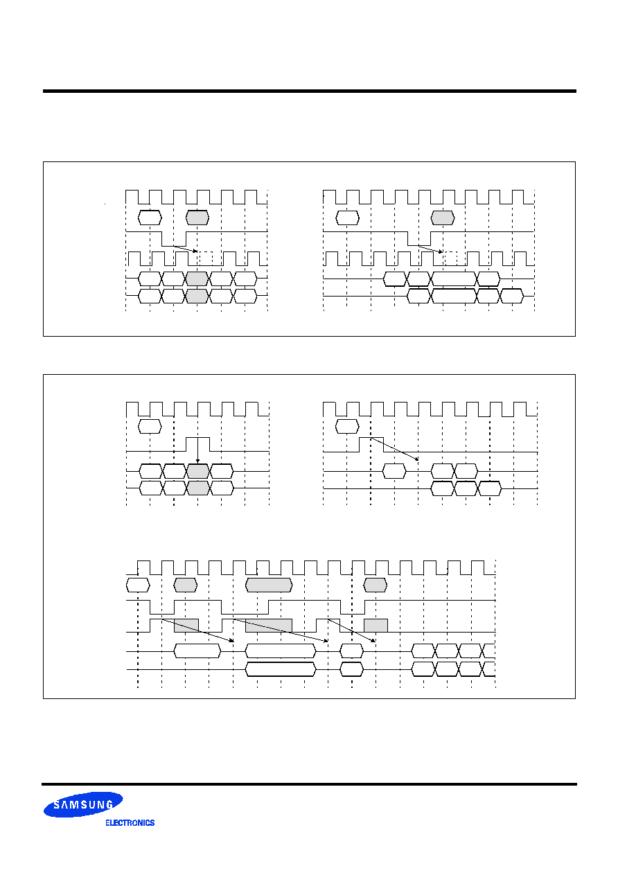
1) Clock Suspended During Write (BL=4
1. CLOCK Suspend
WR
D
0
D
1
D
2
D
3
D
0
D
1
D
2
D
3
CLK
CMD
CKE
Internal
CKE
DQ(CL2)
DQ(CL3)
Masked by CKE
2) Clock Suspended During Read (BL=4)
D
0
Not Written
1) Write Mask (BL=4)
2. DQM Operation
WR
D
0
D
1
D
3
D
0
D
1
D
3
CLK
CMD
DQM
DQ(CL2)
DQ(CL3)
Masked byDQM
2) Read Mask (BL=4)
RD
Q
0
Q
2
Q
3
Q
1
Q
2
Q
3
Masked by DQM
DQM to Data-in Mask = 0
DQM to Data-out Mask = 2
Hi-Z
Hi-Z
3) DQM with Clock Suspended (Full Page Read)
Note 2
RD
CLK
CMD
CKE
DQ(CL2)
DQ(CL3)
Q
0
Q
4
Q
7
Q
8
Q
2
Q
3
Q
6
Q
7
Q
1
Hi-Z
Hi-Z
Hi-Z
Hi-Z
Hi-Z
Hi-Z
DQM
*Note : 1. CKE to CLK disable/enable = 1CLK.
2. DQM makes data out Hi-Z after 2CLKs which should masked by CKE " L"
3. DQM masks both data-in and data-out.
BASIC FEATURE AND FUNCTION DESCRIPTIONS
RD
Q
0
Q
1
Q
2
Q
0
Q
1
Q
2
Q
3
Masked by CKE
Q
3
Suspended Dout
Q
6
Q
5

K4S643232C
CMOS SDRAM
REV. 1.1 Nov. '99
- 16
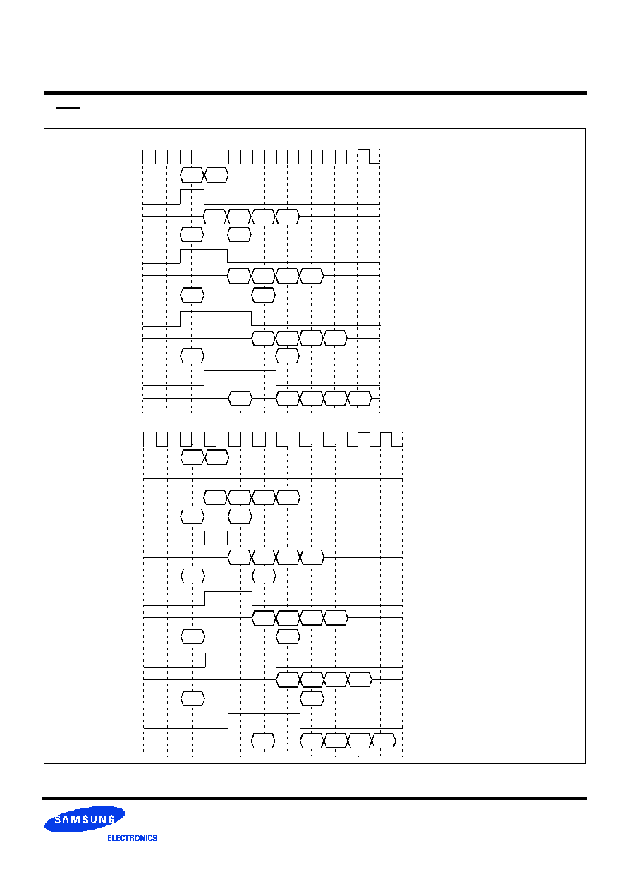
1) Read interrupted by Read (BL=4)
3. CAS Interrupt (I)
CLK
CMD
ADD
Note 1
RD
RD
A
B
QA
0
QB
1
QB
2
QB
3
QB
0
QA
0
QB
1
QB
2
QB
3
QB
0
tCCD
Note 2
2) Write interrupted by Write (BL=2)
3) Write interrupted by Read (BL=2)
WR
WR
A
B
tCCD Note 2
DA
0
DB
1
DB
0
tCDL
Note 3
CLK
CMD
ADD
DQ
WR
RD
A
B
tCCD Note 2
tCDL
Note 3
DA
0
QB
1
QB
0
DA
0
QB
1
QB
0
DQ(CL2)
DQ(CL3)
*Note : 1. By " Interrupt", It is meant to stop burst read/write by external command before the end of burst.
By "CAS Interrupt", to stop burst read/write by CAS access ; read and write.
2. t
CCD
: CAS to CAS delay. (=1CLK)
3. t
CDL
: Last data in to new column address delay. (=1CLK)
DQ(CL2)
DQ(CL3)
K4S643232C
CMOS SDRAM
REV. 1.1 Nov. '99
- 17
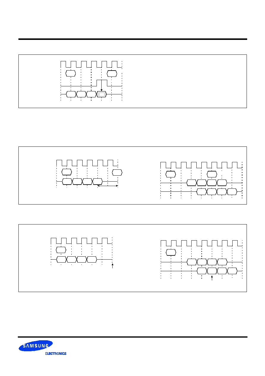
4. CAS Interrupt (II) : Read Interrupted by Write & DQM
*Note : 1. To prevent bus contention, there should be at least one gap between data in and data out.
D
1
D
2
RD
D
3
WR
D
0
D
1
D
2
D
3
D
0
D
1
D
2
D
3
D
0
RD
WR
RD
WR
Hi-Z
Hi-Z
RD
WR
Q
0
D
1
D
2
D
3
D
0
Note 1
Hi-Z
(a) CL=2, BL=4
CLK
i) CMD
DQM
DQ
ii) CMD
DQM
DQ
iii) CMD
DQM
DQ
iv) CMD
DQM
DQ
(b) CL=3, BL=4
CLK
i) CMD
DQM
DQ
D
1
D
2
RD
D
3
WR
D
0
D
1
D
2
D
3
D
0
D
1
D
2
D
3
D
0
RD
WR
RD
WR
D
1
D
2
D
3
D
0
RD
WR
RD
WR
D
1
D
2
D
3
D
0
Hi-Z
ii) CMD
DQM
DQ
iii) CMD
DQM
DQ
iii) CMD
DQM
DQ
iv) CMD
DQM
DQ
Q
0
Note 1
Hi-Z
K4S643232C
CMOS SDRAM
REV. 1.1 Nov. '99
- 18
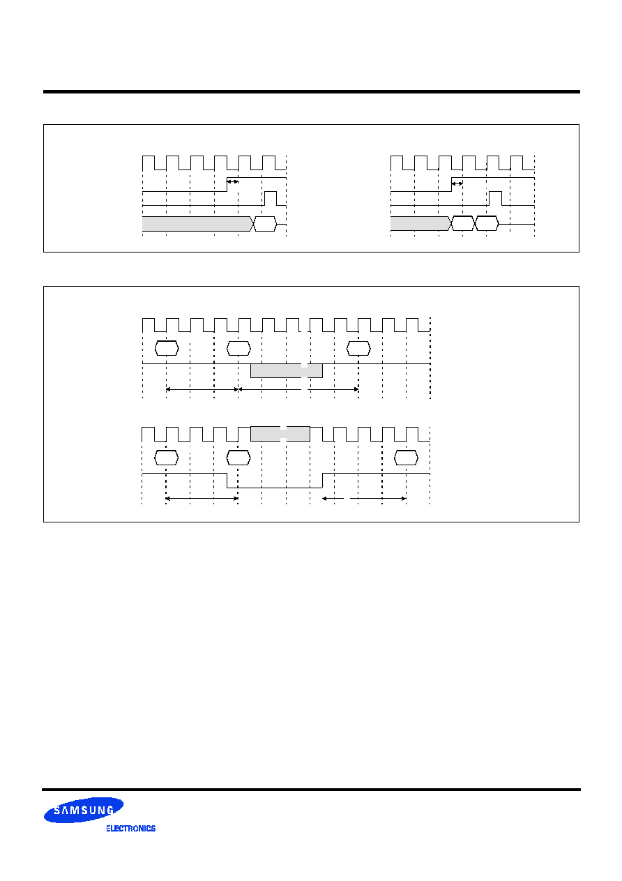
*Note : 1. To prevent bus contention, DQM should be issued which makes at least one gap between data in and data out.
2. To inhibit invalid write, DQM should be issued.
3. This precharge command and burst write command should be of the same bank, otherwise it is not precharge
interrupt but only another bank precharge of four banks operation.
4. For -55/60/70/80/10, tRDL=1CLK product can be supported within restricted amounts and it will be distinguished by bucket code "NV"
. From the next generation, tRDL will be only 2CLK for every clock frequency.
5. Write Interrupted by Precharge & DQM
D
0
D
1
D
2
CLK
CMD
DQM
DQ
Masked by DQM
WR
PRE
D
3
Note 3,4
Note 2
6. Precharge
D
0
D
1
D
2
CLK
CMD
DQ
WR
PRE
D
3
1) Normal Write (BL=4)
tRDL
Note 1,4
2) Normal Read (BL=4)
CLK
CMD
DQ(CL2)
DQ(CL3)
RD
PRE
Q
0
Q
1
Q
2
Q
3
Q
0
Q
1
Q
2
Q
3
1
2
*Note : 1. t
RDL
: Last data in to row precharge delay
2. Number of valid output data after row precharge : 1, 2 for CAS Latency = 2, 3 respectively.
3. The row active command of the precharge bank can be issued after t
RP
from this point.
The new read/write command of other activated bank can be issued from this point.
At burst read/write with auto precharge, CAS interrupt of the same/another bank is illegal.
4. For -55/60/70/80/10, tRDL=1CLK product can be supported within restricted amounts and it will be distinguished by bucket code "NV"
. From the next generation, tRDL will be only 2CLK for every clock frequency
7. Auto Precharge
D
0
D
1
D
2
CLK
CMD
DQ
WR
D
3
1) Normal Write (BL=4)
Note 3,4
Auto Precharge Starts
2) Normal Read (BL=4)
CLK
CMD
DQ(CL2)
DQ(CL3)
RD
D
0
D
1
D
2
D
3
D
0
D
1
D
2
D
3
Note 3
Auto Precharge Starts
Note 2

K4S643232C
CMOS SDRAM
REV. 1.1 Nov. '99
- 19
*Note : 1. t
RDL
: 1 CLK
2. t
BDL
: 1 CLK ; Last data in to burst stop delay.
Read or write burst stop command is valid at every burst length.
3. Number of valid output data after row precharge or burst stop : 1, 2 for CAS latency= 2, 3 respectiviely.
4. PRE : All banks precharge if necessary.
MRS can be issued only at all banks precharge state.
5. For -55/60/70/80/10, tRDL=1CLK product can be supported within restricted amounts and it will be distinguished by bucket code "NV"
. From the next generation, tRDL will be only 2CLK for every clock frequency
8. Burst Stop & Interrupted by Precharge
3) Read Interrupted by Precharge (BL=4)
CLK
CMD
DQ(CL2)
DQ(CL3)
RD
PRE
Q
0
Q
1
Q
0
Q
1
1
2
9. MRS
CLK
PRE
1) Mode Register Set
4) Read Burst Stop (BL=4)
CLK
CMD
DQ(CL2)
DQ(CL3)
RD
STOP
Q
0
Q
1
Q
0
Q
1
1
2
MRS
ACT
Note 4
tRP
2CLK
CMD
D
0
D
1
D
2
CLK
CMD
DQ
WR
PRE
D
3
1) Normal Write (BL=4)
tRDL Note 1,5
D
0
D
1
D
2
CLK
CMD
DQ
WR
STOP
D
3
2) Write Burst Stop (BL=8)
DQM
DQM
tBDL Note 2
D
4
D
5
Note 3
K4S643232C
CMOS SDRAM
REV. 1.1 Nov. '99
- 20
*Note : 1. Active power down : one or more banks active state.
2. Precharge power down : all banks precharge state.
3. The auto refresh is the same as CBR refresh of conventional DRAM.
No precharge commands are required after auto refresh command.
During t
RFC
from auto refresh command, any other command can not be accepted.
4. Before executing auto/self refresh command, all banks must be idle state.
5. MRS, Bank Active, Auto/Self Refresh, Power Down Mode Entry.
6. During self refresh mode, refresh interval and refresh operation are perfomed internally.
After self refresh entry, self refresh mode is kept while CKE is low.
During self refresh mode, all inputs expect CKE will be don't cared, and outputs will be in Hi-Z state.
For the time interval of t
RFC
from self refresh exit command, any other command can not be accepted.
Before/After self refresh mode, burst auto refresh cycle (4096 cycles) is recommended.
10. Clock Suspend Exit & Power Down Exit
CLK
CKE
CMD
RD
1) Clock Suspend (=Active Power Down) Exit
tSS
CLK
CKE
CMD
2) Power Down (=Precharge Power Down) Exit
Note 1
Note 5
Internal
CLK
NOP
tSS
Note 2
Internal
CLK
11. Auto Refresh & Self Refresh
CLK
CMD
1) Auto Refresh & Self Refresh
CKE
PRE
AR
CMD
Note 4
tRP
tRFC
°Û
°Û
°Û
°Û
CLK
CMD
2) Self Refresh
CKE
PRE
SR
CMD
Note 4
tRP
tRFC
°Û
Note 6
Note 3
ACT
°Û
°Û
K4S643232C
CMOS SDRAM
REV. 1.1 Nov. '99
- 21
12. About Burst Type Control
At MRS A
3
= "0". See the BURST SEQUENCE TABLE. (BL=4, 8)
BL=1, 2, 4, 8 and full page.
At MRS A
3
= "1". See the BURST SEQUENCE TABLE. (BL=4, 8)
BL=4, 8. At BL=1, 2 Interleave Counting = Sequential Counting
Every cycle Read/Write Command with random column address can realize Random
Column Access.
That is similar to Extended Data Out (EDO) Operation of conventional DRAM.
Basic
MODE
Random
MODE
Sequential Counting
Interleave Counting
Random column Access
t
CCD
= 1 CLK
13. About Burst Length Control
At MRS A
2,1,0
= "000".
At auto precharge, t
RAS
should not be violated.
At MRS A
2,1,0
= "001".
At auto precharge, t
RAS
should not be violated.
Before the end of burst, Row precharge command of the same bank stops read/write
burst with Row precharge.
t
RDL
= 2 with DQM, valid DQ after burst stop is 1, 2 for CAS latency 2, 3 respectively.
During read/write burst with auto precharge, RAS interrupt can not be issued.
Basic
MODE
Interrupt
MODE
1
2
RAS Interrupt
(Interrupted by Precharge)
At MRS A
2,1,0
= "010".
At MRS A
2,1,0
= "011".
At MRS A
2,1,0
= "111".
Wrap around mode(Infinite burst length) should be stopped by burst stop
Ras interrupt or CAS interrupt
4
8
Full Page
At MRS A
9
= "1".
Read burst =1, 2, 4, 8, full page write Burst =1
At auto precharge of write, t
RAS
should not be violated.
t
BDL
= 1, Valid DQ after burst stop is 1, 2 for CAS latency 2, 3 respectively
Using burst stop command, any burst length control is possible.
Before the end of burst, new read/write stops read/write burst and starts new
read/write burst.
During read/write burst with auto precharge, CAS interrupt can not be issued.
BRSW
Burst Stop
CAS Interrupt
Random
MODE
Special
MODE
K4S643232C
CMOS SDRAM
REV. 1.1 Nov. '99
- 22
X
X
X
CA, A
10
/AP
RA
A
10
/AP
X
OP code
X
X
X
CA, A
10
/AP
CA, A
10
/AP
RA
A
10
/AP
X
X
X
X
CA, A
10
/AP
CA, A
10
/AP
RA
A
10
/AP
X
X
X
X
CA, A
10
/AP
CA, A
10
/AP
RA
A
10
/AP
X
X
X
X
CA, A
10
/AP
RA, RA
10
X
X
X
X
CA, A
10
/AP
RA, RA
10
X
X
X
X
CA
RA
A
10
/AP
FUNCTION TRUTH TABLE (TABLE 1)
Current
State
CS
RAS
CAS
WE
BA
ADDR
ACTION
Note
H
L
L
L
L
L
L
L
H
L
L
L
L
L
L
L
H
L
L
L
L
L
L
L
H
L
L
L
L
L
L
L
H
L
L
L
L
L
H
L
L
L
L
L
H
L
L
L
L
L
IDLE
Row
Active
Read
Write
Read with
Auto
Precharge
Write with
Auto
Precharge
Pre-
charging
NOP
NOP
ILLEGAL
ILLEGAL
Row (& Bank) Active ; Latch RA
NOP
Auto Refresh or Self Refresh
Mode Register Access
NOP
NOP
ILLEGAL
Begin Read ; latch CA ; determine AP
Begin Write ; latch CA ; determine AP
ILLEGAL
Precharge
ILLEGAL
NOP (Continue Burst to End --> Row Active)
NOP (Continue Burst to End --> Row Active)
Term burst --> Row active
Term burst, New Read, Determine AP
Term burst, New Write, Determine AP
ILLEGAL
Term burst, Precharge timing for Reads
ILLEGAL
NOP (Continue Burst to End --> Row Active)
NOP (Continue Burst to End --> Row Active)
Term burst --> Row active
Term burst, New read, Determine AP
Term burst, New Write, Determine AP
ILLEGAL
Term burst, precharge timing for Writes
ILLEGAL
NOP (Continue Burst to End --> Precharge)
NOP (Continue Burst to End --> Precharge)
ILLEGAL
ILLEGAL
ILLEGAL
ILLEGAL
NOP (Continue Burst to End --> Precharge)
NOP (Continue Burst to End --> Precharge)
ILLEGAL
ILLEGAL
ILLEGAL
ILLEGAL
NOP --> Idle after t
RP
NOP --> Idle after t
RP
ILLEGAL
ILLEGAL
ILLEGAL
NOP --> Idle after t
RP
L
X
X
X
BA
BA
BA
X
OP code
X
X
X
BA
BA
BA
BA
X
X
X
X
BA
BA
BA
BA
X
X
X
X
BA
BA
BA
BA
X
X
X
X
BA
BA
X
X
X
X
BA
BA
X
X
X
X
BA
BA
BA
X
H
H
H
L
L
L
L
X
H
H
H
H
L
L
L
X
H
H
H
H
L
L
L
X
H
H
H
H
L
L
L
X
H
H
H
L
L
X
H
H
H
L
L
X
H
H
H
L
L
X
H
H
L
H
H
L
L
X
H
H
L
L
H
H
L
X
H
H
L
L
H
H
L
X
H
H
L
L
H
H
L
X
H
H
L
H
L
X
H
H
L
H
L
X
H
H
L
H
H
X
H
L
X
H
L
H
L
X
H
L
H
L
H
L
X
X
H
L
H
L
H
L
X
X
H
L
H
L
H
L
X
X
H
L
X
X
X
X
H
L
X
X
X
X
H
L
X
H
L
2
2
4
5
5
2
2
3
2
3
3
2
3
2
2
2
2
2
4

K4S643232C
CMOS SDRAM
REV. 1.1 Nov. '99
- 23
FUNCTION TRUTH TABLE (TABLE 1)
Current
State
CS
RAS
CAS
WE
BA
ADDR
ACTION
Note
L
H
L
L
L
L
L
L
H
L
L
L
L
H
L
L
L
L
X
X
X
X
CA
RA
A
10
/AP
X
X
X
X
X
X
X
X
X
X
X
Row
Activating
Refreshing
ILLEGAL
NOP --> Row Active after t
RCD
NOP --> Row Active after t
RCD
ILLEGAL
ILLEGAL
ILLEGAL
ILLEGAL
ILLEGAL
NOP --> Idle after t
RFC
NOP --> Idle after t
RFC
ILLEGAL
ILLEGAL
ILLEGAL
NOP --> Idle after 2 clocks
NOP --> Idle after 2 clocks
ILLEGAL
ILLEGAL
ILLEGAL
X
X
X
X
BA
BA
BA
X
X
X
X
X
X
X
X
X
X
X
L
X
H
H
H
L
L
L
X
H
H
L
L
X
H
H
H
L
L
X
H
H
L
H
H
L
X
H
L
H
L
X
H
H
L
X
X
X
H
L
X
H
L
X
X
X
X
X
X
X
H
L
X
X
2
2
2
2
Mode
Register
Accessing
*Note : 1. All entries assume the CKE was active (High) during the precharge clcok and the current clock cycle.
2. Illegal to bank in specified state ; Function may be Iegal in the bank indicated by BA, depending on the
state of that bank.
3. Must satisfy bus contention, bus turn around, and/or write recovery requirements.
4. NOP to bank precharging or in idle state. May precharge bank indicated by BA (and A
10
/AP).
5. Illegal if any bank is not idle.
Abbreviations : RA = Row Address BA = Bank Address
NOP = No Operation Command CA = Column Address AP = Auto Precharge
K4S643232C
CMOS SDRAM
REV. 1.1 Nov. '99
- 24
FUNCTION TRUTH TABLE (TABLE 2)
Current
State
CS
RAS
CAS
WE
ADDR
ACTION
Note
X
H
L
L
L
L
X
X
H
L
L
L
L
X
X
H
L
L
L
L
L
L
X
X
X
X
X
X
X
X
X
X
X
X
X
X
X
X
X
X
X
X
X
X
X
X
RA
X
OP Code
X
X
X
X
X
Self
Refresh
INVALID
Exit Self Refresh --> Idle after t
RFC
(ABI)
Exit Self Refresh --> Idle after t
RFC
(ABI)
ILLEGAL
ILLEGAL
ILLEGAL
NOP (Maintain Self Refresh)
INVALID
Exit Power Down --> ABI
Exit Power Down --> ABI
ILLEGAL
ILLEGAL
ILLEGAL
NOP (Maintain Low Power Mode)
Refer to Table 1
Enter Power Down
Enter Power Down
ILLEGAL
ILLEGAL
Row (& Bank) Active
Enter Self Refresh
Mode Register Access
NOP
Refer to Operations in Table 1
Begin Clock Suspend next cycle
Exit Clock Suspend next cycle
Maintain Clcok Suspend
X
X
H
H
H
L
X
X
X
H
H
H
L
X
X
X
H
H
H
L
L
L
X
X
X
X
X
X
X
H
H
L
X
X
X
X
H
H
L
X
X
X
X
H
H
L
H
L
L
X
X
X
X
X
X
X
H
L
X
X
X
X
X
H
L
X
X
X
X
X
H
L
X
H
H
L
X
X
X
X
X
6
6
7
7
8
8
8
9
9
All
Banks
Idle
*Note : 6. CKE low to high transition is asynchronous.
7. CKE low to high transition is asynchronous if restarts internal clock.
A minimum setup time 1CLK + t
SS
must be satisfied before any command other than exit.
8. Power down and self refresh can be entered only from the both banks idle state.
9. Must be a legal command.
Abbreviations : ABI = All Banks Idle, RA = Row Address
CKE
(n-1)
H
L
L
L
L
L
L
H
L
L
L
L
L
L
H
H
H
H
H
H
H
H
L
H
H
L
L
X
H
H
H
H
H
L
X
H
H
H
H
H
L
H
L
L
L
L
L
L
L
L
H
L
H
L
CKE
n
All
Banks
Precharge
Power
Down
Any State
other than
Listed
above

0 1 2 3 4 5 6 7 8 9 10 11 12 13 14 15 16 17 18 19
CMOS SDRAM
K4S643232C
REV. 1.1 Nov. '99
- 25
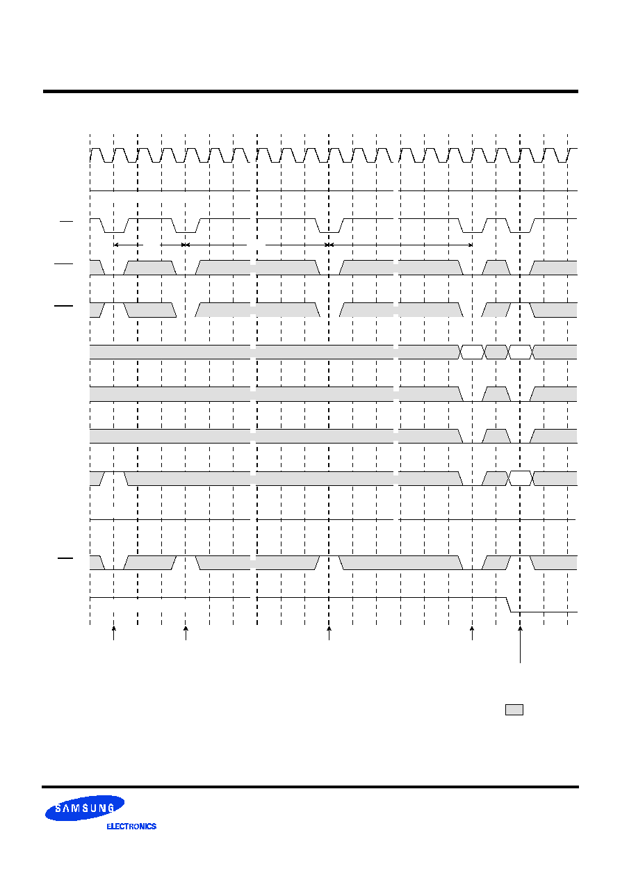
Single Bit Read-Write-Read Cycle(Same Page) @CAS Latency=3, Burst Length=1
: Don't care
tRCD
*Note 1
tSS
tSH
tRP
tCCD
tSS
tSH
tRAC
tSAC
tSLZ
tOH
tSH
tSS
tSS
tSH
tSS
tSH
CLOCK
CKE
CS
RAS
CAS
ADDR
BA
0
~
BA
1
A
10
/AP
DQ
WE
DQM
Row Active
Read
Write
Read
Row Active
Precharge
tCH
tCC
tCL
tRAS
tRC
HIGH
tSH
tSH
tSS
tSS
*Note 2,3
*Note 2,3 *Note 4
*Note 4
*Note 3
*Note 3
*Note 3
Rb
Cc
Cb
Ca
Ra
BS
BS
BS
BS
BS
BS
Ra
Rb
Qc
Db
Qa
*Note 2,3
*Note 2
*Note 2
0 1 2 3 4 5 6 7 8 9 10 11 12 13 14 15 16 17 18 19
CMOS SDRAM
K4S643232C
REV. 1.1 Nov. '99
- 26
*Note : 1. All input expect CKE & DQM can be don't care when CS is high at the CLK high going edge.
2. Bank active & read/write are controlled by BA0~BA1.
3. Enable and disable auto precharge function are controlled by A10/AP in read/write command
BA0
0
0
1
1
0
0
1
1
Operation
Disable auto precharge, leave bank A active at end of burst.
Disable auto precharge, leave bank B active at end of burst.
Disable auto precharge, leave bank C active at end of burst.
Disable auto precharge, leave bank D active at end of burst.
Enable auto precharge, precharge bank A at end of burst.
Enable auto precharge, precharge bank B at end of burst.
Enable auto precharge, precharge bank C at end of burst.
Enable auto precharge, precharge bank D at end of burst.
4. A10/AP and BA0~BA1 control bank precharge when precharge command is asserted.
A10/AP
0
1
BA1
0
1
0
1
0
1
0
1
BA0
0
0
1
1
Active & Read/Write
Bank A
Bank B
Bank C
Bank D
BA1
0
1
0
1
BA0
0
0
1
1
x
Precharge
Bank A
Bank B
Bank C
Bank D
All Banks
A10/AP
0
0
0
0
1
BA1
0
0
1
1
x
0 1 2 3 4 5 6 7 8 9 10 11 12 13 14 15 16 17 18 19
CMOS SDRAM
K4S643232C
REV. 1.1 Nov. '99
- 27
Power Up Sequence
: Don't care
CLOCK
CKE
CS
RAS
CAS
ADDR
BA
0
A
10
/AP
DQ
WE
DQM
Precharge
Auto Refresh
Auto Refresh
Mode Register Set
Row Active
BA
1
RAa
RAa
(All Banks)
(A-Bank)
tRP
tRC
High level is necessary
High-Z
High level is necessary
Key
0 1 2 3 4 5 6 7 8 9 10 11 12 13 14 15 16 17 18 19
CMOS SDRAM
K4S643232C
REV. 1.1 Nov. '99
- 28
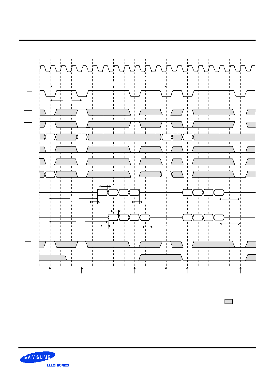
Read & Write Cycle at Same Bank @Burst Length=4
HIGH
: Don't care
*Note :
1. Minimum row cycle times is required to complete internal DRAM operation.
2. Row precharge can interrupt burst on any cycle. [CAS Latency - 1] number of valid output data
is available after Row precharge. Last valid output will be Hi-Z(t
SHZ
) after the clcok.
3. Access time from Row active command. t
CC
*(t
RCD
+ CAS latency - 1) + t
SAC
4. Ouput will be Hi-Z after the end of burst. (1, 2, 4, 8 & Full page bit burst)
5. For -55/60/70/80/10, tRDL=1CLK product can be supported within restricted amounts and it will be distinguished by bucket code
"NV". From the next generation, tRDL will be only 2CLK for every clock frequency
*Note 1
tRC
tRCD
*Note 2
tRDL
tRDL
tSHZ
*Note 4
tSHZ
*Note 4
tOH
tRAC
*Note 3
tSAC
tSAC
tRAC
*Note 3
tOH
BA
0
BA
1
A
10
/AP
CL=2
CL=3
DQ
ADDR
CAS
RAS
CS
CKE
CLOCK
Ra
Rb
Qa0
Qa1
Qa2
Qa3
Qa0
Qa1
Qa2
Qa3
Db0
Db1
Db2
Db3
Db0
Db1
Db2
Db3
Ra
Ca
Rb
Cb
WE
DQM
Row Active
(A-Bank)
Precharge
(A-Bank)
Row Active
(A-Bank)
Write
(A-Bank)
Precharge
(A-Bank)
Read
(A-Bank)
*Note 5
*Note 5
0 1 2 3 4 5 6 7 8 9 10 11 12 13 14 15 16 17 18 19
CMOS SDRAM
K4S643232C
REV. 1.1 Nov. '99
- 29
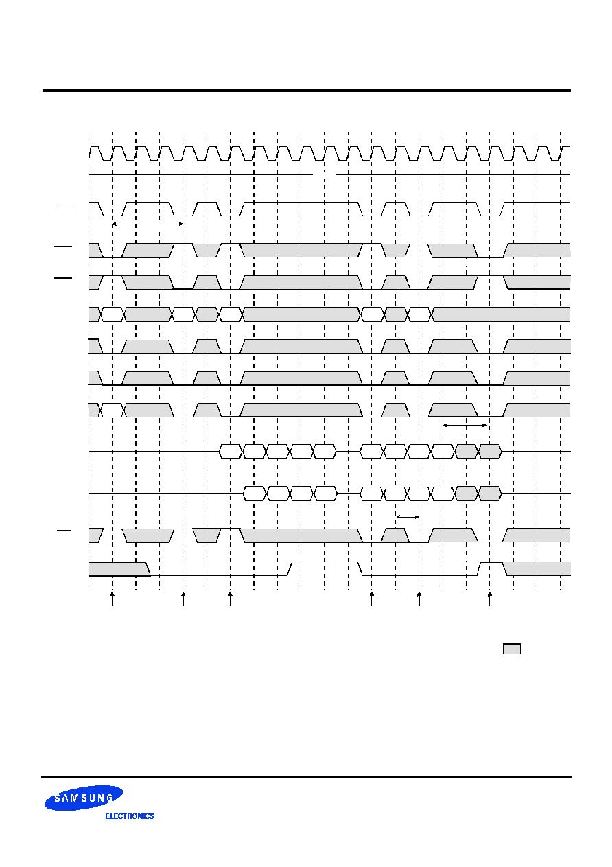
Page Read & Write Cycle at Same Bank @Burst Length=4
HIGH
Row Active
(A-Bank)
Read
(A-Bank)
Write
(A-Bank)
Precharge
(A-Bank)
: Don't care
*Note :
1. To write data before burst read ends, DQM should be asserted three cycle prior to write
command to avoid bus contention.
2. Row precharge will interrupt writing. Last data input, t
RDL
before Row precharge, will be written.
3. DQM should mask invalid input data on precharge command cycle when asserting precharge
before end of burst. Input data after Row precharge cycle will be masked internally.
4. For -55/60/70/80/10, tRDL=1CLK product can be supported within restricted amounts and it will be distinguished by bucket code
"NV". From the next generation, tRDL will be only 2CLK for every clock frequency
Read
(A-Bank)
tRCD
*Note 2
tRDL
*Note 1
*Note 3
tCDL
Qa0
Qa1
Qb0
Qb1
Qb2
Qa0
Qa1
Qb0
Qb1
Dc0
Dc1
Dd0
Dd1
Dc0
Dc1
Dd0
Dd1
Write
(A-Bank)
BA
0
BA
1
A
10
/AP
CL=2
CL=3
DQ
ADDR
CAS
RAS
CS
CKE
CLOCK
WE
DQM
Ra
Ca
Cb
Cc
Cd
Ra
*Note 4

0 1 2 3 4 5 6 7 8 9 10 11 12 13 14 15 16 17 18 19
CMOS SDRAM
K4S643232C
REV. 1.1 Nov. '99
- 30
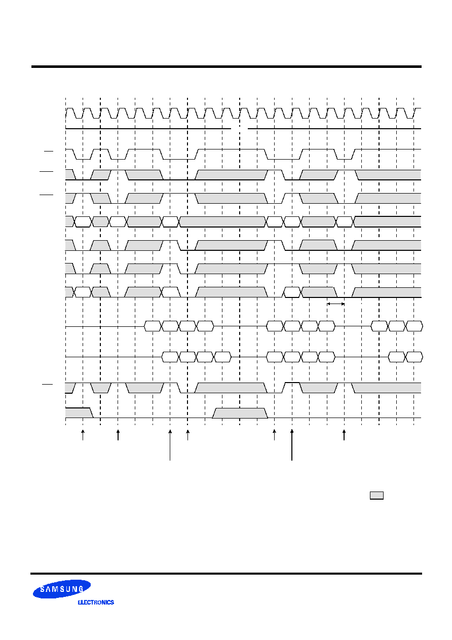
Page Read Cycle at Different Bank @Burst Length=4
HIGH
Row Active
(A-Bank)
Read
(A-Bank)
Read
(C-Bank)
Precharge
(B-Bank)
Read
(D-Bank)
: Don't care
*Note :
1. CS can be don't cared when RAS, CAS and WE are high at the clock high going dege.
2. To interrupt a burst read by row precharge, both the read and the precharge banks must be the same.
Row Active
(B-Bank)
*Note 2
*Note 1
Row Acive
(C-Bank)
Read
(B-Bank)
Precharge
(A-Bank)
Row Active
(D-Bank)
Precharge
(C-Bank)
Precharge
(D-Bank)
BA
0
BA
1
A
10
/AP
CL=2
CL=3
DQ
ADDR
CAS
RAS
CS
CKE
CLOCK
WE
DQM
QAa0
QAa1
QAa2
QBb0
QBb1
QBb2 QCc0
QCc1 QCc2
QDd0 QDd1 QDd2
QAa0 QAa1
QAa2 QBb0
QBb1
QBb2 QCc0
QCc1
QCc2 QDd0 QDd1 QDd2
RAa
RBb
RCc
RDd
RAa
RBb
CAa
RCc
CBb
RDd
CCc
CDd

0 1 2 3 4 5 6 7 8 9 10 11 12 13 14 15 16 17 18 19
CMOS SDRAM
K4S643232C
REV. 1.1 Nov. '99
- 31
Page Write Cycle at Different Bank @Burst Length=4
HIGH
Row Active
(A-Bank)
Write
(A-Bank)
Row Active
(D-Bank)
Write
(D-Bank)
: Don't care
*Note :
1. To interrupt burst write by Row precharge, DQM should be asserted to mask invalid input data.
2. To interrupt burst write by Row precharge, both the write and the precharge banks must be the same.
3.For -55/60/70/80/10, tRDL=1CLK product can be supported within restricted amounts and it will be distinguished by bucket code
"NV". From the next generation, tRDL will be only 2CLK for every clock frequency
Row Active
(B-Bank)
tRDL
Row Active
(C-Bank)
Precharge
(All Banks)
tCDL
Write
(B-Bank)
Write
(C-Bank)
*Note 1
BA
0
BA
1
DQ
ADDR
CAS
RAS
CS
CKE
CLOCK
WE
DQM
A
10
/AP
RAa
RBb
CAa
CBb
RCc
RDd
CCc
CDd
RCc
RDd
RAa
RBb
*Note 2
DAa0
DAa1 DAa2
DAa3
DBb0
DBb1
DBb2 DBb3
DCc0
DCc1
DDd0
DDd1
DDd2
*Note 3
0 1 2 3 4 5 6 7 8 9 10 11 12 13 14 15 16 17 18 19
CMOS SDRAM
K4S643232C
REV. 1.1 Nov. '99
- 32
Read & Write Cycle at Different Bank @Burst Length=4
HIGH
RAa
Row Active
(A-Bank)
Write
(D-Bank)
Precharge
(B-Bank)
: Don't care
*Note :
1. t
CDL
should be met to complete write.
Read
(A-Bank)
RAa
CDb
RBc
*Note 1
tCDL
RDb
CAa
RAc
Row Active
(D-Bank)
Precharge
(A-Bank)
Read
(B-Bank)
CBc
RBb
BA
0
BA
1
A
10
/AP
CL=2
CL=3
DQ
ADDR
CAS
RAS
CS
CKE
CLOCK
WE
DQM
QAa0
QAa1
QAa2
QAa3
QAa0 QAa1
QAa2 QAa3
DDb0
DDb1 DDb2 DDb3
DDb0
DDb1 DDb2 DDb3
QBc0
QBc1
QBc2
QBc0
QBc1
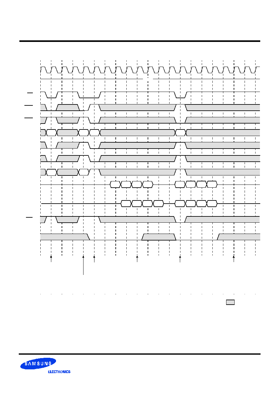
0 1 2 3 4 5 6 7 8 9 10 11 12 13 14 15 16 17 18 19
CMOS SDRAM
K4S643232C
REV. 1.1 Nov. '99
- 33
Read & Write Cycle with Auto Precharge I @Burst Length=4
HIGH
Row Active
(A-Bank)
1.
t
RCD
should be controlled to meet minimum
t
RAS
before internal precharge start.
(In the case of Burst Length=1 & 2, BRSW mode and Block write)
Row Active
(B-Bank)
Read with
Auto Precharge
(A-Bank)
Auto Precharge
Start Point
(B-Bank)
Auto Precharge
Start Point
(A-Bank)
Write with
Auto Precharge
(B-Bank)
ADDR
CAS
RAS
CS
CKE
CLOCK
WE
DQM
RAa
RBb
CAa
RBb
CBb
*Note :
: Don
t care
(CL=2)
(CL=3)
DQ
DQ
RAa
QAa0
QAa1
QAa2
QAa3
QAa0 QAa1
QAa2 QAa3
DBb0
DBb1
DBb2 DBb3
DBb0
DBb1
DBb2 DBb3
BA
0
A
10
/AP
BA
1
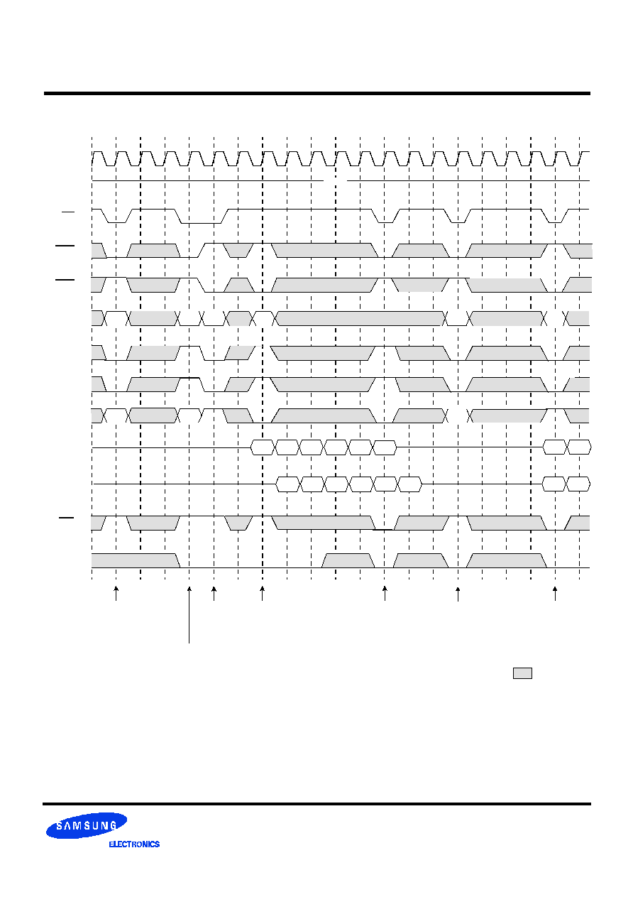
0 1 2 3 4 5 6 7 8 9 10 11 12 13 14 15 16 17 18 19
CMOS SDRAM
K4S643232C
REV. 1.1 Nov. '99
- 34
Read & Write Cycle with Auto Precharge II @Burst Length=4
HIGH
Row Active
(A-Bank)
: Don't care
*Note:
* When Read(Write) command with auto precharge is issued at A-Bank after A and B Bank activation.
- if Read(Write) command without auto precharge is issued at B-Bank before A Bank auto precharge starts, A Bank
auto precharge will start at B Bank read command input point .
- any command can not be issued at A Bank during tRP after A Bank auto precharge starts.
Row Active
(B-Bank)
Read with
Auto Pre
charge
(A-Bank)
Write with
Auto Precharge
(A-Bank)
Row Active
(A-Bank)
BA
0
A
10
/AP
CL=2
CL=3
DQ
ADDR
CAS
RAS
CS
CKE
CLOCK
WE
DQM
Qa0
Qa1
Qb0
Qb1
Qa0
Qa1
Qb0
Qb1
Ra
Rb
Ca
Ra
Rb
Ra
Cb
Qb2
Qb3
Read without Auto
precharge(B-Bank)
Auto Precharge
Start Point
(A-Bank)*
Precharge
(B-Bank)
Da0
Da1
Da0
Da1
Qb2
Qb3
Ca
Ra
BA
1
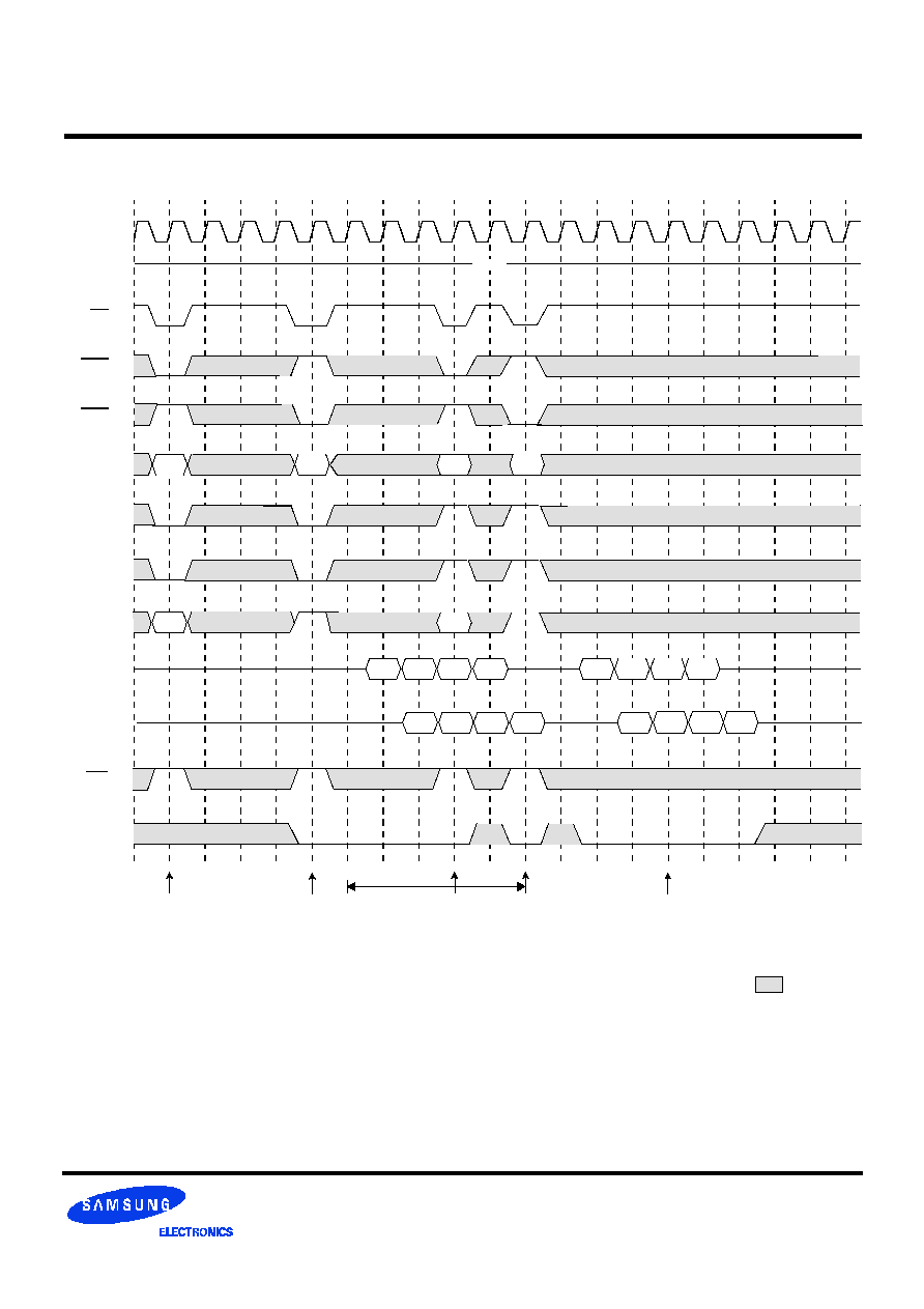
0 1 2 3 4 5 6 7 8 9 10 11 12 13 14 15 16 17 18 19
CMOS SDRAM
K4S643232C
REV. 1.1 Nov. '99
- 35
Read & Write Cycle with Auto Precharge III @Burst Length=4
HIGH
Row Active
(A-Bank)
: Don't care
*Note :
* Any command to A-bank is not allowed in this period.
tRP is determined from at auto precharge start point
Read with
Auto Precharge
(A-Bank)
Auto Precharge
Start Point
(A-Bank)
Row Active
(B-Bank)
Read with
Auto Precharge
(B-Bank)
BA
0
A
10
/AP
CL=2
CL=3
DQ
ADDR
CAS
RAS
CS
CKE
CLOCK
WE
DQM
Qa0
Qa1
Qa2
Qa3
Qa0
Qa1
Qa2
Qa3
Qb0
Qb1
Qb2
Qb3
Qb0
Qb1
Qb2
Qb3
Ra
Ca
Ra
Cb
Rb
Rb
*
Auto Precharge
Start Point
(B-Bank)
BA
1
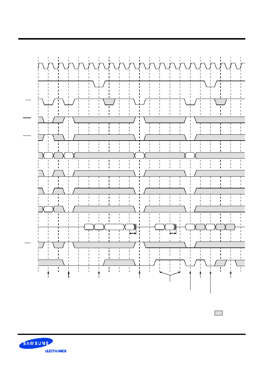
0 1 2 3 4 5 6 7 8 9 10 11 12 13 14 15 16 17 18 19
CMOS SDRAM
K4S643232C
REV. 1.1 Nov. '99
- 36
Clock Suspension & DQM Operation Cycle @CAS Latency=2, Burst Length=4
Ra
Row Active
Clock
Suspension
Read
Write
DQM
: Don't care
Clock
Suspension
Read
*Note 1
tSHZ
tSHZ
Write
DQM
Write
Read DQM
*Note :
1. DQM is needed to prevent bus contention.
BA
0
BA
1
DQ
ADDR
CAS
RAS
CS
CKE
CLOCK
WE
DQM
A
10
/AP
Ra
Ca
Cb
Cc
Dc2
Dc0
Qb1
Qb0
Qa3
Qa2
Qa1
Qa0
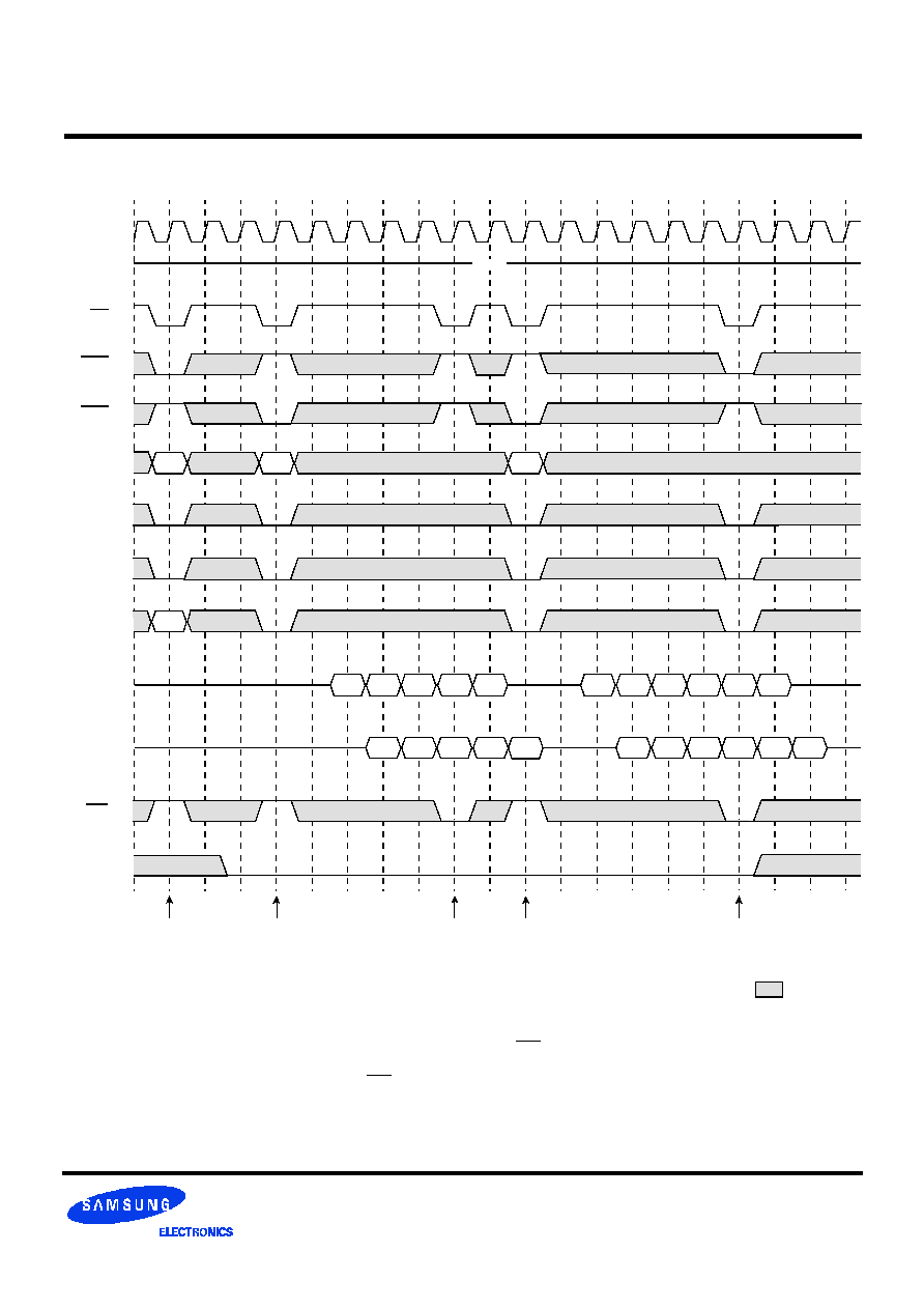
0 1 2 3 4 5 6 7 8 9 10 11 12 13 14 15 16 17 18 19
CMOS SDRAM
K4S643232C
REV. 1.1 Nov. '99
- 37
Read Interrupted by Precharge Command & Read Burst Stop Cycle @Burst Length=Full page
HIGH
Row Active
(A-Bank)
: Don't care
*Note :
1. At full page mode, burst is wrap-around at the end of burst. So auto precharge is impossible.
2. About the valid DQs after burst stop, it is same as the case of RAS interrupt.
Both cases are illustrated above timing diagram. See the label 1, 2 on them.
But at burst write, Burst stop and RAS interrupt should be compared carefully.
Refer the timing diagram of "Full page write burst stop cycle".
3. Burst stop is valid at every burst length.
Precharge
(A-Bank)
Burst Stop
Read
(A-Bank)
Read
(A-Bank)
1
2
1
2
BA
0
BA
1
A
10
/AP
CL=2
CL=3
DQ
ADDR
CAS
RAS
CS
CKE
CLOCK
WE
DQM
QAa0
QAa1 QAa2
QAa3 QAa4
QAa0 QAa1 QAa2 QAa3 QAa4
QAb0
QAb1 QAb2
QAb3 QAb4 QAb5
QAb0 QAb1 QAb2 QAb3
QAb4 QAb5
RAa
CAa
CAb
RAa
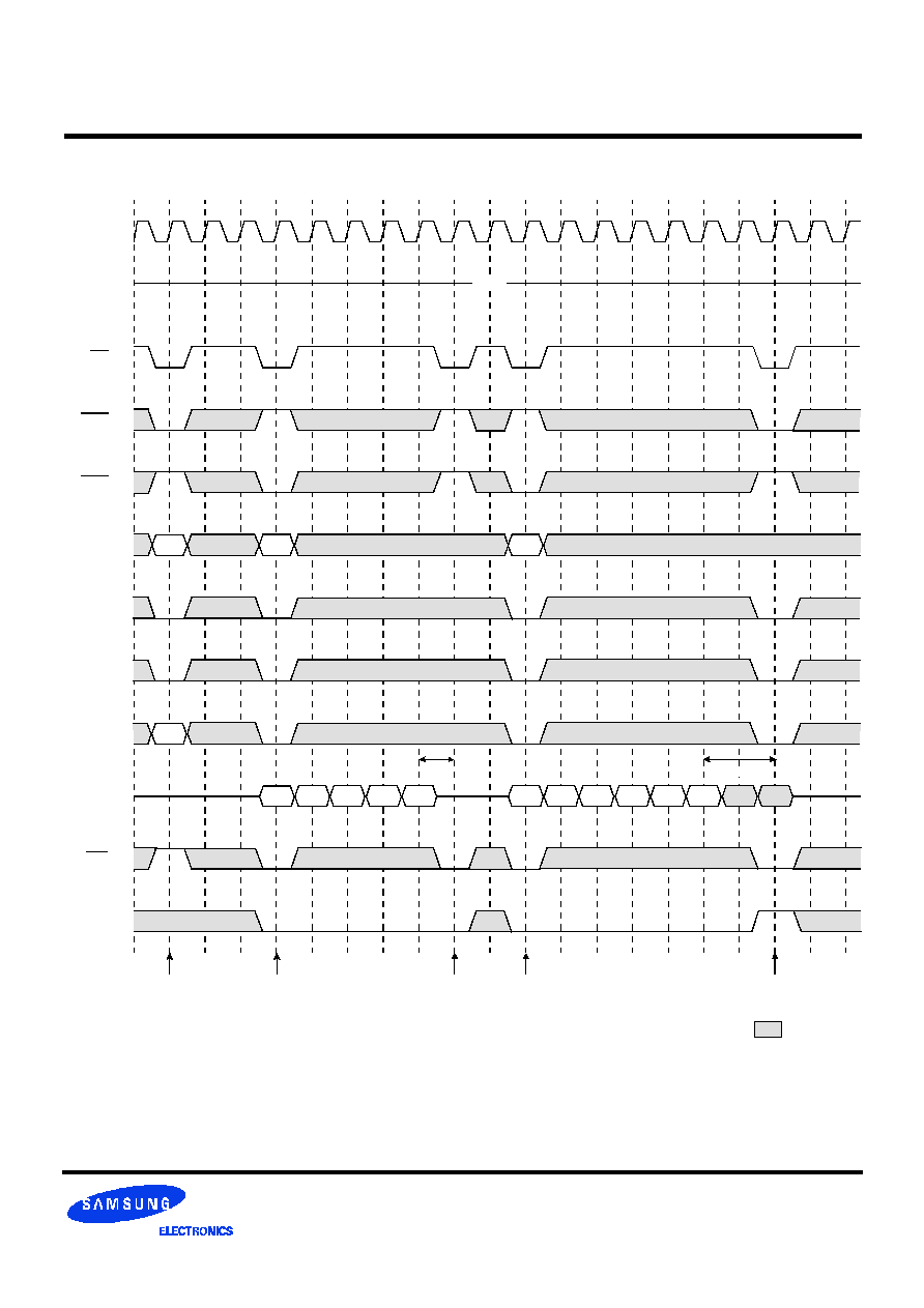
0 1 2 3 4 5 6 7 8 9 10 11 12 13 14 15 16 17 18 19
CMOS SDRAM
K4S643232C
REV. 1.1 Nov. '99
- 38
Write Interrupted by Precharge Command & Write Burst Stop Cycle @ Burst Length=Full page
Row Active
(A-Bank)
Burst Stop
Write
(A-Bank)
Precharge
(A-Bank)
: Don't care
Write
(A-Bank)
*Note 2,4
tBDL
*Note :
1. At full page mode, burst is wrap-around at the end of burst. So auto precharge is impossible.
2. Data-in at the cycle of interrupted by precharge can not be written into the corresponding memory cell. It is defined by AC
parameter of t
RDL.
DQM at write interrupted by precharge command is needed to prevent invalid write.
DQM should mask invalid input data on precharge command cycle when asserting precharge before end of burst.
Input data after Row precharge cycle will be masked internally.
3. Burst stop is valid at every burst length.
4. For -55/60/70/80/10, tRDL=1CLK product can be supported within restricted amounts and it will be distinguished by bucket code
"NV". From the next generation, tRDL will be only 2CLK for every clock frequency.
HIGH
tRDL
BA
0
BA
1
DQ
ADDR
CAS
RAS
CS
CKE
CLOCK
WE
DQM
A
10
/AP
DAa0
DAa1
DAa2
DAa3 DAa4
DAb0
DAb1
DAb2
DAb3 DAb4
DAb5
RAa
CAa
CAb
RAa
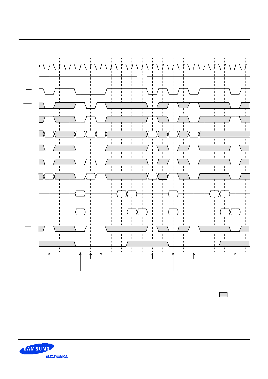
0 1 2 3 4 5 6 7 8 9 10 11 12 13 14 15 16 17 18 19
CMOS SDRAM
K4S643232C
REV. 1.1 Nov. '99
- 39
Burst Read Single bit Write Cycle @Burst Length=2
HIGH
Row Active
(A-Bank)
Row Active
(C-Bank)
Write with
Auto Precharge
(B-Bank)
: Don't care
*Note :
1. BRSW modes is enabled by setting A
9
"High" at MRS (Mode Register Set).
At the BRSW Mode, the burst length at write is fixed to "1" regardless of programmed burst length.
2. When BRSW write command with auto precharge is executed, keep it in mind that t
RAS
should not be violated.
Auto precharge is executed at the burst-end cycle, so in the case of BRSW write command,
the next cycle starts the precharge.
Write
(A-Bank)
*Note 1
Row Active
(B-Bank)
Read
(C-Bank)
Read with
Auto Precharge
(A-Bank)
Precharge
(C-Bank)
*Note 2
BA
0
BA
1
A
10
/AP
CL=2
CL=3
DQ
ADDR
CAS
RAS
CS
CKE
CLOCK
WE
DQM
DAa0
DAa0
QAb0
QAb1
QAb0
QAb1
DBc0
DBc0
QCd0
QCd1
QCd0
QCd1
RAa
CAa
RBb
CAb
RCc
CBc
CCd
RAc
RAa
RBb

0 1 2 3 4 5 6 7 8 9 10 11 12 13 14 15 16 17 18 19
CMOS SDRAM
K4S643232C
REV. 1.1 Nov. '99
- 40
Active/Precharge Power Down Mode @CAS Latency=2, Burst Length=4
Precharge
Power-down
Entry
: Don
°«
t Care
*Note :
1. Both banks should be in idle state prior to entering precharge power down mode.
2. CKE should be set high at least 1CLK + tss prior to Row active command.
3. Can not violate minimum refresh specification. (64ms)
*Note 1
Precharge
tSS
*Note 2
BA
DQ
ADDR
CAS
RAS
CS
CKE
CLOCK
WE
DQM
A
10
/AP
tSS
tSS
Ra
Ca
Ra
Qa0
Qa1
Qa2
Row Active
Precharge
Power-down
Exit
Active
Power-down
Entry
Active
Power-down
Exit
Read
tSHZ
*Note 3
*Note 2

0 1 2 3 4 5 6 7 8 9 10 11 12 13 14 15 16 17 18 19
CMOS SDRAM
K4S643232C
REV. 1.1 Nov. '99
- 41
Self Refresh Entry & Exit Cycle
Self Refresh Entry
: Don't care
*Note :
TO ENTER SELF REFRESH MODE
1. CS, RAS & CAS with CKE should be low at the same clcok cycle.
2. After 1 clock cycle, all the inputs including the system clock can be don't care except for CKE.
3. The device remains in self refresh mode as long as CKE stays
"Low".
cf.) Once the device enters self refresh mode, minimum t
RAS
is required before exit from self refresh.
TO EXIT SELF REFRESH MODE
4. System colck restart and be stable before returning CKE high.
5. CS starts from high.
6. Minimum t
RFC
is required after CKE going high to complete self refresh exit.
7. 4K cycle of burst auto refresh is required before self refresh entry and after self refresh exit if the system uses burst refresh.
*Note 1
*Note 7
Hi-Z
Hi-Z
Self Refresh Exit
Auto Refresh
tSS
*Note 2
*Note 3
*Note 4
tRFCmin
*Note 6
*Note 5
BA
0
~BA
1
DQ
ADDR
CAS
RAS
CS
CKE
CLOCK
WE
DQM
A
10
/AP
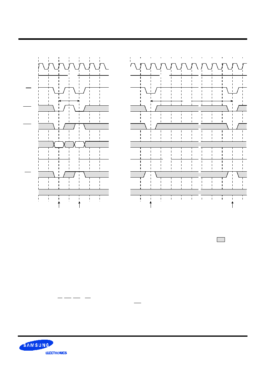
0 1 2 3 4 5 6 7 8 9 10 11 12 13 14 15 16 17 18 19
CMOS SDRAM
K4S643232C
REV. 1.1 Nov. '99
- 42
Mode Register Set Cycle
HIGH
MRS
Auto Refresh
: Don't care
*Note :
1. CS, RAS, CAS, & WE activation at the same clock cycle with address key will set internal mode register.
2. Minimum 2 clock cycles should be met before new RAS activation.
3. Please refer to Mode Register Set table.
New
Command
New Command
Hi-Z
Hi-Z
°Û
°Û
tRFC
HIGH
MODE REGISTER SET CYCLE
* All banks precharge should be completed before Mode Register Set cycle and auto refresh cycle.
Auto Refresh Cycle
0 1 2 3 4 5 6 7 8 9 10
DQ
ADDR
CAS
RAS
CS
CKE
CLOCK
WE
DQM
Key
Ra
*Note 3
*Note 1
*Note 2
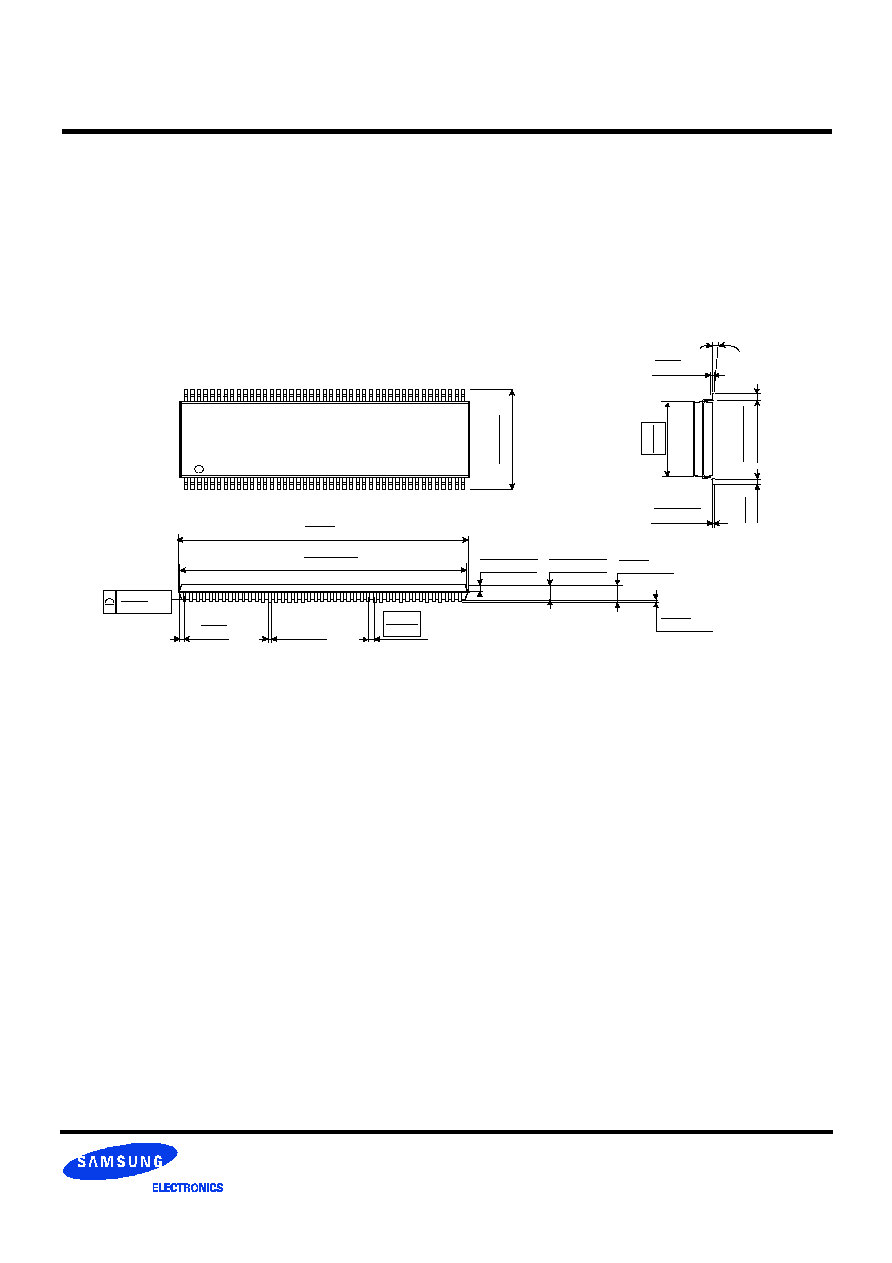
K4S643232C
CMOS SDRAM
REV. 1.1 Nov. '99
- 43
#1
1
1
.
7
6
±
0
.
2
0
0
.
4
6
3
±
0
.
0
0
8
0
.
0
2
0
0
.
5
0
(
)
0.005
-0.001
+0.003
0.125
-0.035
+0.075
0
.
4
0
0
1
0
.
1
6
0
.
4
5
~
0
.
7
5
0
.
0
1
8
~
0
.
0
3
0
0.010
0.25
TYP
0~8
∞
C
#86
#44
#43
0.010
0.05
MIN
0.008
0.21
±
0.002
±
0.05
0.004
0.10
MAX
0.024
0.61
( )
0.0197
0.50
0.047
1.20
MAX
0.039
1.00
±
0.004
±
0.10
0.891
22.62
MAX
0.875
22.22
±
0.004
±
0.10
0.20
+0.10
-0.03
86-TSOP2-400F
Unit : Millimeters
PACKAGE DIMENSIONS