Page 2 of 29
1Gb M-die DDR2 SDRAM
Rev.1.1 Jan. 2005
DDR2 SDRAM
Contents
0. Ordering Information
1. Key Feature
2. Package Pinout/Mechnical Dimension & Addressing
2.1 Package Pintout & Mechnical Dimension
2.2 Input/Output Function Description
2.3 Addressing
3. Absolute Maximum Rating
4. AC & DC Operating Conditions & Specifications
Page 3 of 29
1Gb M-die DDR2 SDRAM
Rev.1.1 Jan. 2005
DDR2 SDRAM
1.Key Features
Note : This data sheet is an abstract of full DDR2 specification and does not cover the common features
which are described in "DDR2 SDRAM Device Operation & Timing Diagram".
Speed
DDR2-533
4-4-4
DDR2-400
3-3-3
Units
CAS Latency
4
3
tCK
tRCD(min)
15
15
ns
tRP(min)
15
15
ns
tRC(min)
55
55
ns
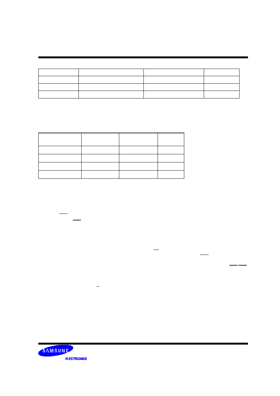
0. Ordering Information
Note : Speed bin is in order of CL-tRCD-tRP
Organization
DDR2-533 4-4-4
DDR2-400 3-3-3
Package
256Mx4
K4T1G044QM-ZCD5
K4T1G044QM-ZCCC
Lead-Free
128Mx8
K4T1G084QM-ZCD5
K4T1G084QM-ZCCC
Lead-Free
64Mx16
K4T1G164QM-ZCD5
K4T1G164QM-ZCCC
Lead-Free
� JEDEC standard 1.8V � 0.1V Power Supply
� VDDQ = 1.8V � 0.1V
� 200 MHz f
CK
for 400Mb/sec/pin, 267MHz f
CK
for
533Mb/sec/pin.
� 8 Banks
� Posted CAS
� Programmable CAS Latency: 3, 4, 5
� Programmable Additive Latency: 0, 1 , 2 , 3 and 4
� Write Latency(WL) = Read Latency(RL) -1
� Burst Length: 4 , 8(Interleave/nibble sequential)
� Programmable Sequential / Interleave Burst Mode
� Bi-directional Differential Data-Strobe (Single-ended
data-strobe is an optional feature)
� Off-Chip Driver(OCD) Impedance Adjustment
� On Die Termination
� Average Refresh Period 7.8us at lower than T
CASE
85
�
C, 3.9us at 85
�
C < T
CASE
< 95
�
C
� Package: 68ball FBGA - 256Mx4/128Mx8 , 92ball
FBGA - 64Mx16
� All of Lead-free products are compliant for RoHS
The 1Gb DDR2 SDRAM is organized as a 32Mbit x 4 I/Os
x 8 banks, 16Mbit x 8 I/Os x 8banks or 8Mbit x 16 I/Os x 8
banks device. This synchronous device achieves high
speed double-data-rate transfer rates of up to
533Mb/sec/pin (DDR2-533) for general applications.
The chip is designed to comply with the following key
DDR2 SDRAM features such as posted CAS with additive
latency, write latency = read latency - 1, Off-Chip
Driver(OCD) impedance adjustment and On Die Termina-
tion.
All of the control and address inputs are synchronized with
a pair of externally supplied differential clocks. Inputs are
latched at the crosspoint of differential clocks (CK rising
and CK falling). All I/Os are synchronized with a pair of
bidirectional strobes (DQS and DQS) in a source synchro-
nous fashion. The address bus is used to convey row, col-
umn, and bank address information in a RAS/CAS
multiplexing style. For example, 1Gb(x4) device receive
14/11/3 addressing.
The 1Gb DDR2 device operates with a single 1.8V � 0.1V
power supply and 1.8V � 0.1V VDDQ.
The 1Gb DDR2 device is available in 68ball FBGAs(x4/x8)
and in 92ball FBGAs(x16).
Note: The functionality described and the timing specifica-
tions included in this data sheet are for the DLL Enabled
mode of operation.
Page 4 of 29
1Gb M-die DDR2 SDRAM
Rev.1.1 Jan. 2005
DDR2 SDRAM
2. Package Pinout/Mechnical Dimension & Addressing
2.1 Package Pinout
Notes:
1. Pin E3 has identical
capacitance as pin E7.
2. VDDL and VSSDL are
power and ground for the
DLL.
x4 package pinout (Top View) : 68ball FBGA Package
(60balls + 8balls of dummy balls)
A
B
C
D
E
F
G
H
J
K
L
VDD
NC
VSS
NC
VSSQ
DM
VDDQ
VDDQ
VDDQ
VSSQ
VSSQ
DQS
DQS
NC
DQ0
VDDQ
DQ2
VSSQ
NC
VSSDL
VDD
CK
RAS
CK
CAS
CS
A2
A6
A4
A11
A8
NC
A13
NC
A12
A9
A7
A5
A0
VDD
A10/AP
VSS
VDDQ
VSSQ
DQ1
DQ3
NC
VDDL
A1
A3
BA1
VREF
VSS
CKE
WE
BA0
1 2 3 7 8 9
VDD
VSS
ODT
BA2
Ball Locations (x4)
: Populated Ball
+ : Depopulated Ball
Top View (See the balls through the Package)
NC
NC
NC
NC
M
N
P
R
T
U
V
W
NC
NC
NC
NC
+
+
+
+
+
+
+
+
+
+
+
+
+
+
+
+
+
+
+
+
+
+
+
+
+
+
+
+
+
+
1
2
3
4
5
6
7
8
9
A
B
C
D
E
F
G
H
J
K
L
+
+
+
+
+
+
+
+
+
+
+
+
+
+
+
+
+
+
+
+
+
+
+
+
+
+
+
+
+
+
+
+
+
+
+
+
+
+
+
+
+
+
+
+
+
+
+
+
+
+
+
+
+
+
+
+
+
+
+
+
+
+ + +
+
+
+ + +
+ + +
M
N
P
R
T
U
V
W
+
Page 5 of 29
1Gb M-die DDR2 SDRAM
Rev.1.1 Jan. 2005
DDR2 SDRAM
Notes:
1.
Pins F3 and E2 have
identical capacitance as
pins F7 and E8.
2.
For a read, when enabled,
strobe pair RDQS &
RDQS are identical in
function and timing to
strobe pair DQS & DQS
and input masking
function is disabled.
3.
The function of DM or
RDQS/RDQS are enabled
by EMRS command.
4.
VDDL and VSSDL are
power and ground for the
DLL.
x8 package pinout (Top View) : 68ball FBGA Package
(60balls + 8balls of dummy balls)
A
B
C
D
E
F
G
H
J
K
L
VDD
NU/
VSS
DQ6
VSSQ
VDDQ
VDDQ
VDDQ
VSSQ
VSSQ
DQS
DQS
DQ7
DQ0
VDDQ
DQ2
VSSQ
DQ5
VSSDL
VDD
CK
RAS
CK
CAS
CS
A2
A6
A4
A11
A8
NC
A13
NC
A12
A9
A7
A5
A0
VDD
A10/AP
VSS
VDDQ
VSSQ
DQ1
DQ3
DQ4
VDDL
A1
A3
BA1
VREF
VSS
CKE
WE
BA0
1 2 3 7 8 9
VDD
VSS
ODT
BA2
NC
NC
NC
NC
M
N
P
R
T
U
V
W
NC
NC
NC
NC
Ball Locations (x8)
: Populated Ball
+ : Depopulated Ball
Top View (See the balls through the Package)
+
+
+
+
+
+
+
+
+
+
+
+
+
+
+
+
+
+
+
+
+
+
+
+
+
+
+
+
+
+
1
2
3
4
5
6
7
8
9
A
B
C
D
E
F
G
H
J
K
L
+
+
+
+
+
+
+
+
+
+
+
+
+
+
+
+
+
+
+
+
+
+
+
+
+
+
+
+
+
+
+
+
+
+
+
+
+
+
+
+
+
+
+
+
+
+
+
+
+
+
+
+
+
+
+
+
+
+
+
+
+
+ + +
+
+
+ + +
+ + +
M
N
P
R
T
U
V
W
DM/
RDQS
RDQS
+