Page 1 of 38
512Mb B-die DDR2 SDRAM
Rev. 0.91 (Sep. 2003)
DDR2 SDRAM
Preliminary
512Mb B-die DDR2 SDRAM Specification
Version 0.91
September 2003

Page 2 of 38
512Mb B-die DDR2 SDRAM
Rev. 0.91 (Sep. 2003)
DDR2 SDRAM
Preliminary
Contents
1. Key Feature
2. Package Pinout/Mechnical Dimension & Addressing
2.1 Package Pintout & Mechnical Dimension
2.2 Input/Output Function Description
2.3 Addressing
3. Command Truth Table
3.1 Command truth table
3.2 Clock Enable (CKE) Truth Table for Synchronous Transitions
3.3 DM Truth Table
4. Absolute Maximum Rating
5. AC & DC Operating Conditions & Specifications

Page 3 of 38
512Mb B-die DDR2 SDRAM
Rev. 0.91 (Sep. 2003)
DDR2 SDRAM
Preliminary
Revision History
Version 0.9 (Aug. 2003)
- Initial Release
Version 0.91 (Sep. 2003)
- Corrected from M to B in Part No Information(K4T51##3Q"M"-### -> K4T51##3Q"B"-###)
- Removed D4 speed bin(400 4-4-4)
- Added operation temperature condition
- Changed setup/hold time values(tlS/tDS, tIH/tDH)
- Added notes for setup/hold time(tIS/tDS, tIH/tDH)
- Changed in/output capacitance values
- Added tREFI values by T
CASE
(85
∞
C/95
∞
C)
Page 4 of 38
512Mb B-die DDR2 SDRAM
Rev. 0.91 (Sep. 2003)
DDR2 SDRAM
Preliminary
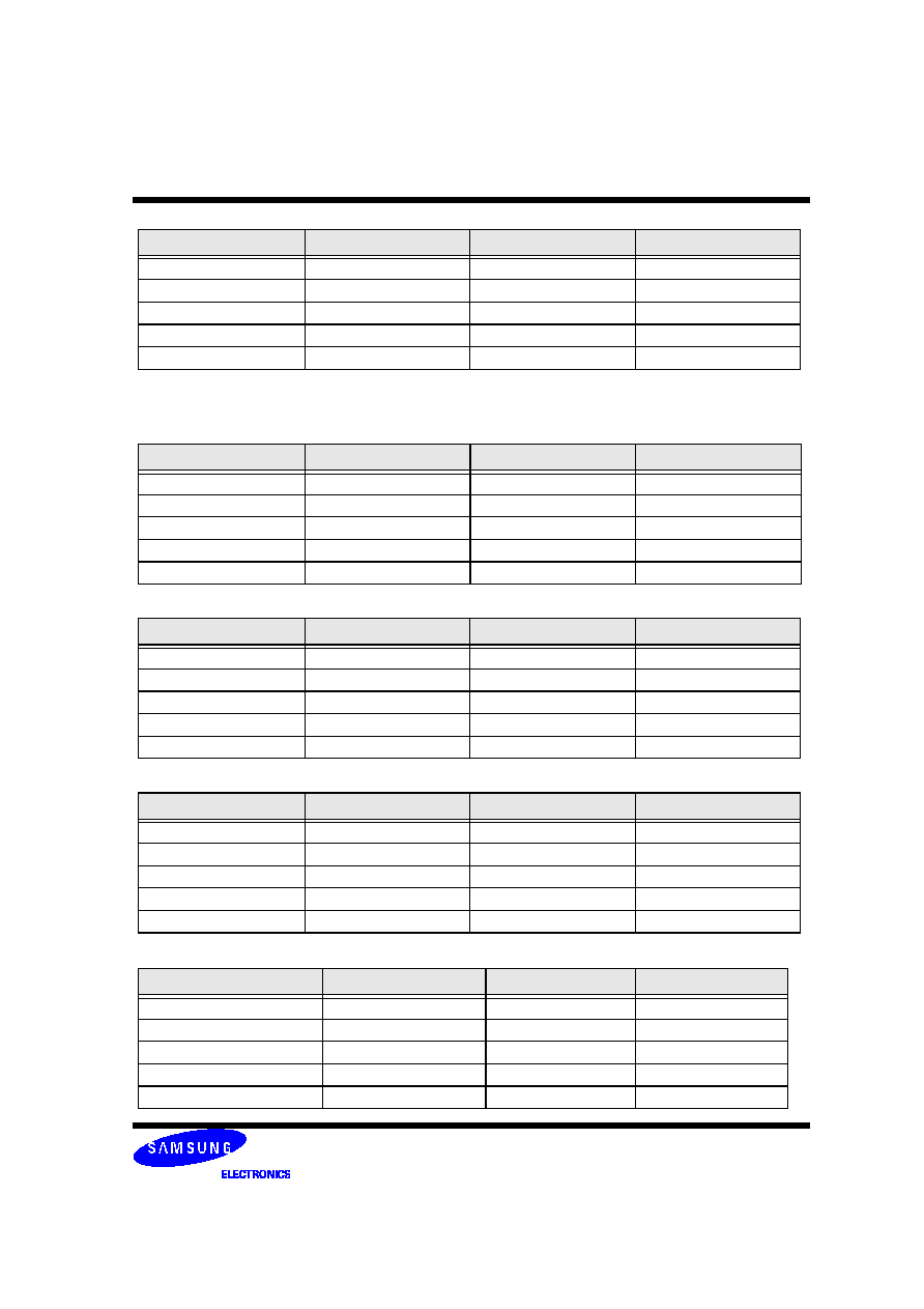
Part Number Information
Note:
1. Speed bin is in order of CL-tRCD-tRP
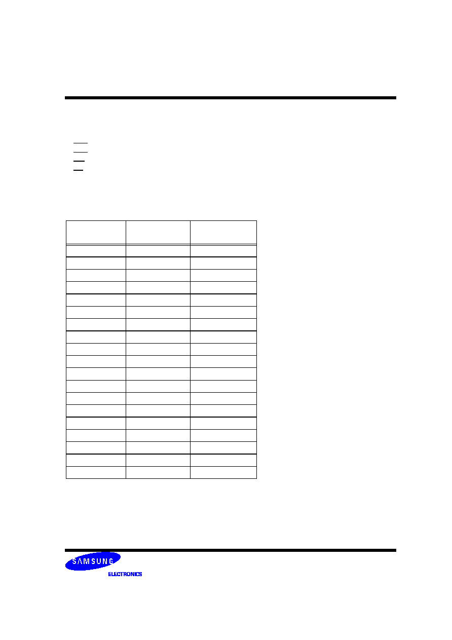
Organization
DDR2-667 5-5-5
DDR2-533 4-4-4
DDR2-400 3-3-3
128Mx4
K4T51043QB-GCE6
K4T51043QB-GCD5
K4T51043QB-GCCC
K4T51043QB-GLE6
K4T51043QB-GLD5
K4T51043QB-GLCC
64Mx8
K4T51083QB-GCE6
K4T51083QB-GCD5
K4T51083QB-GCCC
K4T51083QB-GLE6
K4T51083QB-GLD5
K4T51083QB-GLCC
32Mx16
K4T51163QB-GCE6
K4T51163QB-GCD5
K4T51163QB-GCCC
K4T51163QB-GLE6
K4T51163QB-GLD5
K4T51163QB-GLCC
G : BGA
CC : DDR2-400 3-3-3
D5 : DDR2-533 4-4-4
E6 : DDR2-667 5-5-5
C : (Commercial, Normal)
L : (Commercial, Low)
04 : x4
08 : x8
16 : x16
51 : 512M 8K/64ms
T : DDR2 SDRAM
M : 1st Generation
A : 2nd Generation
B : 3rd Generation
C : 4th Generation
D : 5th Generation
E : 6th Generation
K 4 T XX XX X X X - X X
Memory
DRAM
Small Classification
Density and Refresh
Temperature & Power
Package
Organization
Version
Interface (VDD & VDDQ)
1. SAMSUNG Memory : K
2. DRAM : 4
3. Small Classification
4. Density & Refresh
5. Organization
8. Version
9. Package
10. Temperature & Power
11. Speed
3 : 4 Bank
6. Bank
1 2 3 4 5 6 7 8 9 10 11
XX
Q: SSTL-18(1.8V, 1.8V)
7. Interface (VDD & VDDQ)
Speed
Bank
Page 5 of 38
512Mb B-die DDR2 SDRAM
Rev. 0.91 (Sep. 2003)
DDR2 SDRAM
Preliminary
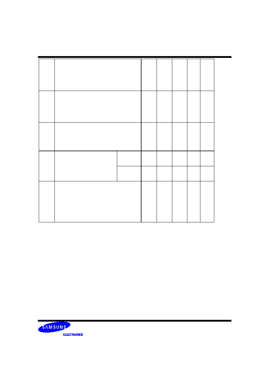
1.Key Features
∑ JEDEC standard 1.8V ± 0.1V Power Supply
∑ VDDQ = 1.8V ± 0.1V
∑ 200 MHz f
CK
for 400Mb/sec/pin, 267MHz f
CK
for 533Mb/sec/pin, 333MHz f
CK
for 667Mb/sec/pin
∑ 4 Bank
∑ Posted CAS
∑ Programmable CAS Latency: 3, 4, 5
∑ Programmable Additive Latency: 0, 1 , 2 , 3 and 4
∑ Write Latency(WL) = Read Latency(RL) -1
∑ Burst Length: 4 , 8(Interleave/nibble sequential)
∑ Programmable Sequential / Interleave Burst Mode
∑ Bi-directional Differential Data-Strobe (Single-ended data-strobe is an optional feature)
∑ Off-Chip Driver(OCD) Impedance Adjustment
∑ On Die Termination
∑ Average Refesh Period 7.8us at lower then T
CASE
85
∞
C, 3.9us at 85
∞
C < T
CASE
< 95
∞
C
∑ Package: 60ball FBGA - 128Mx4/64Mx8 , 84ball FBGA - 32Mx16
Speed
DDR2-667
5 - 5- 5
DDR2-533
4 - 4 - 4
DDR2-400
3- 3- 3
Units
CAS Latency
5
4
3
tCK
tRCD(min)
15
15
15
ns
tRP(min)
15
15
15
ns
tRC(min)
55
55
55
ns
Page 6 of 38
512Mb B-die DDR2 SDRAM
Rev. 0.91 (Sep. 2003)
DDR2 SDRAM
Preliminary
Description
The 512Mb DDR2 SDRAM chip is organized as either 32Mbit x 4 I/O x 4 banks or 16Mbit x 8 I/O x 4banks or
8Mbit x 16I/O x 4 banks device. This synchronous device achieve high speed double-data-rate transfer rates
of up to 667Mb/sec/pin (DDR2-667) for general applications.
The chip is designed to comply with the following key DDR2 SDRAM features: (1) posted CAS with additive
latency, (2) write latency = read latency -1, (3) Off-Chip Driver(OCD) impedance adjustment, (4) On Die Ter-
mination.
All of the control and address inputs are synchronized with a pair of externally supplied differential clocks.
Inputs are latched at the cross point of differential clocks (CK rising and CK falling). All I/Os are synchronized
with a pair of bidirectional strobes (DQS and DQS) in a source synchronous fashion. A fourteen bit address
bus is used to convey row, column, and bank address information in a RAS/CAS multiplexing style. For
example, 512Mb(x4) device receive 14/11/2 addressing.
The 512Mb DDR2 devices operate with a single 1.8V ± 0.1V power supply and 1.8V ± 0.1V VDDQ.
The 512Mb DDR2 devices are available in 60ball FBGAs(x4/8) and in 84ball FBGAs(x16).
Note: The functionality described and the timing specifications included in this data sheet are for the DLL
Enabled mode of operation.

Page 7 of 38
512Mb B-die DDR2 SDRAM
Rev. 0.91 (Sep. 2003)
DDR2 SDRAM
Preliminary
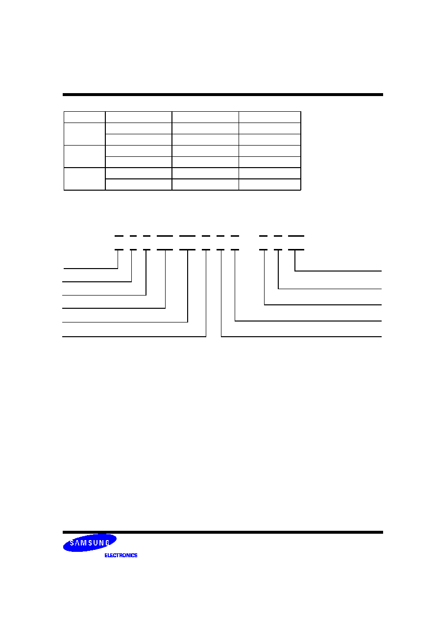
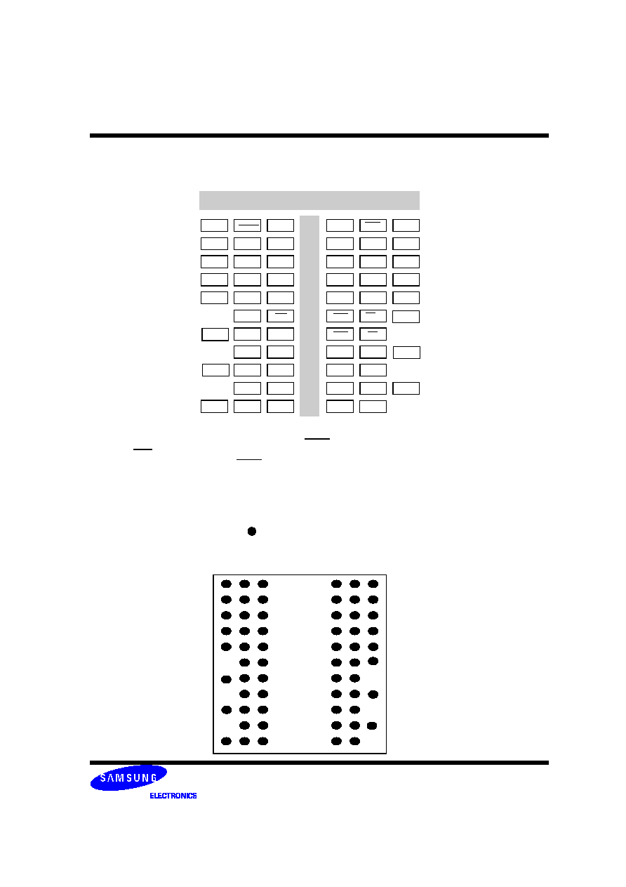
2. Package Pinout/Mechnical Dimension & Addressing
2.1 Package Pinout
x4 package pinout (Top View) : 60ball FBGA Package
Notes:
B1, B9, D1, D9 = NC for x4 organization.
Pins B3 has identical capacitance as pins B7.
VDDL and VSSDL are power and ground for the DLL. It is recommended that they are isolated on the device from
VDD, VDDQ, VSS, and VSSQ.
A
B
C
D
E
F
G
H
J
K
L
VDD
NC
VSS
NC
VSSQ
DM
VDDQ
VDDQ
VDDQ
VSSQ
VSSQ
DQS
DQS
NC
DQ0
VDDQ
DQ2
VSSQ
NC
VSSDL
VDD
CK
RAS
CK
CAS
CS
A2
A6
A4
A11
A8
NC
A13
NC
A12
A9
A7
A5
A0
VDD
A10
VSS
VDDQ
VSSQ
DQ1
DQ3
NC
VDDL
A1
A3
BA1
VREF
VSS
CKE
WE
BA0
1 2 3 7 8 9
VDD
VSS
ODT
NC
+
+
+
+
+
+
+
+
+
+
+
+
+
+
+
+
+
+
+
+
+
+
+
+
+
+
+
+
+
+
+
+
+
+
+
+
+
+
+
+
1
2
3
4
5
6
7
8
9
A
B
C
D
E
F
G
H
J
K
L
Ball Locations (x4)
: Populated Ball
+ : Depopulated Ball
Top View (See the balls through the Package)
Page 8 of 38
512Mb B-die DDR2 SDRAM
Rev. 0.91 (Sep. 2003)
DDR2 SDRAM
Preliminary
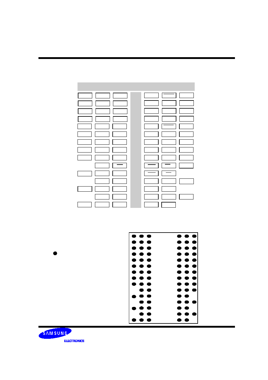
Notes:
1.
Pins B3 and A2 have identical capacitance as pins B7 and A8.
2.
For a read, when enabled, strobe pair RDQS & RDQS are identical in function and timing to strobe pair DQS
& DQS and input masking function is disabled.
3.
The function of DM or RDQS/RDQS are enabled by EMRS command.
4.
VDDL and VSSDL are power and ground for the DLL. It is recommended that they are isolated on the device
from VDD, VDDQ, VSS, and VSSQ.
x8 package pinout (Top View) : 60ball FBGA Package
A
B
C
D
E
F
G
H
J
K
L
VDD
NU/
VSS
DQ6
VSSQ
VDDQ
VDDQ
VDDQ
VSSQ
VSSQ
DQS
DQS
DQ7
DQ0
VDDQ
DQ2
VSSQ
DQ5
VSSDL
VDD
CK
RAS
CK
CAS
CS
A2
A6
A4
A11
A8
NC
A13
NC
A12
A9
A7
A5
A0
VDD
A10
VSS
VDDQ
VSSQ
DQ1
DQ3
DQ4
VDDL
A1
A3
BA1
VREF
VSS
CKE
WE
BA0
1 2 3 7 8 9
VDD
VSS
DM/
RDQS
RDQS
NC
ODT
+
+
+
+
+
+
+
+
+
+
+
+
+
+
+
+
+
+
+
+
+
+
+
+
+
+
+
+
+
+
+
+
+
+
+
+
+
1
2
3
4
5
6
7
8
9
A
B
C
D
E
F
G
H
J
K
L
+
+
Ball Locations (x8)
: Populated Ball
+ : Depopulated Ball
Top View (See the balls through the Package)
Page 9 of 38
512Mb B-die DDR2 SDRAM
Rev. 0.91 (Sep. 2003)
DDR2 SDRAM
Preliminary
A
B
C
D
E
F
G
H
J
K
L
VDD
NC
VSS
LDQ6
VSSQ
LDM
VDDQ
VDDQ
VDDQ
VSSQ
VSSQ
LDQS
LDQS
LDQ7
LDQ0
VDDQ
LDQ2
VSSQ
LDQ5
VSSDL
VDD
CK
RAS
CK
CAS
CS
A2
A6
A4
A11
A8
NC
NC
NC
A12
A9
A7
A5
A0
VDD
A10
VSS
VDDQ
VSSQ
LDQ1
LDQ3
LDQ4
VDDL
A1
A3
BA1
VREF
VSS
CKE
WE
BA0
1 2 3 7 8 9
VDD
VSS
VDD
NC
VSS
UDQ6
VSSQ
UDM
VDDQ
VDDQ
VSSQ
UDQ1
UDQ3
UDQ4
VDDQ
VDDQ
VSSQ
VSSQ
UDQS
UDQS
UDQ7
UDQ0
VDDQ
UDQ2
VSSQ
UDQ5
NC
ODT
M
N
P
R
Notes:
VDDL and VSSDL are power and ground for the DLL. lt is recommended that they are isolated on the device
from VDD, VDDQ, VSS, and VSSQ.
x16 package pinout (Top View) : 84ball FBGA Package
+
+
+
+
+
+
+
+
+
+
+
1
2
3
4
5
6
7
8
9
A
B
C
D
E
F
G
H
J
K
L
+
+
+
+
+
+
+
+
+
+
+
+
+
+
+
+
+
+
+
+
+
+
+
+
+
+
+
+
+
+
+
+
+
+
M
N
P
R
+
+
+
+
+
+
: Populated Ball
+ : Depopulated Ball
Top View
Ball Locations (x16)
(See the balls through the Package)

Page 10 of 38
512Mb B-die DDR2 SDRAM
Rev. 0.91 (Sep. 2003)
DDR2 SDRAM
Preliminary
FBGA Package Dimension(x4/x8)
13.0
0
±
0.
1
0
8.0
0
0.8
0
1.60
11.00
±
0.10
1
2
3
4
5
6
7
8
9
6.40
0.80
1.60
B
C
D
E
F
G
H
J
K
L
A
4.0
0
(5.50)
(0.90)
(1.80)
3.20
60-
0.45
±
0.05
0.2
M A B
13
.00
±
0.10
11.00
±
0.10
0.50
±
0.0
5
0.1
0
MAX
0.35
±
0.05
MAX.1.20
# A1 INDEX MARK (OPTIONAL)
#A1
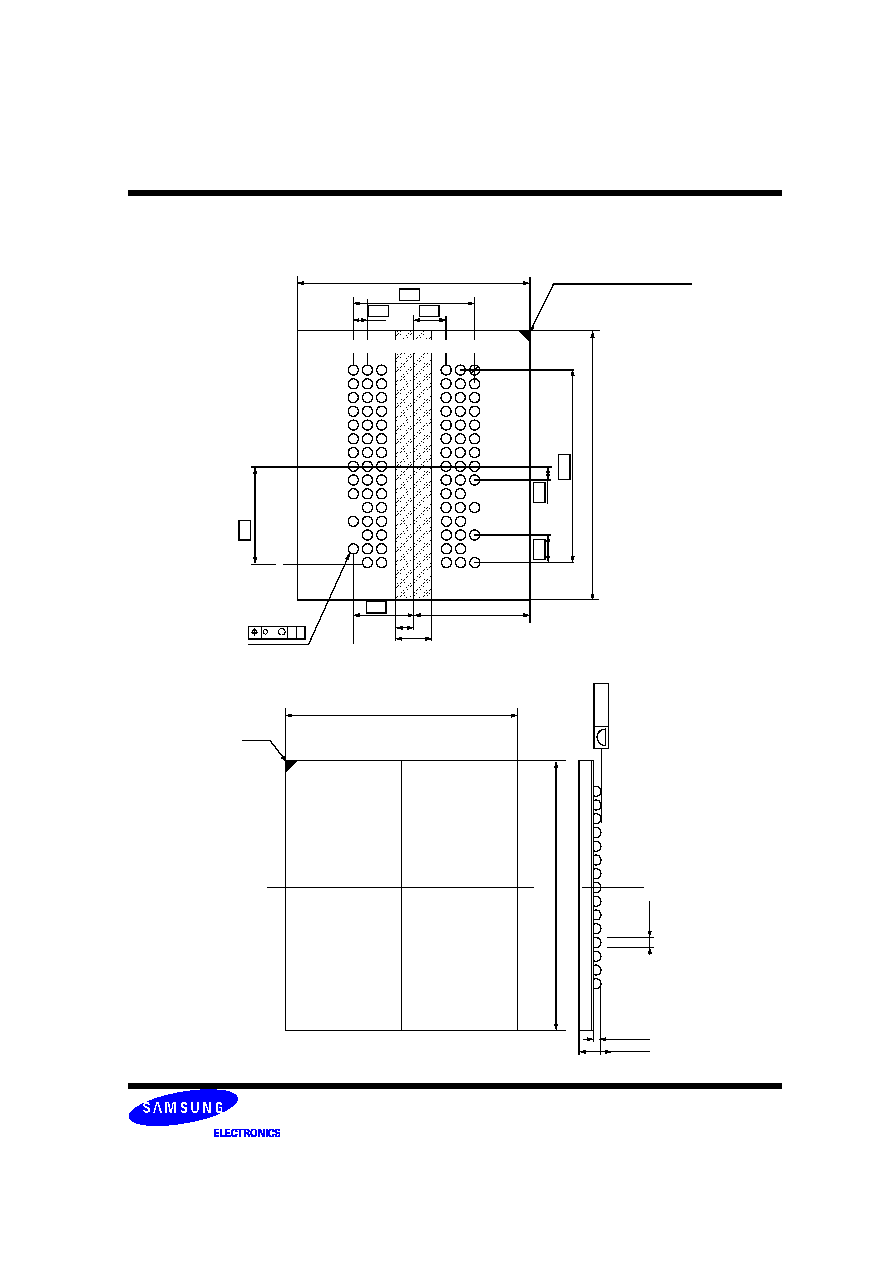
Page 11 of 38
512Mb B-die DDR2 SDRAM
Rev. 0.91 (Sep. 2003)
DDR2 SDRAM
Preliminary
FBGA Package Dimension(x16)
13.0
0
±
0.
1
0
11
.
2
0
0.
8
0
1.60
11.00
±
0.10
1
2
3
4
5
6
7
8
9
6.40
0.80
1.60
B
C
D
E
F
G
H
J
K
L
A
5.
60
(6.15)
(0.90)
(1.80)
3.20
84-
0.45
±
0.05
0.2
M A B
13.
00
±
0.
1
0
11.00
±
0.10
#A1
0.
5
0
±
0.
05
0.1
0
MAX
0.35
±
0.05
MAX.1.20
M
N
P
R
# A1 INDEX MARK (OPTIONAL)
Page 12 of 38
512Mb B-die DDR2 SDRAM
Rev. 0.91 (Sep. 2003)
DDR2 SDRAM
Preliminary
2.2 Input/Output Functional Description
Symbol
Type
Function
CK, CK
Input
Clock: CK and CK are differential clock inputs. All address and control input signals are sampled
on the crossing of the positive edge of CK and negative edge of CK. Output (read) data is refer-
enced to the crossings of CK and CK (both directions of crossing).
CKE
Input
Clock Enable: CKE HIGH activates, and CKE Low deactivates, internal clock signals and device
input buffers and output drivers. Taking CKE Low provides Precharge Power-Down and Self
Refresh operation (all banks idle), or Active Power-Down (row Active in any bank). CKE is syn-
chronous for power down entry and exit, and for self refresh entry. CKE is asynchronous for self
refresh exit. CKE must be maintained high throughout read and write accesses. Input buffers,
excluding CK, CK, ODT and CKE are disabled during power-down. Input buffers, excluding CKE,
are disabled during self refresh.
CS
Input
Chip Select: All commands are masked when CS is registered HIGH. CS provides for external
Rank selection on systems with multiple Ranks. CS is considered part of the command code.
ODT
Input
On Die Termination: ODT (registered HIGH) enables termination resistance internal to the DDR2
SDRAM. When enabled, ODT is only applied to each DQ, DQS, DQS, RDQS, RDQS, and DM
signal for x4x8 configurations. For x16 configuration ODT is applied to each DQ, UDQS/UDQS,
LDQS/LDQS, UDM, and LDM signal. The ODT pin will be ignored if the Extended Mode Register
(EMRS) is programmed to disable ODT.
RAS, CAS, WE
Input
Command Inputs: RAS, CAS and WE (along with CS) define the command being entered.
DM
Input
Input Data Mask: DM is an input mask signal for write data. Input data is masked when DM is
sampled HIGH coincident with that input data during a Write access. DM is sampled on both
edges of DQS. Although DM pins are input only, the DM loading matches the DQ and DQS load-
ing. For x8 device, the function of DM or RDQS/RDQS is enabled by EMRS command.
BA0 - BA1
Input
Bank Address Inputs: BA0 and BA1 for 256 and 512Mb, BA0 - BA2 define to which bank an
Active, Read, Write or Precharge command is being applied. Bank address also determines if the
mode register or extended mode register is to be accessed during a MRS or EMRS cycle.
A0 - A13
Input
Address Inputs: Provided the row address for Active commands and the column address and
Auto Precharge bit for Read/Write commands to select one location out of the memory array in the
respective bank. A10 is sampled during a Precharge command to determine whether the Pre-
charge applies to one bank (A10 LOW) or all banks (A10 HIGH). If only one bank is to be pre-
charged, the bank is selected by BA0, BA1. The address inputs also provide the op-code during
Mode Register Set commands.
DQ
Input/Output Data Input/ Output: Bi-directional data bus.
DQS, (DQS)
(LDQS), (LDQS)
(UDQS), (UDQS)
(RDQS), (RDQS)
Input/Output
Data Strobe: output with read data, input with write data. Edge-aligned with read data, centered in
write data. For the x16, LDQS corresponds to the data on DQ0-DQ7; UDQS corresponds to the
data on DQ8-DQ15. For the x8, an RDQS option using DM pin can be enabled via the EMRS(1) to
simplify read timing. The data strobes DQS, LDQS, UDQS, and RDQS may be used in single
ended mode or paired with optional complementary signals DQS, LDQS, UDQS, and RDQS to
provide differential pair signaling to the system during both reads and writes. An EMRS(1) control
bit enables or disables all complementary data strobe signals.
NC
No Connect: No internal electrical connection is present.
V
DDQ
Supply
DQ Power Supply: 1.8V +/- 0.1V
V
SSQ
Supply
DQ Ground
V
DDL
Supply
DLL Power Supply: 1.8V +/- 0.1V
V
SSDL
Supply
DLL Ground
V
DD
Supply
Power Supply: 1.8V +/- 0.1V
V
SS
Supply
Ground
V
REF
Supply
Reference voltage
In this data sheet, "differential DQS signals" refers to any of the following with A10 = 0 of EMRS(1)
x4 DQS/DQS
x8 DQS/DQS
if EMRS(1)[A11] = 0
x8 DQS/DQS, RDQS/RDQS,
if EMRS(1)[A11] = 1
x16 LDQS/LDQS and UDQS/UDQS
"single-ended DQS signals" refers to any of the following with A10 = 1 of EMRS(1)
x4 DQS
x8 DQS
if EMRS(1) [A11] = 0
x8 DQS, RDQS,
if EMRS(1) [A11] = 1
x16 LDQS and UDQS
Page 13 of 38
512Mb B-die DDR2 SDRAM
Rev. 0.91 (Sep. 2003)
DDR2 SDRAM
Preliminary
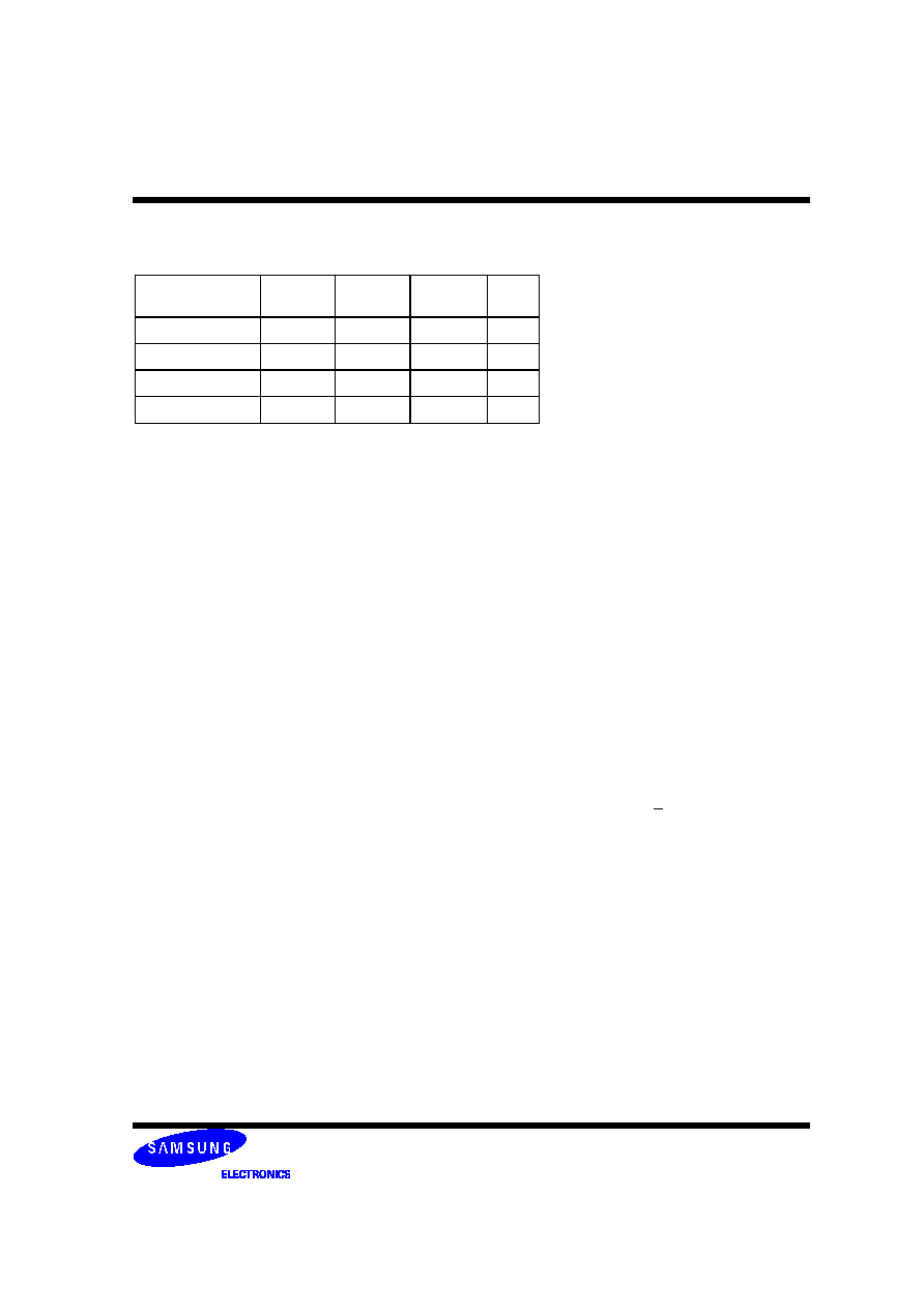
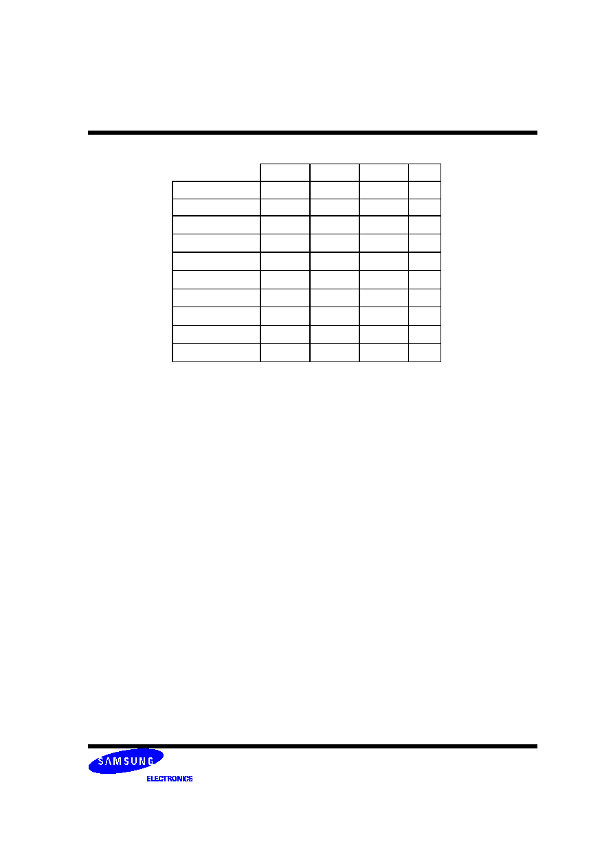
2.3 512Mb Addressing
* Reference information: The following tables are address mapping information for other densities.
256Mb
1Gb
2Gb
4Gb
Configuration
128Mb x4
64Mb x 8
32Mb x16
# of Bank
4
4
4
Bank Address
BA0,BA1
BA0,BA1
BA0,BA1
Auto precharge
A
10
/AP
A
10
/AP
A
10
/AP
Row Address
A
0
~ A
13
A
0
~ A
13
A
0
~ A
12
Column Address
A
0
~ A
9,
A
11
A
0
~ A
9
A
0
~ A
9
Configuration
64Mb x4
32Mb x 8
16Mb x16
# of Bank
4
4
4
Bank Address
BA0,BA1
BA0,BA1
BA0,BA1
Auto precharge
A
10
/AP
A
10
/AP
A
10
/AP
Row Address
A
0
~ A
12
A
0
~ A
12
A
0
~ A
12
Column Address
A
0
~ A
9,
A
11
A
0
~ A
9
A
0
~ A
8
Configuration
256Mb x4
128Mb x 8
64Mb x16
# of Bank
8
8
8
Bank Address
BA0 ~ BA2
BA0 ~ BA2
BA0 ~ BA2
Auto precharge
A
10
/AP
A
10
/AP
A
10
/AP
Row Address
A
0
~ A
13
A
0
~ A
13
A
0
~ A
12
Column Address
A
0
~ A
9,
A
11
A
0
~ A
9
A
0
~ A
9
Configuration
512Mb x4
256Mb x 8
128Mb x16
# of Bank
8
8
8
Bank Address
BA0 ~ BA2
BA0 ~ BA2
BA0 ~ BA2
Auto precharge
A
10
/AP
A
10
/AP
A
10
/AP
Row Address
A
0
~ A
14
A
0
~ A
14
A
0
~ A
13
Column Address
A
0
~ A
9,
A
11
A
0
~ A
9
A
0
~ A
9
Configuration
1 Gb x4
512Mb x 8
256Mb x16
# of Bank
8
8
8
Bank Address
BA0 ~ BA2
BA0 ~ BA2
BA0 ~ BA2
Auto precharge
A
10
/AP
A
10
/AP
A
10
/AP
Row Address
tbd
tbd
tbd
Column Address/page size
tbd
tbd
tbd
Page 14 of 38
512Mb B-die DDR2 SDRAM
Rev. 0.91 (Sep. 2003)
DDR2 SDRAM
Preliminary
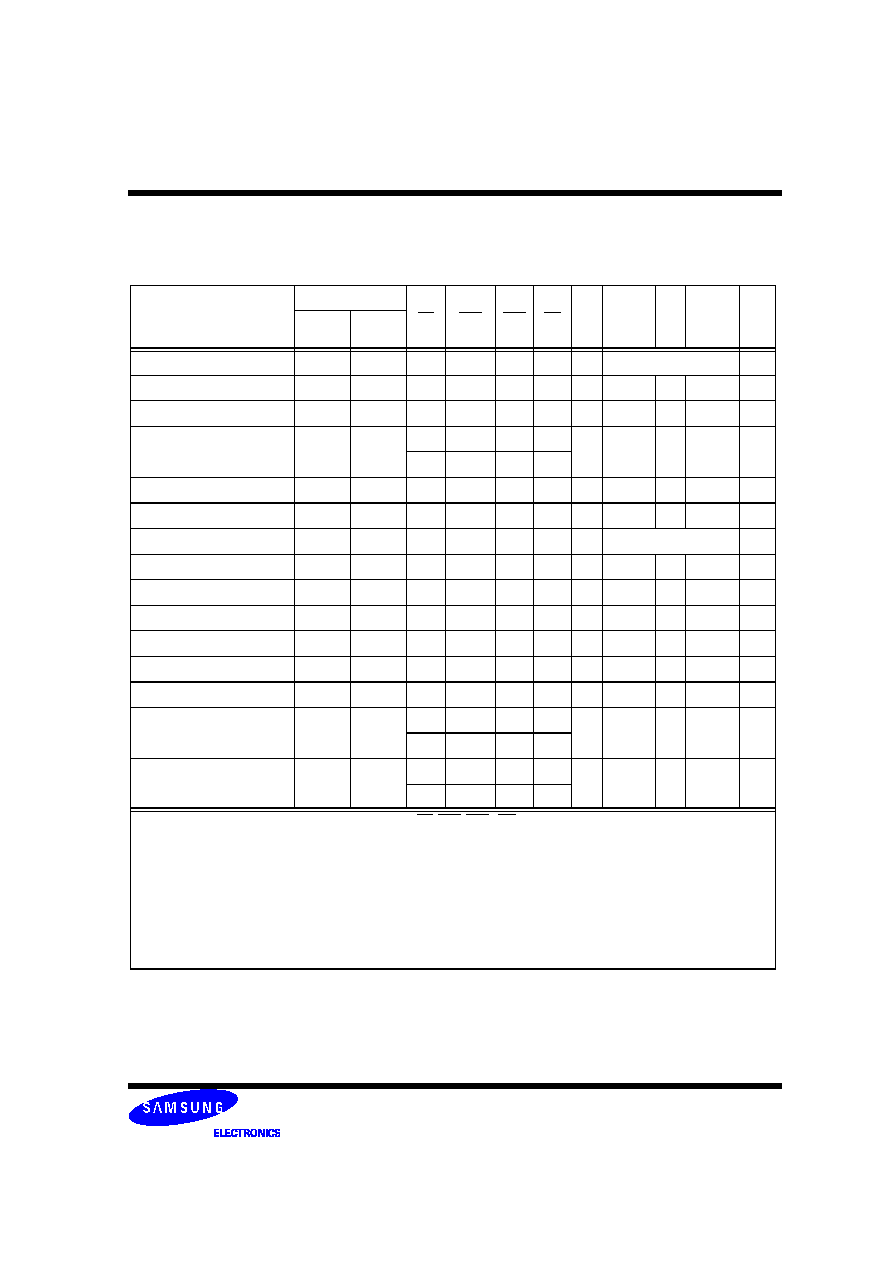
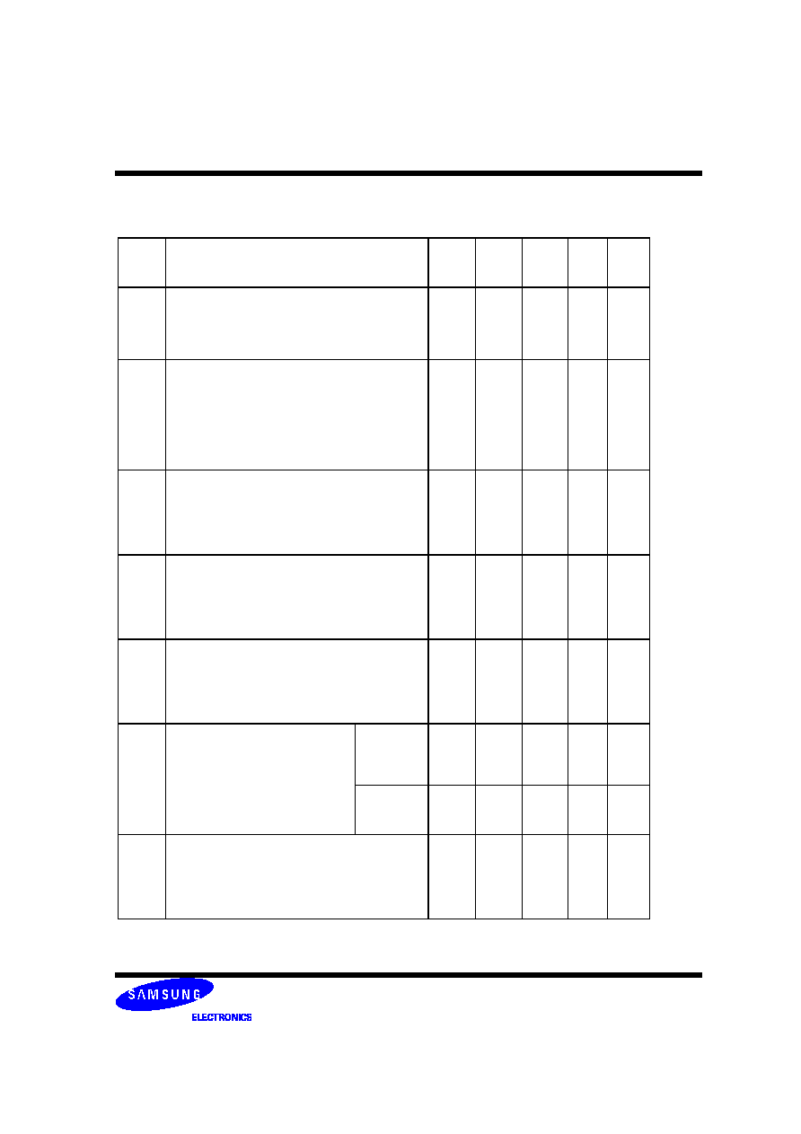
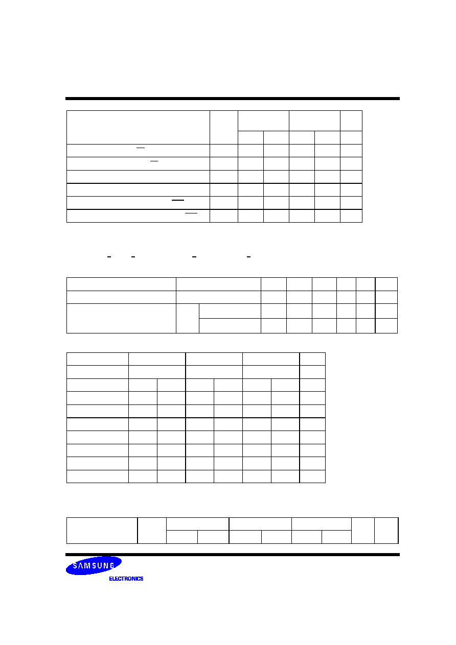
3. Command Truth Table.
3.1 Command truth table.
Function
CKE
CS
RAS CAS
WE
BA0
BA1
BA2
A15-A11 A10
A9 - A0
Notes
Previous
Cycle
Current
Cycle
(Extended) Mode Register Set
H
H
L
L
L
L
BA
OP Code
1,2
Refresh (REF)
H
H
L
L
L
H
X
X
X
X
1
Self Refresh Entry
H
L
L
L
L
H
X
X
X
X
1
Self Refresh Exit
L
H
H
X
X
X
X
X
X
X
1,7
L
H
H
H
Single Bank Precharge
H
H
L
L
H
L
BA
X
L
X
1,2
Precharge all Banks
H
H
L
L
H
L
X
X
H
X
1
Bank Activate
H
H
L
L
H
H
BA
Row Address
1,2
Write
H
H
L
H
L
L
BA
Column
L
Column
1,2,3,
Write with Auto Precharge
H
H
L
H
L
L
BA
Column
H
Column
1,2,3,
Read
H
H
L
H
L
H
BA
Column
L
Column
1,2,3
Read with Auto-Precharge
H
H
L
H
L
H
BA
Column
H
Column
1,2,3
No Operation
H
X
L
H
H
H
X
X
X
X
1
Device Deselect
H
X
H
X
X
X
X
X
X
X
1
Power Down Entry
H
L
H
X
X
X
X
X
X
X
1,4
L
H
H
H
Power Down Exit
L
H
H
X
X
X
X
X
X
X
1,4
L
H
H
H
1. All DDR2 SDRAM commands are defined by states of CS, RAS, CAS , WE and CKE at the rising edge of the clock.
2. Bank addresses BA0, BA1, BA2 (BA) determine which bank is to be operated upon. For (E)MRS BA selects an (Extended) Mode
Register.
3. Burst reads or writes at BL=4 cannot be terminated or interrupted. See sections "Reads interrupted by a Read" and "Writes inter-
rupted by a Write" in section 2.2.4 for details.
4. The Power Down Mode does not perform any refresh operations. The duration of Power Down is therefore limited by the refresh
requirements outlined in section 2.2.7.
5. The state of ODT does not affect the states described in this table. The ODT function is not available during Self Refresh. See
section 2.2.2.4.
6. "X" means "H or L (but a defined logic level)".
7. Self refresh exit is asynchronous.
Page 15 of 38
512Mb B-die DDR2 SDRAM
Rev. 0.91 (Sep. 2003)
DDR2 SDRAM
Preliminary
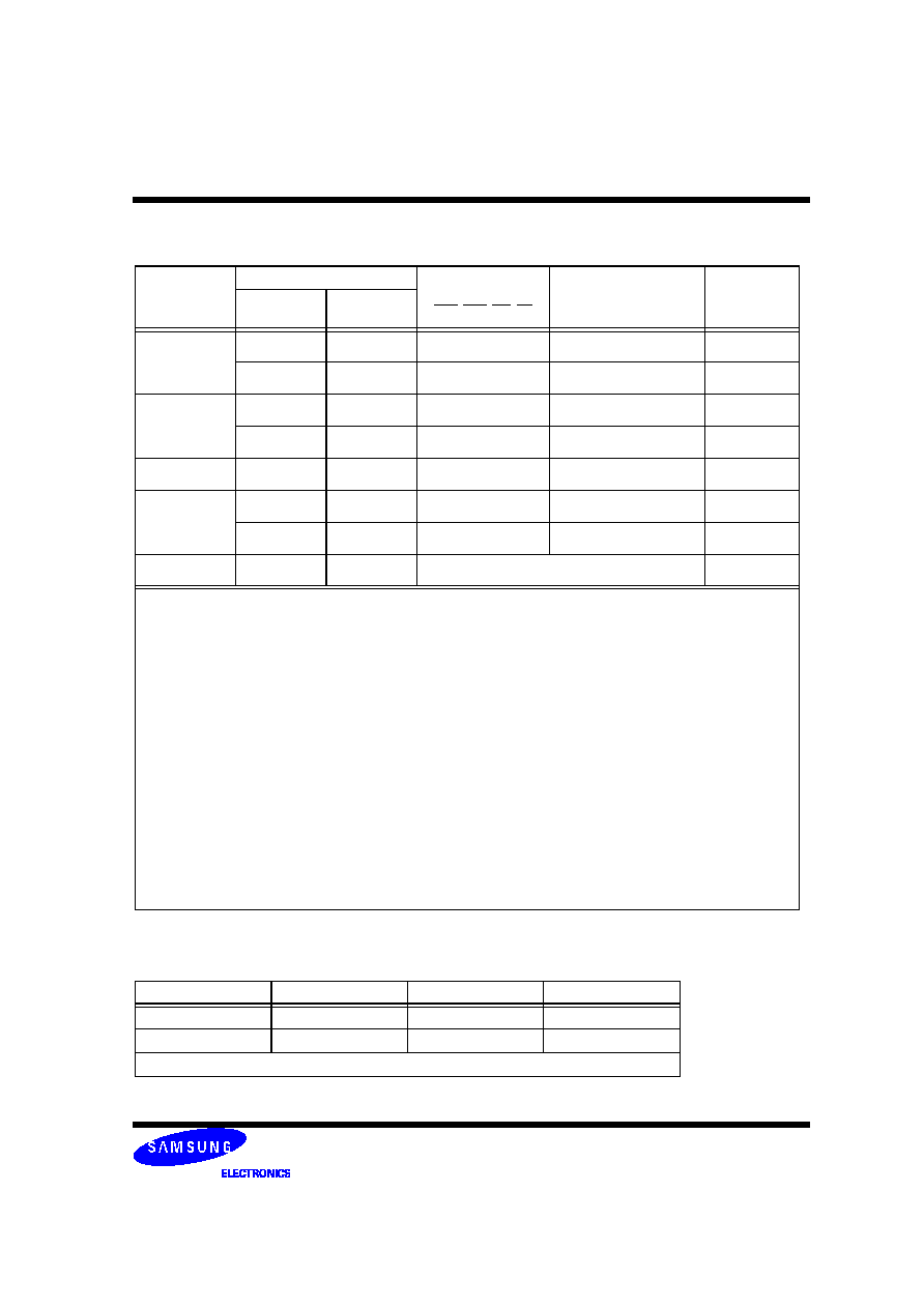
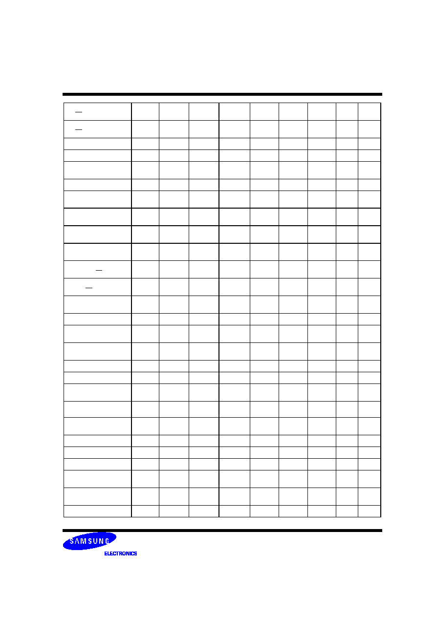
3.2 Clock Enable (CKE) Truth Table for Synchronous Transitions
Current State
2
CKE
Command (N)
3
RAS, CAS, WE, CS
Action (N)
3
Notes
Previous Cycle
1
(N-1)
Current Cycle
1
(N)
Power Down
L
L
X
Maintain Power-Down
11, 13, 15
L
H
DESELECT or NOP
Power Down Exit
4, 8, 11,13
Self Refresh
L
L
X
Maintain Self Refresh
11, 15
L
H
DESELECT or NOP
Self Refresh Exit
4, 5,9
Bank(s) Active
H
L
DESELECT or NOP
Active Power Down Entry
4,8,10,11,13
All Banks Idle
H
L
DESELECT or NOP
Precharge Power Down Entry
4, 8, 10,11,13
H
L
REFRESH
Self Refresh Entry
6, 9, 11,13
H
H
Refer to the Command Truth Table
7
Notes:
1. CKE (N) is the logic state of CKE at clock edge N; CKE (N≠1) was the state of CKE at the previous clock edge.
2. Current state is the state of the DDR SDRAM immediately prior to clock edge N.
3. COMMAND (N) is the command registered at clock edge N, and ACTION (N) is a result of COMMAND (N).
4. All states and sequences not shown are illegal or reserved unless explicitly described elsewhere in this document.
5. On Self Refresh Exit DESELECT or NOP commands must be issued on every clock edge occurring during the t
XSNR
period.
Read commands may be issued only after t
XSRD
(200 clocks) is satisfied.
6. Self Refresh mode can only be entered from the All Banks Idle state.
7. Must be a legal command as defined in the Command Truth Table.
8. Valid commands for Power Down Entry and Exit are NOP and DESELECT only.
9. Valid commands for Self Refresh Exit are NOP and DESELECT only.
10. Power Down and Self Refresh can not be entered while Read or Write operations, (Extended) Mode Register Set operations or
Precharge operations are in progress. See section 2.2.9 "Power Down" and 3.2.8 "Self Refresh Command" for a detailed list of
restrictions.
11. Minimum CKE high time is three clocks.; minimum CKE low time is three clocks.
12. The state of ODT does not affect the states described in this table. The ODT function is not available during Self Refresh. See
section 2.2.2.4.
13. The Power Down does not perform any refresh operations. The duration of Power Down Mode is therefore limited by the refresh
requirements outlined in section 2.2.7.
14. CKE must be maintained high while the SDRAM is in OCD calibration mode .
15. "X" means "don't care (including floating around VREF)" in Self Refresh and Power Down. However ODT must be driven high or
low in Power Down if the ODT function is enabled (Bit A2 or A6 set to "1" in EMRS(1) ).
3.3 DM Truth Table
Name (Functional)
DM
DQs
Note
Write enable
-
Valid
1
Write inhibit
H
X
1
1. Used to mask write data, provided coincident with the corresponding data
Page 16 of 38
512Mb B-die DDR2 SDRAM
Rev. 0.91 (Sep. 2003)
DDR2 SDRAM
Preliminary
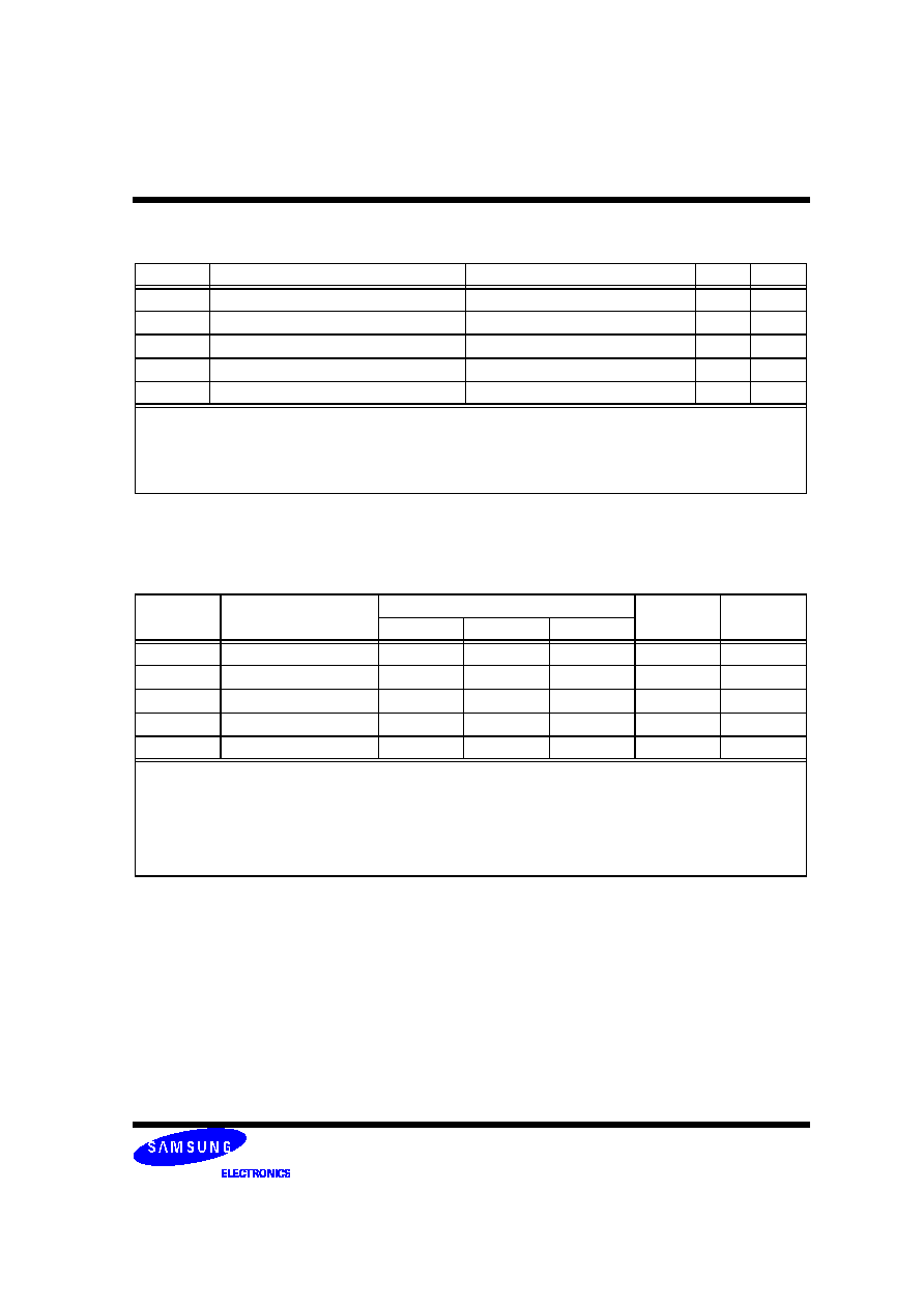
4. Absolute Maximum DC Ratings
5. AC & DC Operating Conditions
Recommended DC Operating Conditions (SSTL - 1.8)
Symbol
Parameter Rating
Units
Notes
VDD
Voltage on VDD pin relative to Vss
- 1.0 V ~ 2.3 V
V
1
VDDQ
Voltage on VDDQ pin relative to Vss
- 0.5 V ~ 2.3 V
V
1
VDDL
Voltage on VDDL pin relative to Vss
- 0.5 V ~ 2.3 V
V
1
V
IN
,
V
OUT
Voltage on any pin relative to Vss
- 0.5 V ~ 2.3 V
V
1
T
STG
Storage Temperature
-55 to +100
∞
C 1
1.
Stresses greater than those listed under "Absolute Maximum Ratings" may cause permanent damage to the device. This is a
stress rating only and functional operation of the device at these or any other conditions above those indicated in the operational
sections of this specification is not implied. Exposure to absolute maximum rating conditions for extended periods may affect reli-
ability.
2. Storage Temperature is the case surface temperature on the center/top side of the DRAM.
Symbol
Parameter
Rating
Units
Notes
Min.
Typ. Max.
VDD
Supply Voltage
1.7
1.8
1.9
V
VDDL
Supply Voltage for DLL
1.7
1.8
1.9
V
4
VDDQ
Supply Voltage for Output
1.7
1.8
1.9
V
4
VREF
Input Reference Voltage
0.49*VDDQ
0.50*VDDQ
0.51*VDDQ
mV
1.2
VTT
Termination Voltage
V
REF
-0.04
V
REF
V
REF
+0.04
V
3
There is no specific device VDD supply voltage requirement for SSTL-1.8 compliance. However under all conditions VDDQ must
be less than or equal to VDD.
1. The value of VREF may be selected by the user to provide optimum noise margin in the system. Typically the value of VREF is
expected to be about 0.5 x VDDQ of the transmitting device and VREF is expected to track variations in VDDQ.
2. Peak to peak ac noise on VREF may not exceed +/-2% VREF (dc).
3. VTT of transmitting device must track VREF of receiving device.
4. VDDQ tracks with VDD, VDDL tracks with VDD. AC parameters are measured with VDD, VDDQ and VDDDL tied together.
Page 17 of 38
512Mb B-die DDR2 SDRAM
Rev. 0.91 (Sep. 2003)
DDR2 SDRAM
Preliminary
Operating Temperature Condition
Note :
1. Operating Temperature is the case surface temperature on the center/top side of the DRAM.
2. The operation temperature range are the temperature where all DRAM specification will be supported.
Input DC Logic Level
Input AC Logic Level
AC Input Test Conditions
Note :
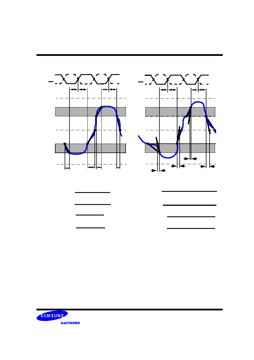
1. Setup (tIS & tDS) nominal slew rate for a rising signal is defined as the slew rate between the last crossing of Vih(dc)min and the
first crossing of Vih(ac)min. Setup (tIS & tDS) nominal slew rate for a falling signal is defined as the slew rate between the last
crossing of Vil(dc)max and the first crossing of Vil(ac)max. If the actual signal is always earlier than the nominal slew rate line
between shaded `dc to ac region', use nominal slew rate for derating value (see Fig a.) If the actual signal is later than the nominal
slew rate line anywhere between shaded `dc to ac region', the slew rate of a tangent line to the actual signal from the ac level to dc
level is used for derating value (see Fig b.)
2. Hold (tIH & tDH) nominal slew rate for a rising signal is defined as the slew rate between the last crossing of Vil(dc)max and the first
crossing of Vref. Hold (tIH & tDH) nominal slew rate for a falling signal is defined as the slew rate between the last crossing of
Vih(dc)min and the first crossing of Vref. If the actual signal is always later than the nominal slew rate line between shaded `dc to
Vref region', use nominal slew rate for derating value (see Fig a.) If the actual signal is earlier than the nominal slew rate line any-
where between shaded `dc to Vref region', the slew rate of a tangent line to the actual signal from the dc level to Vref level is used
for derating value (see Fig b.)Input waveform timing is referenced to the input signal crossing through the V
REF
level applied to the
device under test.
SYMBOL
PARAMETER
RATING
UNITS
NOTES
TOPER
Operating Temperature
0 to 95
∞
C 1,
2
Symbol
Parameter
Min.
Max.
Units
Notes
V
IH
(dc)
dc input logic high
V
REF
+ 0.125
V
DDQ
+ 0.3
V
V
IL
(dc)
dc input logic low
- 0.3
V
REF
- 0.125
V
Symbol
Parameter
Min.
Max.
Units
Notes
V
IH
(dc)
dc input logic high
V
REF
+ 0.125
V
DDQ
+ 0.3
V
V
IL
(dc)
dc input logic low
- 0.3
V
REF
- 0.125
V
Symbol
Parameter
Min.
Max.
Units
Notes
V
IH
(ac)
ac input logic high
V
REF
+ 0.250
-
V
V
IL
(ac)
ac input logic low
-
V
REF
- 0.250
V
Symbol
Condition
Value
Units
Notes
V
REF
Input reference voltage
0.5 * V
DDQ
V
1
V
SWING(MAX)
Input signal maximum peak to peak swing
1.0
V
1
SLEW
Input signal minimum slew rate
1.0
V/ns
2, 3
Page 18 of 38
512Mb B-die DDR2 SDRAM
Rev. 0.91 (Sep. 2003)
DDR2 SDRAM
Preliminary
V
SS
DQS
DQS
Hold
Setup
Hold
Setup Slew Rate
Setup Slew Rate
Rising Signal
Falling Signal
Setup
Setup
Vil(dc)max - Vil(ac)max
Setup Delta TF
Vih(ac)min - Vih(dc)min
Setup Delta TR
=
V
DDQ
V
IH(ac)
min
V
IH(dc)
min
V
REF
V
IL(dc)
max
V
IL(ac)
max
Setup
dc to ac
region
dc to ac
region
Hold
Delta TF
Delta TF
Delta TR
Hold
Delta TR
=
Hold Slew Rate
Hold Slew Rate
Falling Signal
Rising Signal
Vref - Vil(dc)max
Hold Delta TR
=
Vih(dc)min - Vref
Hold Delta TF
=
V
SS
CK
CK
Setup Slew Rate
Setup Slew Rate
Rising Signal
Falling Signal
Setup
Setup
tangent line[Vil(dc)max - Vil(ac)max]
Setup Delta TF
=
tangent line[Vih(ac)min - Vih(dc)min]
Setup Delta TR
=
V
DDQ
V
IH(ac)
min
V
IH(dc)
min
V
REF
V
IL(dc)
max
V
IL(ac)
max
dc to ac
region
dc to ac
region
Hold
Hold
Hold Slew Rate
tangent line [ Vih(dc)min - Vref ]
Hold Delta TF
=
Falling Signal
Hold Slew Rate
tangent line [ Vref - Vil(dc)max ]
Hold Delta TR
=
Rising Signal
<Figure. a>
<Figure. b>
Delta TF
Delta TR
Delta TR
Delta TF
Time
Time
Time
Time
Hold
Time
Hold
Time
Setup
Time
Setup
Time
Page 19 of 38
512Mb B-die DDR2 SDRAM
Rev. 0.91 (Sep. 2003)
DDR2 SDRAM
Preliminary
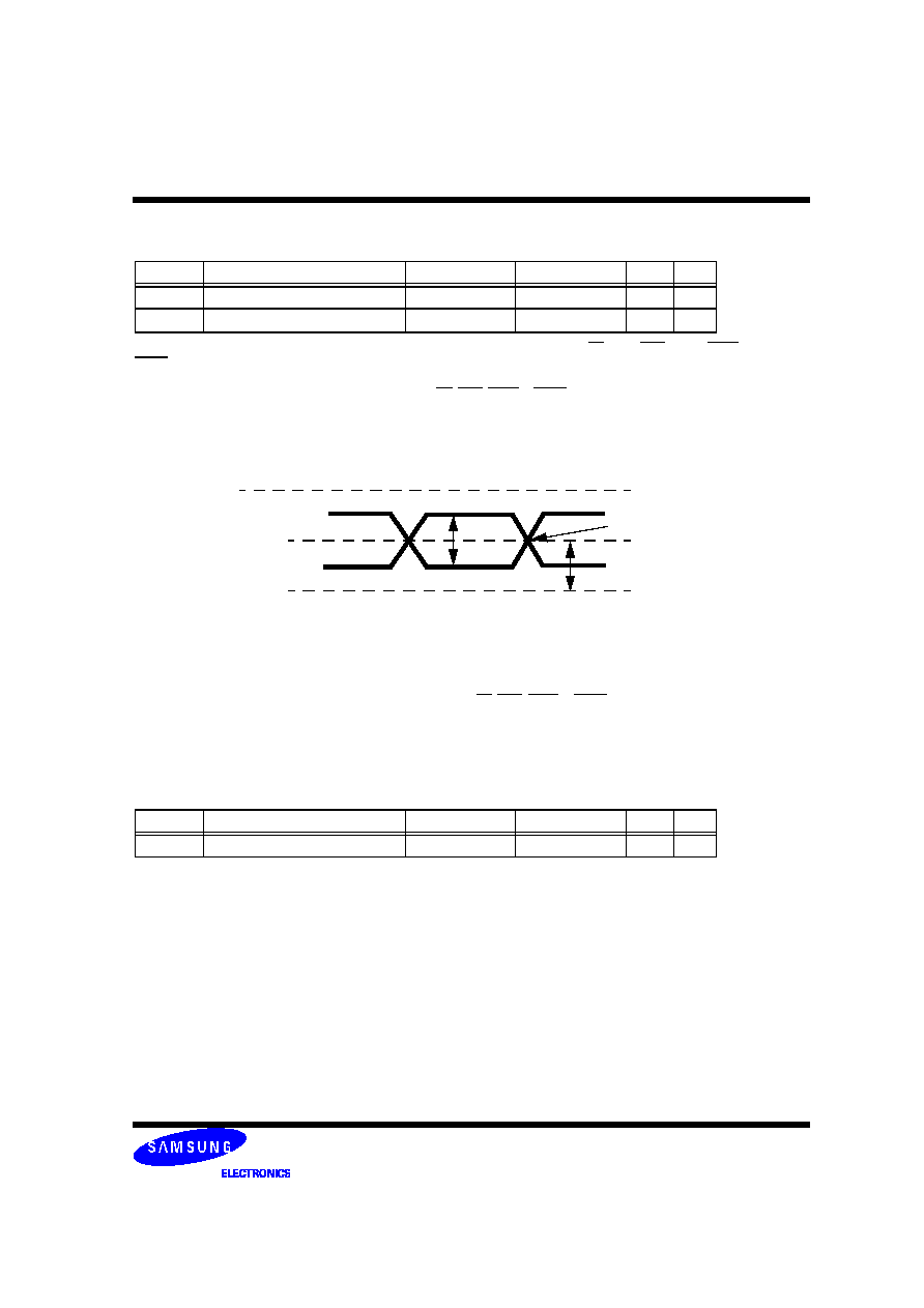
Differential input AC logic Level
1. V
IN(DC)
specifies the allowable DC execution of each input of differential pair such as CK, CK, DQS, DQS, LDQS, LDQS, UDQS and
UDQS.
2. V
ID(DC
) specifies the input differential voltage |V
TR
-V
CP
| required for switching, where V
TR
is the true input (such as CK, DQS, LDQS
or UDQS) level and V
CP
is the complementary input (such as CK, DQS, LDQS or UDQS) level. The minimum value is equal to V
IH(DC)
- V
IL(DC)
.
Notes:
1. V
ID(AC)
specifies the input differential voltage |V
TR
-V
CP
| required for switching, where V
TR
is the true input signal (such as CK, DQS,
LDQS or UDQS) and V
CP
is the complementary input signal (such as CK, DQS, LDQS or UDQS). The minimum value is equal to V
IH(AC)
- V
IL(AC)
.
2. The typical value of V
IX(AC)
is expected to be about 0.5 * VDDQ of the transmitting device and V
IX(AC)
is expected to track variations in
VDDQ . V
IX(AC)
indicates the voltage at which differential input signals must cross.
Differential AC output parameters
Notes:
1. The typical value of V
OX(AC)
is expected to be about 0.5 * V DDQ of the transmitting device and V
OX(AC
) is expected to track variations
in VDDQ . V
OX(AC)
indicates the voltage at whitch differential output signals must cross.
Symbol
Parameter
Min.
Max.
Units
Notes
V
ID
(ac)
ac differential input voltage
0.5
V
DDQ
+ 0.6
V
1
V
IX
(ac)
ac differential cross point voltage
0.5 * VDDQ - 0.175
0.5 * VDDQ + 0.175
V
2
Symbol
Parameter
Min.
Max.
Units
Notes
V
OX
(ac)
ac differential cross point voltage
0.5 * VDDQ - 0.125
0.5 * VDDQ + 0.125
V
1
V
DDQ
Crossing point
V
SSQ
V
TR
V
CP
V
ID
V
IX or
V
OX
< Differential signal levels >
Page 20 of 38
512Mb B-die DDR2 SDRAM
Rev. 0.91 (Sep. 2003)
DDR2 SDRAM
Preliminary
Input Signal Overshoot/Undershoot Specification
AC Overshoot/Undershoot Specification for Address and Control Pins A0-A15, BA0-BA2, CS, RAS,
CAS, WE, CKE, ODT
Parameter
Specification
DDR2-400
DDR2-533
DDR2-667
Maximum peak amplitude allowed for overshoot area (See Figure 1):
0.9V
0.9V
0.9V
Maximum peak amplitude allowed for undershoot area (See Figure 1):
0.9V
0.9V
0.9V
Maximum overshoot area above VDD (See Figure1).
0.75 V-ns
0.56 V-ns
0.45 V-ns
Maximum undershoot area below VSS (See Figure 1).
0.75 V-ns
0.56 V-ns
0.45 V-ns
AC Overshoot/Undershoot Specification for Clock, Data, Strobe, and Mask Pins DQ, DQS, DM, CK,
CK
Parameter
Specification
DDR2-400
DDR2-533
DDR2-667
Maximum peak amplitude allowed for overshoot area (See Figure 2):
0.9V
0.9V
0.9V
Maximum peak amplitude allowed for undershoot area (See Figure 2):
0.9V
0.9V
0.9V
Maximum overshoot area above VDDQ (See Figure 2).
0.38 V-ns
0.28 V-ns
0.23 V-ns
Maximum undershoot area below VSSQ (See Figure 2).
0.38 V-ns
0.28 V-ns
0.23 V-ns
Overshoot Area
Maximum Amplitude
V
DD
Undershoot Area
Maximum Amplitude
V
SS
Volts
(V)
AC Overshoot and Undershoot Definition for Address and Control Pins
Time (ns)
Overshoot Area
Maximum Amplitude
V
DDQ
Undershoot Area
Maximum Amplitude
V
SSQ
Volts
(V)
AC Overshoot and Undershoot Definition for Clock, Data, Strobe, and Mask Pins
Time (ns)
Page 21 of 38
512Mb B-die DDR2 SDRAM
Rev. 0.91 (Sep. 2003)
DDR2 SDRAM
Preliminary
Power and ground clamps are implemented on the following input only pins:
1. BA0-BA2
2. A0-A15
3. RAS
4. CAS
5. WE
6. CS
7. ODT
8. CKE
V-I Characteristics for input only pins with clamps
Voltage across
clamp(V)
Minimum Power
Clamp Current (mA)
Minimum Ground
Clamp Current (mA)
0.0
0
0
0.1
0
0
0.2
0
0
0.3
0
0
0.4
0
0
0.5
0
0
0.6
0
0
0.7
0
0
0.8
0.1
0.1
0.9
1.0
1.0
1.0
2.5
2.5
1.1
4.7
4.7
1.2
6.8
6.8
1.3
9.1
9.1
1.4
11.0
11.0
1.5
13.5
13.5
1.6
16.0
16.0
1.7
18.2
18.2
1.8
21.0
21.0

Page 22 of 38
512Mb B-die DDR2 SDRAM
Rev. 0.91 (Sep. 2003)
DDR2 SDRAM
Preliminary
Output Buffer Levels
Output AC Test Conditions
Output DC Current Drive
OCD default characteristics
Note 1: Absolute Specifications (0∞C
T
CASE
+tbd∞C; VDD = +1.8V ±0.1V, VDDQ = +1.8V ±0.1V)
Note 2: Impedance measurement condition for output source dc current: VDDQ = 1.7V; VOUT = 1420mV;
(VOUT-VDDQ)/Ioh must be less than 23.4 ohms for values of VOUT between VDDQ and VDDQ-280mV.
Impedance measurement condition for output sink dc current: VDDQ = 1.7V; VOUT = 280mV; VOUT/Iol
must be less than 23.4 ohms for values of VOUT between 0V and 280mV.
Note 3: Mismatch is absolute value between pull-up and pull-dn, both are measured at same temperature and
voltage.
Note 4: Slew rate measured from vil(ac) to vih(ac).
Note 5: The absolute value of the slew rate as measured from DC to DC is equal to or greater than the slew
rate as measured from AC to AC. This is guaranteed by design and characterization.
Symbol
Parameter
SSTL_18 Class II
Units
Notes
V
OH
Minimum Required Output Pull-up under AC Test Load
V
TT
+ 0.603
V
V
OL
Maximum Required Output Pull-down under AC Test Load
V
TT
- 0.603
V
V
OTR
Output Timing Measurement Reference Level
0.5 * V
DDQ
V
1
1. The VDDQ of the device under test is referenced.
Symbol
Parameter
SSTl_18 Class II
Units
Notes
I
OH(dc)
Output Minimum Source DC Current
- 13.4
mA
1, 3, 4
I
OL(dc)
Output Minimum Sink DC Current
13.4
mA
2, 3, 4
1.
V
DDQ
= 1.7 V; V
OUT
= 1420 mV. (V
OUT
- V
DDQ
)/I
OH
must be less than 21 ohm for values of V
OUT
between V
DDQ
and V
DDQ
- 280
mV.
2.
V
DDQ
= 1.7 V; V
OUT
= 280 mV. V
OUT
/I
OL
must be less than 21 ohm for values of V
OUT
between 0 V and 280 mV.
3.
The dc value of V
REF
applied to the receiving device is set to V
TT
4.
The values of I
OH(dc)
and I
OL(dc)
are based on the conditions given in Notes 1 and 2. They are used to test device drive current
capability to ensure V
IH
min plus a noise margin and V
IL
max minus a noise margin are delivered to an SSTL_18 receiver. The
actual current values are derived by shifting the desired driver operating point (see Section 3.3) along a 21 ohm load line to define
a convenient driver current for measurement.
Description
Parameter
Min
Nom
Max
Unit
Notes
Output impedance
12.6
18
23.4
ohms
1,2
Output impedance step
size for OCD calibration
0
1.5
ohms
6
Pull-up and pull-down
mismatch
0
4
ohms
1,2,3
Output slew rate
tbd
tbd
V/ns
1,4,5

Page 23 of 38
512Mb B-die DDR2 SDRAM
Rev. 0.91 (Sep. 2003)
DDR2 SDRAM
Preliminary
Note 6 : This represents the step size when the OCD is near 18 ohms at nominal conditions across all
process and represents only the DRAM uncertainty. A 0 ohm value (no calibration) can only be achieved if the
OCD impedance is 18 ohms +/- 0.75 ohms under nominal conditions.
Output slew rate load :
25 ohms
V
TT
Output
(V
OUT)
Reference
Point
Page 24 of 38
512Mb B-die DDR2 SDRAM
Rev. 0.91 (Sep. 2003)
DDR2 SDRAM
Preliminary
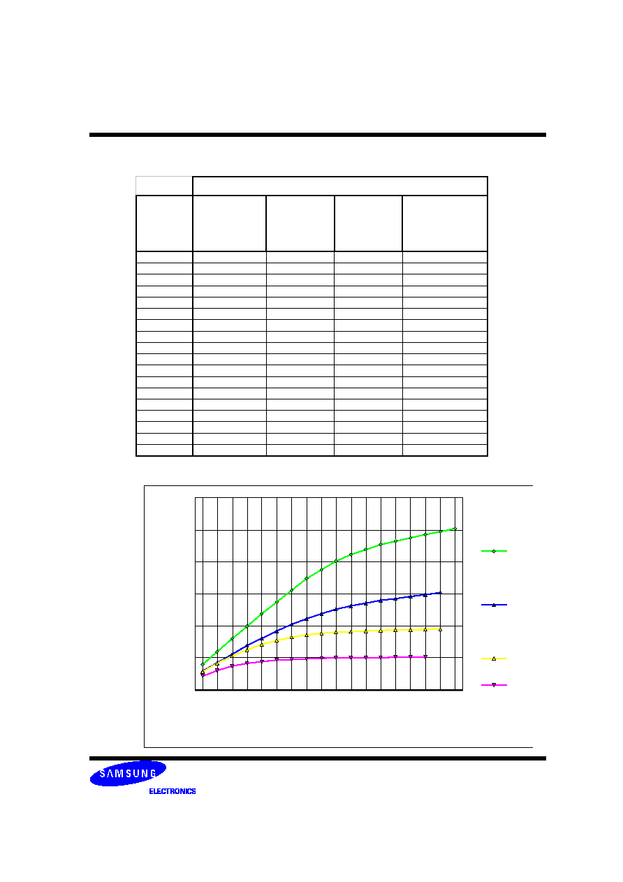
Table 1. Full Strength Default Pulldown Driver Characteristics
Figure 1. DDR2 Default Pulldown Characteristics for Full Strength Driver
Pulldow n Current (mA)
Voltage (V) Minimum (23.4 Ohms)
Nominal Default
Low (18 ohms)
Nominal Default
High (18 ohms)
Maximum (12.6 Ohms)
0.2
8.5
11.3
11.8
15.9
0.3
12.1
16.5
16.8
23.8
0.4
14.7
21.2
22.1
31.8
0.5
16.4
25.0
27.6
39.7
0.6
17.8
28.3
32.4
47.7
0.7
18.6
30.9
36.9
55.0
0.8
19.0
33.0
40.9
62.3
0.9
19.3
34.5
44.6
69.4
1.0
19.7
35.5
47.7
75.3
1.1
19.9
36.1
50.4
80.5
1.2
20.0
36.6
52.6
84.6
1.3
20.1
36.9
54.2
87.7
1.4
20.2
37.1
55.9
90.8
1.5
20.3
37.4
57.1
92.9
1.6
20.4
37.6
58.4
94.9
1.7
20.6
37.7
59.6
97.0
1.8
37.9
60.9
99.1
1.9
101.1
0.2
0.3
0.4
0.5
0.6
0.7
0.8
0.9
1.0
1.1
1.2
1.3
1.4
1.5
1.6
1.7
1.8
1.9
VOUT to VSSQ (V)
0
20
40
60
80
100
120
Pulldown current (mA)
Maximum
Nominal
Default
High
Nominal
Default
Low
Minimum
Page 25 of 38
512Mb B-die DDR2 SDRAM
Rev. 0.91 (Sep. 2003)
DDR2 SDRAM
Preliminary
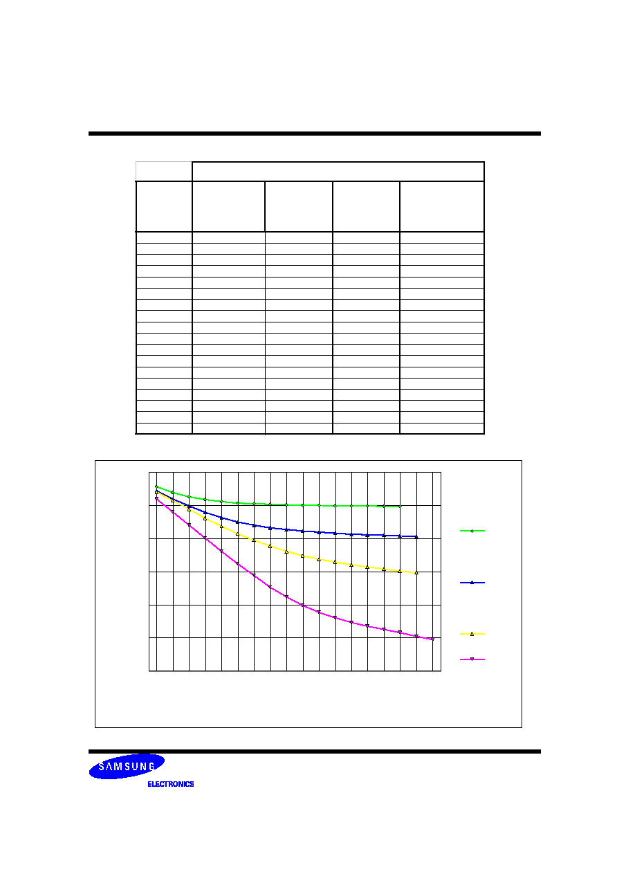
Table 2. Full Strength Default Pullup Driver Characteristics
Figure 2. DDR2 Default Pullup Characteristics for Full Strength Output Driver
Pullup Current (mA)
Voltage (V) Minimum (23.4 Ohms) Nominal Default
Low (18 ohms)
Nominal Default
High (18 ohms)
Maximum (12.6 Ohms)
0.2
-8.5
-11.1
-11.8
-15.9
0.3
-12.1
-16.0
-17.0
-23.8
0.4
-14.7
-20.3
-22.2
-31.8
0.5
-16.4
-24.0
-27.5
-39.7
0.6
-17.8
-27.2
-32.4
-47.7
0.7
-18.6
-29.8
-36.9
-55.0
0.8
-19.0
-31.9
-40.8
-62.3
0.9
-19.3
-33.4
-44.5
-69.4
1.0
-19.7
-34.6
-47.7
-75.3
1.1
-19.9
-35.5
-50.4
-80.5
1.2
-20.0
-36.2
-52.5
-84.6
1.3
-20.1
-36.8
-54.2
-87.7
1.4
-20.2
-37.2
-55.9
-90.8
1.5
-20.3
-37.7
-57.1
-92.9
1.6
-20.4
-38.0
-58.4
-94.9
1.7
-20.6
-38.4
-59.6
-97.0
1.8
-38.6
-60.8
-99.1
1.9
-101.1
0.2
0.3
0.4
0.5
0.6
0.7
0.8
0.9
1.0
1.1
1.2
1.3
1.4
1.5
1.6
1.7
1.8
1.9
VDDQ to VOUT (V)
-120
-100
-80
-60
-40
-20
0
Pullup current (mA)
Minimum
Nominal
Default
Low
Nominal
Default
High
Maximum

Page 26 of 38
512Mb B-die DDR2 SDRAM
Rev. 0.91 (Sep. 2003)
DDR2 SDRAM
Preliminary
DDR2 SDRAM Default Output Driver V≠I Characteristics
DDR2 SDRAM output driver characteristics are defined for full strength default operation as selected by
the EMRS1 bits A7-A9 = `111'. Figures 1 and 2 show the driver characteristics graphically, and tables 1 and
2 show the same data in tabular format suitable for input into simulation tools. The driver characteristics
evaluation conditions are:
Nominal Default 25
o
C (T case), VDDQ = 1.8 V, typical process
Minimum TBD
o
C (T case), VDDQ = 1.7 V, slow≠slow process
Maximum 0
o
C (T case), VDDQ = 1.9 V, fast≠fast process
Default Output Driver Characteristic Curves Notes:
1) The full variation in driver current from minimum to maximum process, temperature, and voltage will
lie within the outer bounding lines of the V≠I curve of figures 1 and 2.
2) It is recommended that the "typical" IBIS V≠I curve lie within the inner bounding lines of the V≠I curves
of figures 1 and 2.
Table 3. Full Strength Calibrated Pulldown Driver Characteristics
Table 4. Full Strength Calibrated Pullup Driver Characteristics
DDR2 SDRAM Calibrated Output Driver V≠I Characteristics
DDR2 SDRAM output driver characteristics are defined for full strength calibrated operation as selected by
the procedure outlined in section 2.2.2.3, Off-Chip Driver (OCD) Impedance Adjustment. Tables 3 and 4
show the data in tabular format suitable for input into simulation tools. The nominal points represent a
device at exactly 18 ohms. The nominal low and nominal high values represent the range that can be
achieved with a maximum 1.5 ohm step size with no calibration error at the exact nominal conditions only
(i.e. perfect calibration procedure, 1.5 ohm maximum step size guaranteed by specification). Real system
calibration error needs to be added to these values. It must be understood that these V-I curves as repre-
sented here or in supplier IBIS models need to be adjusted to a wider range as a result of any system cali-
bration error. Since this is a system specific phenomena, it cannot be quantified here. The values in the
calibrated tables represent just the DRAM portion of uncertainty while looking at one DQ only. If the cali
Calibrated Pulldow n Current (mA)
Voltage (V)
Nominal Minimum
(21 ohms)
Nominal Low (18.75
ohms)
Nominal (18 ohms)
Nominal High (17.25
ohms)
Nominal Maximum (15
ohms)
0.2
9.5
10.7
11.5
11.8
13.3
0.3
14.3
16.0
16.6
17.4
20.0
0.4
18.7
21.0
21.6
23.0
27.0
Calibrated Pullup Current (mA)
Voltage (V)
Nominal Minimum
(21 ohms)
Nominal Low (18.75
ohms)
Nominal (18 ohms)
Nominal High (17.25
ohms)
Nominal Maximum (15
ohms)
0.2
-9.5
-10.7
-11.4
-11.8
-13.3
0.3
-14.3
-16.0
-16.5
-17.4
-20.0
0.4
-18.7
-21.0
-21.2
-23.0
-27.0

Page 27 of 38
512Mb B-die DDR2 SDRAM
Rev. 0.91 (Sep. 2003)
DDR2 SDRAM
Preliminary
bration procedure is used, it is possible to cause the device to operate outside the bounds of the default
device characteristics tables and figures. In such a situation, the timing parameters in the specification can-
not be guaranteed. It is solely up to the system application to ensure that the device is calibrated between the
minimum and maximum default values at all times. If this can't be guaranteed by the system calibration pro-
cedure, re-calibration policy, and uncertainty with DQ to DQ variation, then it is recommended that only the
default values be used. The nominal maximum and minimum values represent the change in impedance
from nominal low and high as a result of voltage and temperature change from the nominal condition to the
maximum and minimum conditions. If calibrated at an extreme condition, the amount of variation could be as
much as from the nominal minimum to the nominal maximum or vice versa. The driver characteristics evalu-
ation conditions are:
Nominal 25
o
C (T case), VDDQ = 1.8 V, typical process
Nominal Low and Nominal High 25
o
C (T case), VDDQ = 1.8 V, any process
Nominal Minimum TBD
o
C (T case), VDDQ = 1.7 V, any process
Nominal Maximum 0
o
C (T case), VDDQ = 1.9 V, any process
Page 28 of 38
512Mb B-die DDR2 SDRAM
Rev. 0.91 (Sep. 2003)
DDR2 SDRAM
Preliminary
IDD Specification Parameters and Test Conditions
(IDD values are for full operating range of Voltage and Temperature, Notes 1 - 5)
Sym-
bol
Proposed Conditions
DDR2-
667
(CL=5)
DDR2-
533
(CL=4)
DDR2-
400
(CL=3)
Units
Notes
IDD0
Operating one bank active-precharge current;
tCK = tCK(IDD), tRC = tRC(IDD), tRAS = tRASmin(IDD);
CKE is HIGH, CS\ is HIGH between valid commands;
Address bus inputs are SWITCHING;
Data bus inputs are SWITCHING
TBD
TBD
TBD
mA
IDD1
Operating one bank active-read-precharge current;
IOUT = 0mA;
BL = 4, CL = CL(IDD), AL = 0;
tCK = tCK(IDD), tRC = tRC (IDD), tRAS = tRASmin(IDD),
tRCD = tRCD(IDD);
CKE is HIGH, CS\ is HIGH between valid commands;
Address bus inputs are SWITCHING;
Data pattern is same as IDD4W
TBD
TBD
TBD
mA
IDD2P
Precharge power-down current;
All banks idle;
tCK = tCK(IDD);
CKE is LOW;
Other control and address bus inputs are STABLE;
Data bus inputs are FLOATING
TBD
TBD
TBD
mA
IDD2Q
Precharge quiet standby current;
All banks idle;
tCK = tCK(IDD);
CKE is HIGH, CS\ is HIGH;
Other control and address bus inputs are STABLE;
Data bus inputs are FLOATING
TBD
TBD
TBD
mA
IDD2N
Precharge standby current;
All banks idle;
tCK = tCK(IDD);
CKE is HIGH, CS\ is HIGH;
Other control and address bus inputs are SWITCHING;
Data bus inputs are SWITCHING
TBD
TBD
TBD
mA
IDD3P
Active power-down current;
All banks open;
tCK = tCK(IDD);
CKE is LOW;
Other control and address bus inputs are
STABLE;
Data bus inputs are FLOATING
Fast PDN
Exit MRS(12)
= 0mA
TBD
TBD
TBD
mA
Slow PDN
Exit MRS(12)
= 1mA
TBD
TBD
TBD
mA
IDD3N
Active standby current;
All banks open;
tCK = tCK(IDD), tRAS = tRASmax(IDD), tRP = tRP(IDD);
CKE is HIGH, CS\ is HIGH between valid commands;
Other control and address bus inputs are SWITCHING;
Data bus inputs are SWITCHING
TBD
TBD
TBD
mA
Page 29 of 38
512Mb B-die DDR2 SDRAM
Rev. 0.91 (Sep. 2003)
DDR2 SDRAM
Preliminary
Note:
1. IDD specifications are tested after the device is properly initialized
2. Input slew rate is specified by AC Parametric Test Condition
3. IDD parameters are specified with ODT disabled.
4. Data bus consists of DQ, DM, DQS, DQS\, RDQS, RDQS\, LDQS, LDQS\, UDQS, and UDQS\. IDD values must be met with all combi-
nations of EMRS bits 10 and 11.
5. Definitions for IDD
LOW is defined as Vin
VILAC(max)
HIGH is defined as Vin
VIHAC(min)
STABLE is defined as inputs stable at a HIGH or LOW level
FLOATING is defined as inputs at VREF = VDDQ/2
SWITCHING is defined as:
inputs changing between HIGH and LOW every other clock cycle (once per two clocks) for address and control
signals, and
inputs changing between HIGH and LOW every other data transfer (once per clock) for DQ signals not including
masks or strobes.
IDD4W
Operating burst write current;
All banks open, Continuous burst writes;
BL = 4, CL = CL(IDD), AL = 0;
tCK = tCK(IDD), tRAS = tRASmax(IDD), tRP = tRP(IDD);
CKE is HIGH, CS\ is HIGH between valid commands;
Address bus inputs are SWITCHING;
Data bus inputs are SWITCHING
TBD
TBD
TBD
mA
IDD4R
Operating burst read current;
All banks open, Continuous burst reads, IOUT = 0mA;
BL = 4, CL = CL(IDD), AL = 0;
tCK = tCK(IDD), tRAS = tRASmax(IDD), tRP = tRP(IDD);
CKE is HIGH, CS\ is HIGH between valid commands;
Address bus inputs are SWITCHING;
Data pattern is same as IDD4W
TBD
TBD
TBD
mA
IDD5B
Burst auto refresh current;
tCK = tCK(IDD);
Refresh command at every tRFC(IDD) interval;
CKE is HIGH, CS\ is HIGH between valid commands;
Other control and address bus inputs are SWITCHING;
Data bus inputs are SWITCHING
TBD
TBD
TBD
mA
IDD6
Self refresh current;
CK and CK\ at 0V;
CKE
0.2V;
Other control and address bus inputs are
FLOATING;
Data bus inputs are FLOATING
Normal
TBD
TBD
TBD
mA
Low Power
TBD
TBD
TBD
mA
IDD7
Operating bank interleave read current;
All bank interleaving reads, IOUT = 0mA;
BL = 4, CL = CL(IDD), AL = tRCD(IDD)-1*tCK(IDD);
tCK = tCK(IDD), tRC = tRC(IDD), tRRD = tRRD(IDD),
tRCD = 1*tCK(IDD);
CKE is HIGH, CS\ is HIGH between valid commands;
Address bus inputs are STABLE during DESELECTs;
Data pattern is same as IDD4R;
- Refer to the following page for detailed timing conditions
TBD
TBD
TBD
mA
Page 30 of 38
512Mb B-die DDR2 SDRAM
Rev. 0.91 (Sep. 2003)
DDR2 SDRAM
Preliminary
For purposes of IDD testing, the following parameters are to be utilized
Detailed IDD7
The detailed timings are shown below for IDD7. Changes will be required if timing parameter changes are made to the specification.
Legend: A = Active; RA = Read with Autoprecharge; D = Deselect
IDD7: Operating Current: All Bank Interleave Read operation
All banks are being interleaved at minimum tRC(IDD) without violating tRRD(IDD) using a burst length of 4. Control and address bus
inputs are STABLE during DESELECTs. IOUT = 0mA
Timing Patterns for 4 bank devices x4/ x8/ x16
-DDR2-400 3/3/3
A0 RA0 A1 RA1 A2 RA2 A3 RA3 D D D D D
-DDR2-533 4/4/4
A0 RA0 D A1 RA1 D A2 RA2 D A3 RA3 D D D D D
-DDR2-667 5/5/5
A0 RA0 D D A1 RA1 D D A2 RA2 D D A3 RA3 D D D D D
DDR2-667
DDR2-533
DDR2-400
Parameter
5-5-5
4-4-4
3-3-3
Units
CL(IDD)
5
4
3
tCK
tRCD(IDD)
15
15
15
ns
tRC(IDD)
55
55
55
ns
tRRD(IDD)-x4/x8
7.5
7.5
7.5
ns
tRRD(IDD)-x16
10
10
10
ns
tCK(IDD)
3
3.75
5
ns
tRASmin(IDD)
40
40
40
ns
tRP(IDD)
15
15
15
ns
tRFC(IDD)-512Mb
105
105
105
ns
Page 31 of 38
512Mb B-die DDR2 SDRAM
Rev. 0.91 (Sep. 2003)
DDR2 SDRAM
Preliminary
Input/Output capacitance
Electrical Characteristics & AC Timing for DDR2-667/533/400
(0
∞
C < T
CASE
< 95
∞
C; V
DDQ
= 1.8V + 0.1V; V
DD
= 1.8V + 0.1V)
Refresh Parameters by Device Density
Speed Bins and CL, tRCD, tRP, tRC and tRAS for Corresponding Bin
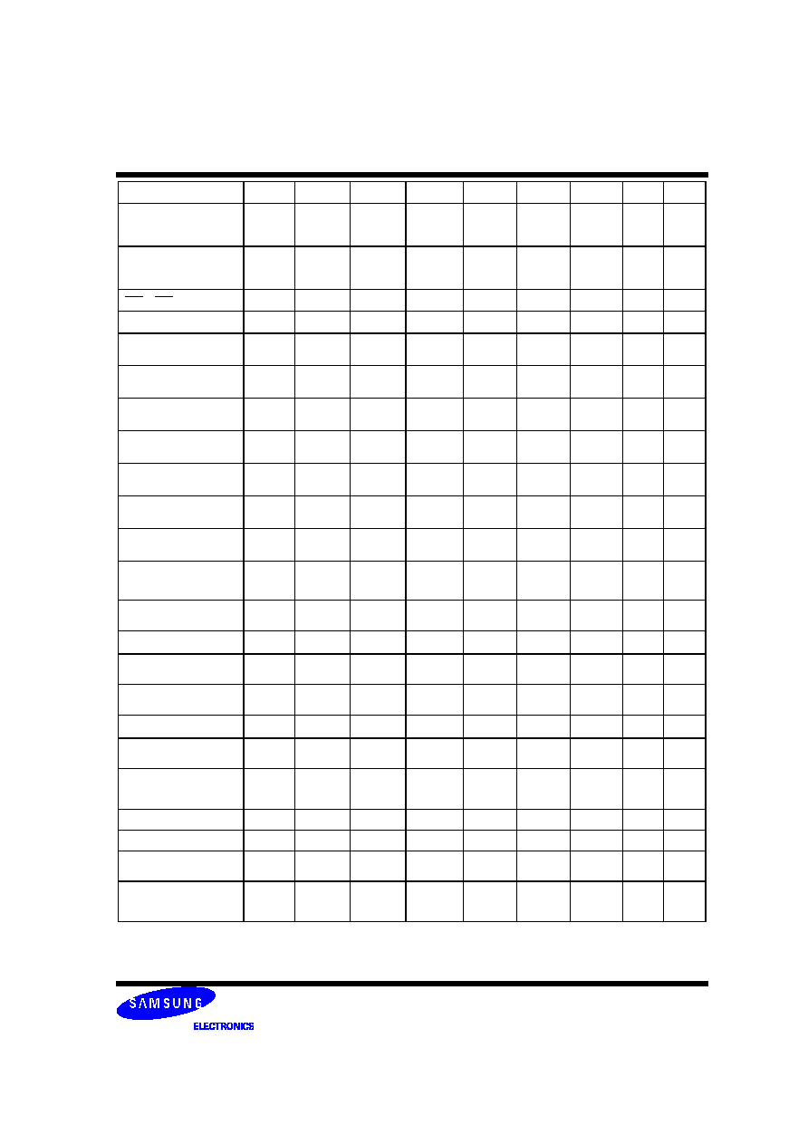
Timing Parameters by Speed Grade
(Refer to notes for informations related to this table at the bottom)
Parameter
Symbol
DDR2-400
DDR2-533
DDR2-667
Min
Max
Min
Max
Units
Input capacitance, CK and CK
CCK
1.0
2.0
1.0
2.0
pF
Input capacitance delta, CK and CK
CDCK
x
0.25
x
0.25
pF
Input capacitance, all other input-only pins
CI
1.0
2.0
1.0
2.0
pF
Input capacitance delta, all other input-only pins
CDI
x
0.25
x
0.25
pF
Input/output capacitance, DQ, DM, DQS, DQS
CIO
2.5
4.0
2.5
3.5
pF
Input/output capacitance delta, DQ, DM, DQS, DQS
CDIO
x
0.5
x
0.5
pF
Parameter
Symbol
256Mb
512Mb
1Gb
2Gb
4Gb
Units
Refresh to active/Refresh command time
tRFC
75
105
127.5
195
tbd
ns
Average periodic refresh interval
tREFI
0
∞
C
T
CASE
85
∞
C
7.8
7.8
7.8
7.8
7.8
µ
s
85
∞
C
<
T
CASE
95
∞
C
3.9
3.9
3.9
3.9
3.9
µ
s
Speed
DDR2-667(E6)
DDR2-533(D5)
DDR2-400(CC)
Units
Bin (CL - tRCD - tRP)
5 - 5- 5
4 - 4 - 4
3 - 3 - 3
Parameter
min
max
min
max
min
max
tCK, CL=3
5
8
5
8
5
8
ns
tCK, CL=4
3.75
8
3.75
8
5
8
ns
tCK, CL=5
3
8
-
-
-
-
ns
tRCD
15
15
15
ns
tRP
15
15
15
ns
tRC
55
55
55
ns
tRAS
40
70000
40
70000
40
70000
ns
Parameter
Symbol
DDR2-667
DDR2-533
DDR2-400
Units
Notes
min
max
min
max
min
max
Page 32 of 38
512Mb B-die DDR2 SDRAM
Rev. 0.91 (Sep. 2003)
DDR2 SDRAM
Preliminary
DQ output access time from
CK/CK
tAC
-450
+450
-500
+500
-600
+600
ps
DQS output access time from
CK/CK
tDQSCK
-400
+400
-450
+450
-500
+500
ps
CK high-level width
tCH
0.45
0.55
0.45
0.55
0.45
0.55
tCK
CK low-level width
tCL
0.45
0.55
0.45
0.55
0.45
0.55
tCK
CK half period
tHP
min(tCL,
tCH)
x
min(tCL,
tCH)
x
min(tCL,
tCH)
x
ps
19,20
Clock cycle time, CL=x
tCK
3000
8000
3750
8000
5000
8000
ps
23
DQ and DM input hold time
tDH
tbd
x
225
x
275
x
ps
14,15,
16
DQ and DM input setup time
tDS
tbd
x
100
x
150
x
ps
14,15,
16
Control & Address input
pulse width for each input
tIPW
0.6
x
0.6
x
0.6
x
tCK
DQ and DM input pulse width
for each input
tDIPW
0.35
x
0.35
x
0.35
x
tCK
Data-out high-impedance
time from CK/CK
tHZ
x
tAC max
x
tAC max
x
tAC max
ps
Data-out low-impedance time
from CK/CK
tLZ
tAC min
tAC max
tAC min
tAC max
tAC min
tAC max
ps
DQS-DQ skew for DQS and
associated DQ signals
tDQSQ
x
tbd
x
300
x
350
ps
21
DQ hold skew factor
tQHS
x
tbd
x
400
x
450
ps
20
DQ/DQS output hold time
from DQS
tQH
tHP -
tQHS
x
tHP - tQHS
x
tHP -
tQHS
x
ps
Write command to first DQS
latching transition
tDQSS
WL - 0.25
WL +
0.25
WL - 0.25
WL +
0.25
WL - 0.25
WL +
0.25
tCK
DQS input high pulse width
tDQSH
0.35
x
0.35
x
0.35
x
tCK
DQS input low pulse width
tDQSL
0.35
x
0.35
x
0.35
x
tCK
DQS falling edge to CK setup
time
tDSS
0.2
x
0.2
x
0.2
x
tCK
DQS falling edge hold time from
CK
tDSH
0.2
x
0.2
x
0.2
x
tCK
Mode register set command
cycle time
tMRD
2
x
2
x
2
x
tCK
Write preamble setup time
tWPRES
0
x
0
x
0
x
ps
Write postamble
tWPST
0.4
0.6
0.4
0.6
0.4
0.6
tCK
18
Write preamble
tWPRE
tbd
x
0.4
x
0.4
x
tCK
Address and control input
hold time
tIH
tbd
x
375
x
475
x
ps
13,15,
17
Address and control input
setup time
tIS
tbd
x
250
x
350
x
ps
13,15,
17
Read preamble
tRPRE
0.9
1.1
0.9
1.1
0.9
1.1
tCK
Page 33 of 38
512Mb B-die DDR2 SDRAM
Rev. 0.91 (Sep. 2003)
DDR2 SDRAM
Preliminary
General notes, which may apply for all AC parameters
1. Slew Rate Measurement Levels
Read postamble
tRPST
0.4
0.6
0.4
0.6
0.4
0.6
tCK
Active to active command
period for 1KB page size
products
tRRD
7.5
x
7.5
x
7.5
x
ns
12
Active to active command
period for
2KB page size
products
tRRD
10
x
10
x
10
x
ns
12
CAS to CAS command delay
tCCD
2
2
2
tCK
Write recovery time
tWR
15
x
15
x
15
x
ns
Auto precharge write
recovery + precharge time
tDAL
tWR+tRP*
x
tWR+tRP*
x
tWR+tRP
*
x
tCK
22
Internal write to read
command delay
tWTR
7.5
x
7.5
x
10
x
ns
Internal read to precharge
command delay
tRTP
7.5
7.5
7.5
ns
11
Exit self refresh to a non-
read command
tXSNR
tRFC + 10
tRFC + 10
tRFC +
10
ns
Exit self refresh to a read
command
tXSRD
200
200
200
tCK
Exit precharge power down
to any non-read command
tXP
2
x
2
x
2
x
tCK
Exit active power down to
read command
tXARD
2
x
2
x
2
x
tCK
9
Exit active power down to read
command
(Slow exit, Lower power)
tXARDS
6 - AL
6 - AL
6 - AL
tCK
9, 10
CKE minimum pulse width
(high and low pulse width)
t
CKE
3
3
3
tCK
ODT turn-on delay
t
AOND
2
2
2
2
2
2
tCK
ODT turn-on
t
AON
tAC(min)
tAC(max)
+0.7
tAC(min)
tAC(max)
+1
tAC(min)
tAC(max)
+1
ns
13, 24
ODT turn-on(Power-Down
mode)
t
AONPD
tAC(min)+
2
2tCK+tAC
(max)+1
tAC(min)+
2
2tCK+tAC
(max)+1
tAC(min)
+2
2tCK+tA
C(max)+1
ns
ODT turn-off delay
t
AOFD
2.5
2.5
2.5
2.5
2.5
2.5
tCK
ODT turn-off
t
AOF
tAC(min)
tAC(max)
+ 0.6
tAC(min)
tAC(max)+
0.6
tAC(min)
tAC(max)+
0.6
ns
25
ODT turn-off (Power-Down
mode)
t
AOFPD
tAC(min)+
2
2.5tCK+tA
C(max)+1
tAC(min)+
2
2.5tCK+
tAC(max)
+1
tAC(min)
+2
2.5tCK+
tAC(max)
+1
ns
ODT to power down entry latency
tANPD
3
3
3
tCK
ODT power down exit latency
tAXPD
8
8
8
tCK
OCD drive mode output
delay
tOIT
0
12
0
12
0
12
ns
Minimum time clocks
remains ON after CKE
asynchronously drops LOW
tDelay
tIS+tCK+tI
H
tIS+tCK+tI
H
tIS+tCK+t
IH
ns
23
Page 34 of 38
512Mb B-die DDR2 SDRAM
Rev. 0.91 (Sep. 2003)
DDR2 SDRAM
Preliminary
a. Output slew rate for falling and rising edges is measured between VTT - 250 mV and VTT + 250 mV for
single ended signals. For differential signals (e.g. DQS - DQS) output slew rate is measured between
DQS - DQS = -500 mV and DQS - DQS = +500mV. Output slew rate is guaranteed by design, but is not
necessarily tested on each device.
b. Input slew rate for single ended signals is measured from dc-level to ac-level: from VREF - 125 mV to
VREF + 250 mV for rising edges and from VREF + 125 mV and VREF - 250 mV for falling edges.
For differential signals (e.g. CK - CK) slew rate for rising edges is measured from CK - CK = -250 mV to
CK - CK = +500 mV
(250mV to -500 mV for falling egdes).
c. VID is the magnitude of the difference between the input voltage on CK and the input voltage on CK, or
between DQS and DQS for differential strobe.
2. DDR2 SDRAM AC timing reference load
Figure AA represents the timing reference load used in defining the relevant timing parameters of the part.
It is not intended to be either a precise representation of the typical system environment nor a depiction of the
actual load presented by a production tester. System designers will use IBIS or other simulation tools to cor-
relate the timing reference load to a system environment. Manufacturers will correlate to their production test
conditions (generally a coaxial transmission line terminated at the tester electronics).
The output timing reference voltage level for single ended signals is the crosspoint with VTT. The output tim-
ing reference voltage level for differential signals is the crosspoint of the true (e.g. DQS) and the complement
(e.g. DQS) signal.
3. DDR2 SDRAM output slew rate test load
Output slew rate is characterized under the test conditions as shown in Figure.
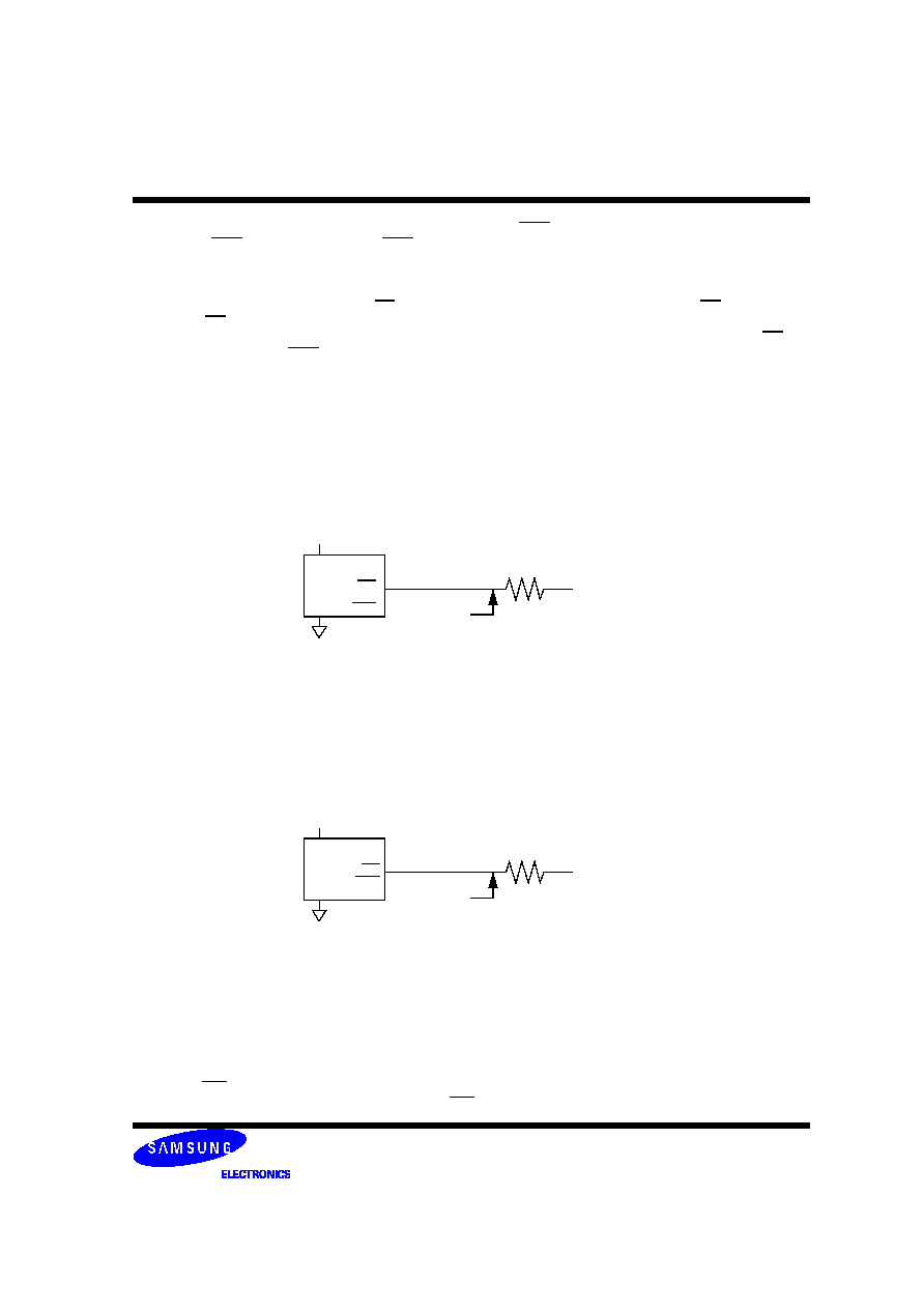
4. Differential data strobe
DDR2 SDRAM pin timings are specified for either single ended mode or differential mode depending on the setting of the EMRS
"Enable DQS" mode bit; timing advantages of differential mode are realized in system design. The method by which the DDR2 SDRAM
pin timings are measured is mode dependent. In single ended mode, timing relationships are measured relative to the rising or falling
edges of DQS crossing at VREF. In differential mode, these timing relationships are measured relative to the crosspoint of DQS and its
complement, DQS. This distinction in timing methods is guaranteed by design and characterization. Note that when differential data
strobe mode is disabled via the EMRS, the complementary pin, DQS, must be tied externally to VSS through a 20
ohm
to 10 K ohm
VDDQ
DUT
DQ
DQS
DQS
RDQS
RDQS
Output
V
TT
= V
DDQ
/2
25
Timing
reference
point
Figure AA : AC Timing Reference Load
VDDQ
DUT
DQ
DQS, DQS
RDQS, RDQS
Output
V
TT
= V
DDQ
/2
25
Test point
Slew Rate Test Load
Page 35 of 38
512Mb B-die DDR2 SDRAM
Rev. 0.91 (Sep. 2003)
DDR2 SDRAM
Preliminary
resisor to insure proper operation.
5. AC timings are for linear signal transitions. See System Derating for other signal transitions.
6. These parameters guarantee device behavior, but they are not necessarily tested on each device. They
may be guaranteed by device design or tester correlation.
7. All voltages referenced to VSS.
8. Tests for AC timing, IDD, and electrical (AC and DC) characteristics, may be conducted at nominal refer-
ence/supply voltage levels, but the related specifications and device operation are guaranteed for the full volt-
age range specified.
Specific Notes for dedicated AC parameters
9. User can choose which active power down exit timing to use via MRS(bit 12). tXARD is expected to be
used for fast active power down exit timing. tXARDS is expected to be used for slow active power down exit
timing where a lower power value is defined by each vendor data sheet.
10. AL = Additive Latency
11. This is a minimum requirement. Minimum read to precharge timing is AL + BL/2 providing the tRTP and
tRAS(min) have been satisfied.
t
DS
t
DS
t
DH
t
WPRE
t
WPST
t
DQSH
t
DQSL
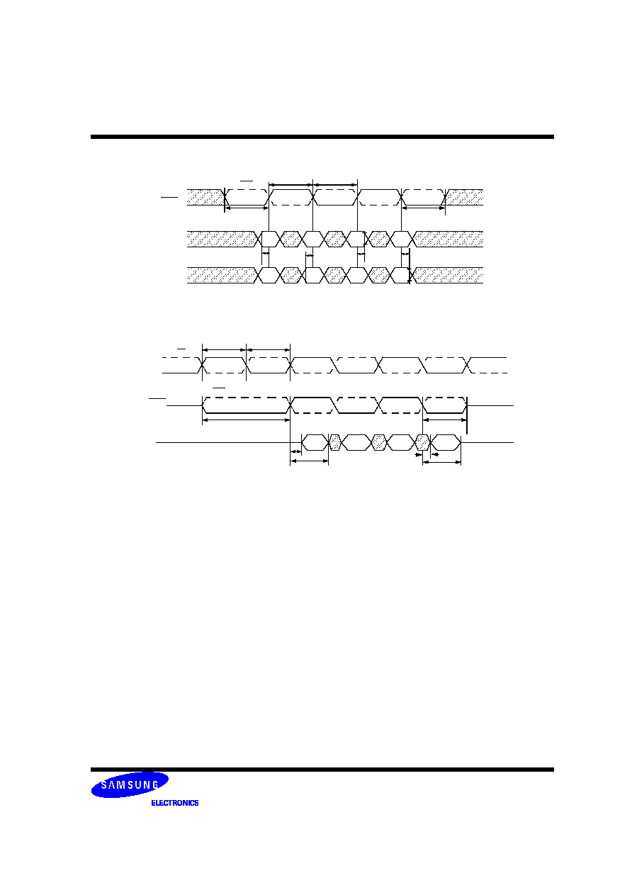
DQS
DQS
D
DMin
DQS/
DQ
DM
t
DH
Figure -- Data input (write) timing
DMin
DMin
DMin
D
D
D
DQS
V
IL
(ac)
V
IH
(ac)
V
IL
(ac)
V
IH
(ac)
V
IL
(dc)
V
IH
(dc)
V
IL
(dc)
V
IH
(dc)
t
CH
t
CL
CK
CK
CK/CK
DQS/DQS
DQ
DQS
DQS
t
RPST
Q
t
RPRE
t
DQSQmax
t
QH
t
QH
t
DQSQmax
Figure YY-- Data output (read) timing
Q
Q
Q
Page 36 of 38
512Mb B-die DDR2 SDRAM
Rev. 0.91 (Sep. 2003)
DDR2 SDRAM
Preliminary
12. A minimum of two clocks (2 * tCK) is required irrespective of operating frequency
13. Timings are guaranteed with command/address input slew rate of 1.0 V/ns. See System Derating for
other slew rate values.
14. Timings are guaranteed with data, mask, and (DQS/RDQS in singled ended mode) input slew rate of 1.0
V/ns. See System Derating for other slew rate values.
15. Timings are guaranteed with CK/CK differential slew rate of 2.0 V/ns. Timings are guaranteed for DQS
signals with a differential slew rate of 2.0 V/ns in differential strobe mode and a slew rate of 1V/ns in single
ended mode. See System Derating for other slew rate values.
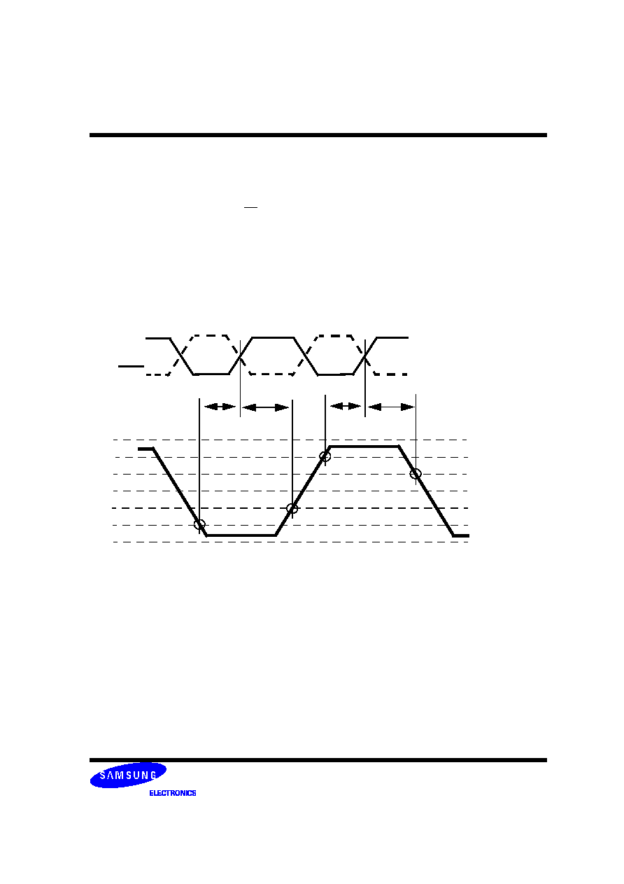
16. tDS and tDH (data setup and hold) derating
1) Input waveform timing is referenced from the input signal crossing at the V
IH(ac)
level for a rising
signal and V
IL(ac)
for a falling signal applied to the device under test.
2) Input waveform timing is referenced from the input signal crossing at the V
IH(dc)
level for a rising
signal and V
IL(dc)
for a falling signal applied to the device under test.
17. tIS and tIH (input setup and hold) derating
1) Input waveform timing is referenced from the input signal crossing at the V
IH(ac)
level for a rising
signal and V
IL(ac)
for a falling signal applied to the device under test.
2) Input waveform timing is referenced from the input signal crossing at the V
IH(dc)
level for a rising
signal and V
IL(dc)
for a falling signal applied to the device under test
tDS
V
DDQ
V
IH(ac)
min
V
IH(dc)
min
V
REF
V
IL(dc)
max
V
IL(ac)
max
V
SS
DQS
DQS
tDH
tDS
tDH
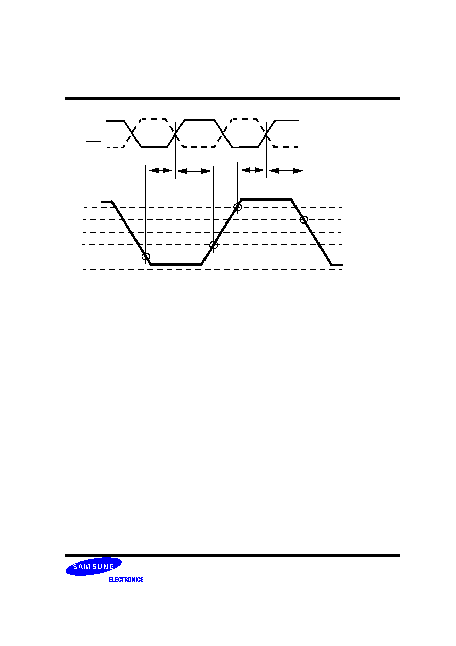
Page 37 of 38
512Mb B-die DDR2 SDRAM
Rev. 0.91 (Sep. 2003)
DDR2 SDRAM
Preliminary
18. The maximum limit for this parameter is not a device limit. The device will operate with a greater value for
this parameter, but system performance (bus turnaround) will degrade accordingly.
19. MIN ( t CL, t CH) refers to the smaller of the actual clock low time and the actual clock high time as pro-
vided to the device (i.e. this value can be greater than the minimum specification limits for t CL and t CH). For
example, t CL and t CH are = 50% of the period, less the half period jitter ( t JIT(HP)) of the clock source, and
less the half period jitter due to crosstalk ( t JIT(crosstalk)) into the clock traces.
20. t QH = t HP ≠ t QHS, where:
tHP = minimum half clock period for any given cycle and is defined by clock high or clock low ( tCH, tCL).
tQHS accounts for:
1) The pulse duration distortion of on-chip clock circuits; and
2) The worst case push-out of DQS on one transition followed by the worst case pull-in of DQ on the
next transition, both of which are, separately, due to data pin skew and output pattern effects, and p-
channel to n-channel variation of the output drivers.
21. tDQSQ: Consists of data pin skew and output pattern effects, and p-channel to n-channel variation of the
output drivers for any given cycle.
22. t DAL = (nWR) + ( tRP/tCK):
For each of the terms above, if not already an integer, round to the next highest integer. tCK refers to the
application clock period. nWR refers to the t WR parameter stored in the MRS.
Example: For DDR533 at t CK = 3.75 ns with t WR programmed to 4 clocks. tDAL = 4 + (15 ns / 3.75 ns)
clocks =4 +(4)clocks=8clocks.
23. The clock frequency is allowed to change during self≠refresh mode or precharge power-down mode. In
case of clock frequency change during precharge power-down, a specific procedure is required as described
in section 3.2.9.
tIS
V
DDQ
V
IH(ac)
min
V
IH(dc)
min
V
REF
V
IL(dc)
max
V
IL(ac)
max
V
SS
CK
CK
tIH
tIS
tIH

Page 38 of 38
512Mb B-die DDR2 SDRAM
Rev. 0.91 (Sep. 2003)
DDR2 SDRAM
Preliminary
24. ODT turn on time min is when the device leaves high impedance and ODT resistance begins to turn on.
ODT turn on time max is when the ODT resistance is fully on. Both are measured from tAOND.
25. ODT turn off time min is when the device starts to turn off ODT resistance.
ODT turn off time max is when the bus is in high impedance. Both are measured from tAOFD