
Page 1 of 27
256Mb F-die DDR2 SDRAM
Rev. 1.5 Feb. 2005
DDR2 SDRAM
256Mb F-die DDR2 SDRAM Specification
Version 1.5
February 2005

Page 2 of 27
256Mb F-die DDR2 SDRAM
Rev. 1.5 Feb. 2005
DDR2 SDRAM
Contents
0. Ordering Information
1. Key Feature
2. Package Pinout/Mechnical Dimension & Addressing
2.1 Package Pintout & Mechnical Dimension
2.2 Input/Output Function Description
2.3 Addressing
3. Absolute Maximum Rating
4. AC & DC Operating Conditions & Specifications
Page 3 of 27
256Mb F-die DDR2 SDRAM
Rev. 1.5 Feb. 2005
DDR2 SDRAM
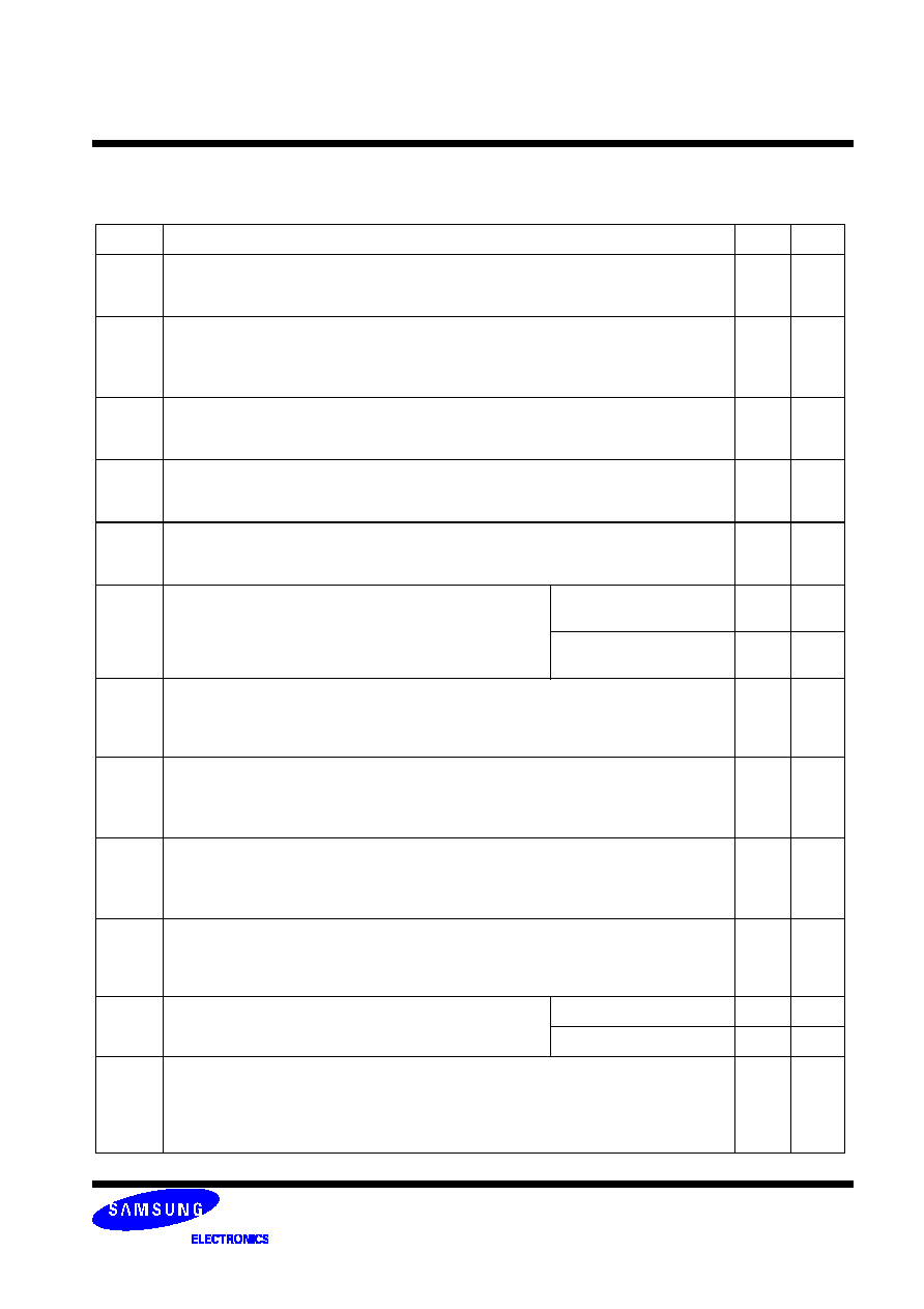
1.Key Features
Note : This data sheet is an abstract of full DDR2 specification and does not cover the common features
which are described in "Samsung's DDR2 SDRAM Device Operation & Timing Diagram"
Speed
DDR2-667
5-5-5
DDR2-533
4-4-4
DDR2-400
3-3-3
Units
CAS Latency
5
4
3
tCK
tRCD(min)
15
15
15
ns
tRP(min)
15
15
15
ns
tRC(min)
54
55
55
ns
� JEDEC standard 1.8V � 0.1V Power Supply
� VDDQ = 1.8V � 0.1V
� 200 MHz f
CK
for 400Mb/sec/pin, 267MHz f
CK
for
533Mb/sec/pin, 333MHz f
CK
for 667Mb/sec/pin
� 4 Banks
� Posted CAS
� Programmable CAS Latency: 3, 4, 5
� Programmable Additive Latency: 0, 1 , 2 , 3 and 4
� Write Latency(WL) = Read Latency(RL) -1
� Burst Length: 4 , 8(Interleave/nibble sequential)
� Programmable Sequential / Interleave Burst Mode
� Bi-directional Differential Data-Strobe (Single-ended
data-strobe is an optional feature)
� Off-Chip Driver(OCD) Impedance Adjustment
� On Die Termination
� Average Refesh Period 7.8us at lower then T
CASE
85
�C,
3.9us at 85
�C < T
CASE
< 95
�C
� Package: 60ball FBGA - 64Mx4/32Mx8
� All of Lead-free products are compliant for RoHS
The 256Mb DDR2 SDRAM chip is organized as either
16Mbit x 4 I/Os x 4 banks or 8Mbit x 8 I/Os x 4banks
device. This synchronous device achieves high speed dou-
ble-data-rate transfer rates of up to 667Mb/sec/pin (DDR2-
667) for general applications.
The chip is designed to comply with the following key
DDR2 SDRAM features such as posted CAS with additive
latency, write latency = read latency - 1, Off-Chip
Driver(OCD) impedance adjustment and On Die Termina-
tion.
All of the control and address inputs are synchronized with
a pair of externally supplied differential clocks. Inputs are
latched at the crosspoint of differential clocks (CK rising
and CK falling). All I/Os are synchronized with a pair of
bidirectional strobes (DQS and DQS) in a source synchro-
nous fashion. The address bus is used to convey row, col-
umn, and bank address information in a RAS/CAS
multiplexing style. For example, 256Mb(x4) device receive
13/11/2 addressing.
The 256Mb DDR2 device operates with a single
1.8V � 0.1V power supply and 1.8V � 0.1V VDDQ.
The 256Mb DDR2 device is available in 60ball
FBGAs(x4/x8).
Note: The functionality described and the timing specifica-
tions included in this data sheet are for the DLL Enabled
mode of operation.
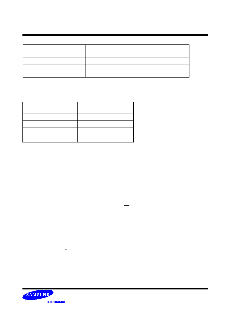
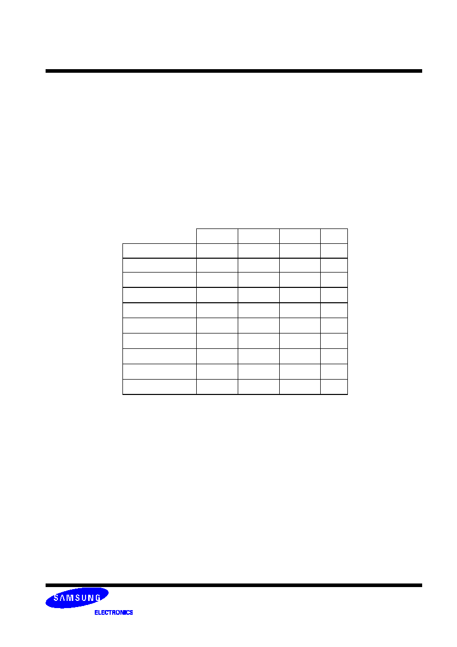
0. Ordering Information
Note: Speed bin is in order of CL-tRCD-tRP
Organization
DDR2-667 5-5-5
DDR2-533 4-4-4
DDR2-400 3-3-3
Package
64Mx4
-
K4T56043QF-GCD5
K4T56043QF-GCCC
Leaded
64Mx4
-
K4T56043QF-ZCD5
K4T56043QF-ZCCC
Lead-free
32Mx8
K4T56083QF-GCE6
K4T56083QF-GCD5
K4T56083QF-GCCC
Leaded
32Mx8
K4T56083QF-ZCE6
K4T56083QF-ZCD5
K4T56083QF-ZCCC
Lead-free
Page 4 of 27
256Mb F-die DDR2 SDRAM
Rev. 1.5 Feb. 2005
DDR2 SDRAM
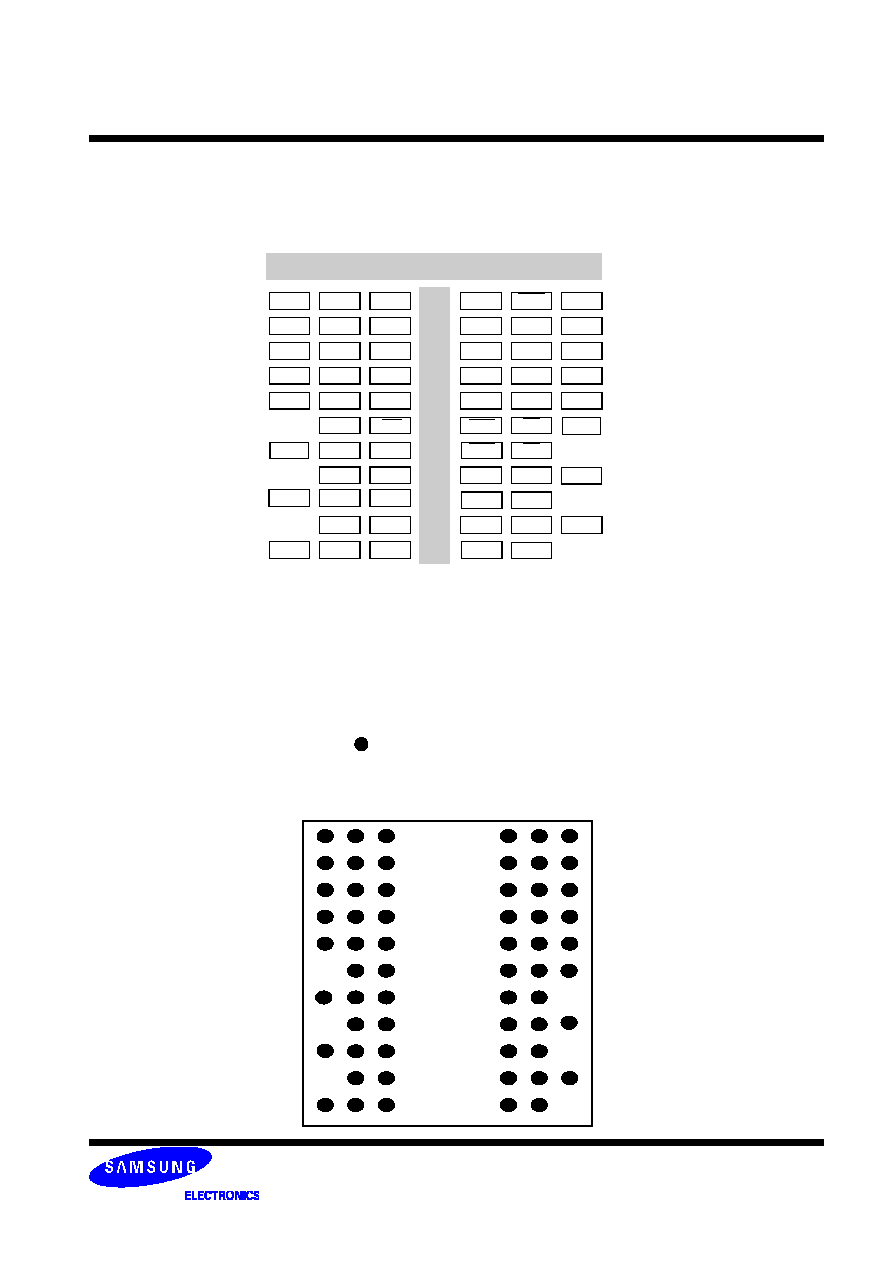
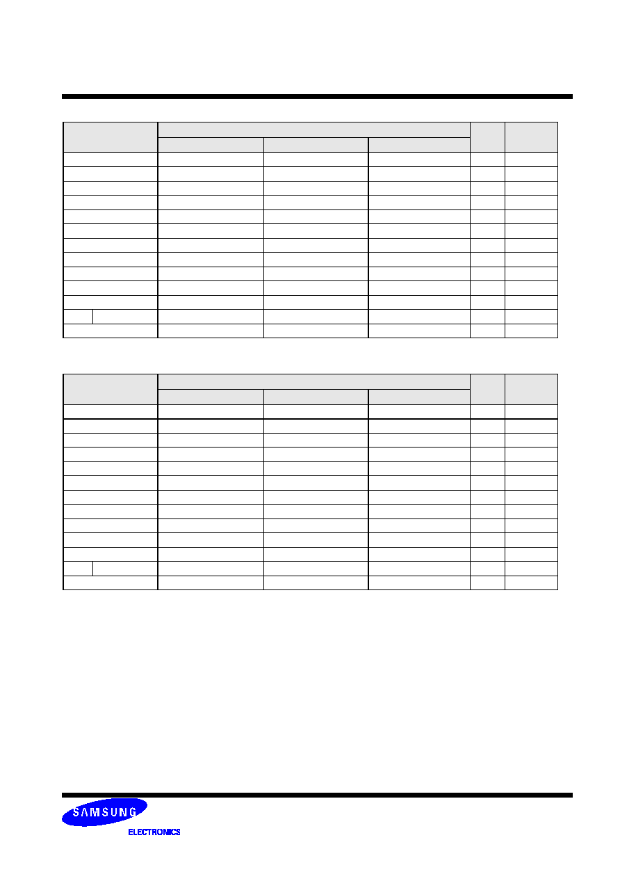
2. Package Pinout/Mechnical Dimension & Addressing
2.1 Package Pinout
x4 package pinout (Top View) : 60ball FBGA Package
Notes:
1. Pin B3 has identical capacitance as pin B7.
2. VDDL and VSSDL are power and ground for the DLL.
A
B
C
D
E
F
G
H
J
K
L
VDD
NC
VSS
NC
VSSQ
DM
VDDQ
VDDQ
VDDQ
VSSQ
VSSQ
DQS
DQS
NC
DQ0
VDDQ
DQ2
VSSQ
NC
VSSDL
VDD
CK
RAS
CK
CAS
CS
A2
A6
A4
A11
A8
NC
NC
NC
A12
A9
A7
A5
A0
VDD
A10
VSS
VDDQ
VSSQ
DQ1
DQ3
NC
VDDL
A1
A3
BA1
VREF
VSS
CKE
WE
BA0
VDD
VSS
ODT
NC
+
+
+
+
+
+
+
+
+
+
+
+
+
+
+
+
+
+
+
+
+
+
+
+
+
+
+
+
+
+
+
+
+
+
+
+
+
+
+
+
1
2
3
4
5
6
7
8
9
A
B
C
D
E
F
G
H
J
K
L
Ball Locations (x4)
: Populated Ball
+ : Depopulated Ball
Top View (See the balls through the Package)
9
1
2
3
7
8
Page 5 of 27
256Mb F-die DDR2 SDRAM
Rev. 1.5 Feb. 2005
DDR2 SDRAM
Notes:
1.
Pins B3 and A2 have identical capacitance as pins B7 and A8.
2.
For a read, when enabled, strobe pair RDQS & RDQS are identical in function and timing to strobe pair DQS
& DQS and input masking function is disabled.
3.
The function of DM or RDQS/RDQS are enabled by EMRS command.
4.
VDDL and VSSDL are power and ground for the DLL.
x8 package pinout (Top View) : 60ball FBGA Package
A
B
C
D
E
F
G
H
J
K
L
VDD
NU/
VSS
DQ6
VSSQ
VDDQ
VDDQ
VDDQ
VSSQ
VSSQ
DQS
DQS
DQ7
DQ0
VDDQ
DQ2
VSSQ
DQ5
VSSDL
VDD
CK
RAS
CK
CAS
CS
A2
A6
A4
A11
A8
NC
NC
NC
A12
A9
A7
A5
A0
VDD
A10
VSS
VDDQ
VSSQ
DQ1
DQ3
DQ4
VDDL
A1
A3
BA1
VREF
VSS
CKE
WE
BA0
VDD
VSS
DM/
RDQS
RDQS
NC
ODT
+
+
+
+
+
+
+
+
+
+
+
+
+
+
+
+
+
+
+
+
+
+
+
+
+
+
+
+
+
+
+
+
+
+
+
+
+
1
2
3
4
5
6
7
8
9
A
B
C
D
E
F
G
H
J
K
L
+
+
Ball Locations (x8)
: Populated Ball
+ : Depopulated Ball
Top View (See the balls through the Package)
9
1
2
3
7
8
Page 6 of 27
256Mb F-die DDR2 SDRAM
Rev. 1.5 Feb. 2005
DDR2 SDRAM
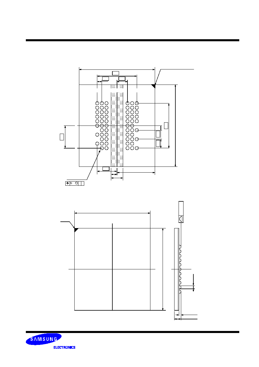
FBGA Package Dimension(x4/x8)
13
.00
�
0.1
0
8.
0
0
0.
80
1.
60
11.00
�
0.10
1
2
3
4
5
6
7
8
9
6.40
0.80
1.60
B
C
D
E
F
G
H
J
K
L
A
4.
00
(5.50)
(0.90)
(1.80)
3.20
60-
0.45
�
0.05
0.2 M A B
13
.0
0
�
0.1
0
11.00
�
0.10
0.4
5
�
0.
0
5
0.
1
0
MA
X
0.35
�
0.05
MAX.1.20
# A1 INDEX MARK
#A1
Page 7 of 27
256Mb F-die DDR2 SDRAM
Rev. 1.5 Feb. 2005
DDR2 SDRAM
2.2 Input/Output Functional Description
Symbol
Type
Function
CK, CK
Input
Clock: CK and CK are differential clock inputs. All address and control input signals are sampled
on the crossing of the positive edge of CK and negative edge of CK. Output (read) data is refer-
enced to the crossings of CK and CK (both directions of crossing).
CKE
Input
Clock Enable: CKE HIGH activates, and CKE Low deactivates, internal clock signals and device
input buffers and output drivers. Taking CKE Low provides Precharge Power-Down and Self
Refresh operation (all banks idle), or Active Power-Down (row Active in any bank). CKE is syn-
chronous for power down entry and exit, and for self refresh entry. CKE is asynchronous for self
refresh exit. After V
REF
has become stable during the power on and initialization swquence, it
must be maintained for proper operation of the CKE receiver. For proper self-refresh entry and
exit, V
REF
must be maintained to this input. CKE must be maintained high throughout read and
write accesses. Input buffers, excluding CK, CK, ODT and CKE are disabled during power-down.
Input buffers, excluding CKE, are disabled during self refresh.
CS
Input
Chip Select: All commands are masked when CS is registered HIGH. CS provides for external
Rank selection on systems with multiple Ranks. CS is considered part of the command code.
ODT
Input
On Die Termination: ODT (registered HIGH) enables termination resistance internal to the DDR2
SDRAM. When enabled, ODT is only applied to each DQ, DQS, DQS, RDQS, RDQS, and DM
signal for x4/x8 configurations. The ODT pin will be ignored if the Extended Mode Register
Set(EMRS) is programmed to disable ODT.
RAS, CAS, WE
Input
Command Inputs: RAS, CAS and WE (along with CS) define the command being entered.
DM
Input
Input Data Mask: DM is an input mask signal for write data. Input data is masked when DM is
sampled HIGH coincident with that input data during a Write access. DM is sampled on both
edges of DQS. Although DM pins are input only, the DM loading matches the DQ and DQS load-
ing. For x8 device, the function of DM or RDQS/RDQS is enabled by EMRS command.
BA0 - BA1
Input
Bank Address Inputs: BA0 and BA1 define to which bank an Active, Read, Write or Precharge
command is being applied. Bank address also determines if the mode register or extended mode
register is to be accessed during a MRS or EMRS cycle.
A0 - A12
Input
Address Inputs: Provided the row address for Active commands and the column address and
Auto Precharge bit for Read/Write commands to select one location out of the memory array in the
respective bank. A10 is sampled during a Precharge command to determine whether the Pre-
charge applies to one bank (A10 LOW) or all banks (A10 HIGH). If only one bank is to be pre-
charged, the bank is selected by BA0, BA1. The address inputs also provide the op-code during
Mode Register Set commands.
DQ
Input/Output Data Input/ Output: Bi-directional data bus.
DQS, (DQS)
(RDQS), (RDQS)
Input/Output
Data Strobe: output with read data, input with write data. Edge-aligned with read data, centered in
write data. For the x8, an RDQS option using DM pin can be enabled via the EMRS(1) to simplify
read timing. The data strobes DQS and RDQS may be used in single ended mode or paired with
optional complementary signals DQS and RDQS to provide differential pair signaling to the system
during both reads and writes. An EMRS(1) control bit enables or disables all complementary data
strobe signals.
NC
No Connect: No internal electrical connection is present.
V
DD
/V
DDQ
Supply
Power Supply: 1.8V +/- 0.1V, DQ Power Supply: 1.8V +/- 0.1V
V
SS
/V
SSQ
Supply
Ground, DQ Ground
V
DDL
Supply
DLL Power Supply: 1.8V +/- 0.1V
V
SSDL
Supply
DLL Ground
V
REF
Supply
Reference voltage
In this data sheet, "differential DQS signals" refers to any of the following with A10 = 0 of EMRS(1)
x4 DQS/DQS
x8
DQS/DQS
if EMRS(1)[A11] = 0
x8 DQS/DQS, RDQS/RDQS,
if EMRS(1)[A11] = 1
"single-ended DQS signals" refers to any of the following with A10 = 1 of EMRS(1)
x4
DQS
x8 DQS
if EMRS(1) [A11] = 0
x8 DQS, RDQS, if EMRS(1) [A11] = 1

Page 8 of 27
256Mb F-die DDR2 SDRAM
Rev. 1.5 Feb. 2005
DDR2 SDRAM
2.3 256Mb Addressing
* Reference information: The following tables are address mapping information for other densities.
512Mb
1Gb
2Gb
4Gb
Configuration
64Mb x4
32Mb x 8
# of Bank
4
4
Bank Address
BA0,BA1
BA0,BA1
Auto precharge
A
10
/AP
A
10
/AP
Row Address
A
0
~ A
12
A
0
~ A
12
Column Address
A
0
~ A
9,
A
11
A
0
~ A
9
Configuration
128Mb x4
64Mb x 8
32Mb x16
# of Bank
4
4
4
Bank Address
BA0,BA1
BA0,BA1
BA0,BA1
Auto precharge
A
10
/AP
A
10
/AP
A
10
/AP
Row Address
A
0
~ A
13
A
0
~ A
13
A
0
~ A
12
Column Address
A
0
~ A
9,
A
11
A
0
~ A
9
A
0
~ A
9
Configuration
256Mb x4
128Mb x 8
64Mb x16
# of Bank
8
8
8
Bank Address
BA0 ~ BA2
BA0 ~ BA2
BA0 ~ BA2
Auto precharge
A
10
/AP
A
10
/AP
A
10
/AP
Row Address
A
0
~ A
13
A
0
~ A
13
A
0
~ A
12
Column Address
A
0
~ A
9,
A
11
A
0
~ A
9
A
0
~ A
9
Configuration
512Mb x4
256Mb x 8
128Mb x16
# of Bank
8
8
8
Bank Address
BA0 ~ BA2
BA0 ~ BA2
BA0 ~ BA2
Auto precharge
A
10
/AP
A
10
/AP
A
10
/AP
Row Address
A
0
~ A
14
A
0
~ A
14
A
0
~ A
13
Column Address
A
0
~ A
9,
A
11
A
0
~ A
9
A
0
~ A
9
Configuration
1 Gb x4
512Mb x 8
256Mb x16
# of Bank
8
8
8
Bank Address
BA0 ~ BA2
BA0 ~ BA2
BA0 ~ BA2
Auto precharge
A
10
/AP
A
10
/AP
A
10
/AP
Row Address
A
0
- A
15
A
0
- A
15
A
0
- A
14
Column Address/page size
A
0
- A
9,
A
11
A
0
- A
9
A
0
- A
9

Page 9 of 27
256Mb F-die DDR2 SDRAM
Rev. 1.5 Feb. 2005
DDR2 SDRAM
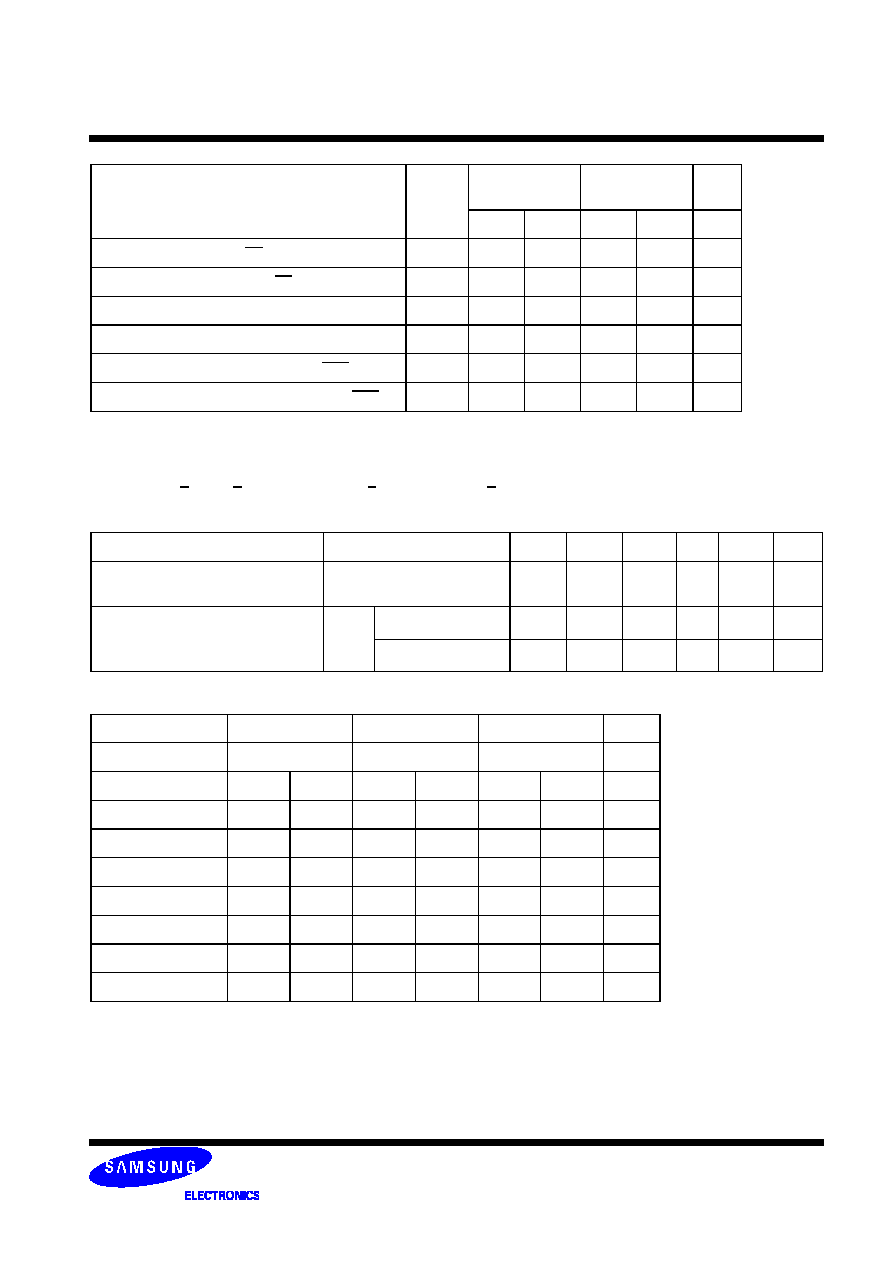
3. Absolute Maximum DC Ratings
4. AC & DC Operating Conditions
Recommended DC Operating Conditions (SSTL - 1.8)
Symbol
Parameter Rating
Units
Notes
VDD
Voltage on VDD pin relative to Vss
- 1.0 V ~ 2.3 V
V
1
VDDQ
Voltage on VDDQ pin relative to Vss
- 0.5 V ~ 2.3 V
V
1
VDDL
Voltage on VDDL pin relative to Vss
- 0.5 V ~ 2.3 V
V
1
V
IN
,
V
OUT
Voltage on any pin relative to Vss
- 0.5 V ~ 2.3 V
V
1
T
STG
Storage Temperature
-55 to +100
�C 1,
2
1.
Stresses greater than those listed under "Absolute Maximum Ratings" may cause permanent damage to the device. This is a
stress rating only and functional operation of the device at these or any other conditions above those indicated in the operational
sections of this specification is not implied. Exposure to absolute maximum rating conditions for extended periods may affect reli-
ability.
2. Storage Temperature is the case surface temperature on the center/top side of the DRAM. For the measurement conditions, please
refer to JESD51-2 standard.
Symbol
Parameter
Rating
Units
Notes
Min.
Typ. Max.
VDD
Supply Voltage
1.7
1.8
1.9
V
VDDL
Supply Voltage for DLL
1.7
1.8
1.9
V
4
VDDQ
Supply Voltage for Output
1.7
1.8
1.9
V
4
VREF
Input Reference Voltage
0.49*VDDQ
0.50*VDDQ
0.51*VDDQ
mV
1,2
VTT
Termination Voltage
V
REF
-0.04
V
REF
V
REF
+0.04
V
3
There is no specific device VDD supply voltage requirement for SSTL-1.8 compliance. However under all conditions VDDQ must
be less than or equal to VDD.
1. The value of VREF may be selected by the user to provide optimum noise margin in the system. Typically the value of VREF is
expected to be about 0.5 x VDDQ of the transmitting device and VREF is expected to track variations in VDDQ.
2. Peak to peak AC noise on VREF may not exceed +/-2% VREF(DC).
3. VTT of transmitting device must track VREF of receiving device.
4. AC parameters are measured with VDD, VDDQ and VDDDL tied together.
Page 10 of 27
256Mb F-die DDR2 SDRAM
Rev. 1.5 Feb. 2005
DDR2 SDRAM
Operating Temperature Condition
1. Operating Temperature is the case surface temperature on the center/top side of the DRAM. For the measurement conditions,
please refer to JESD51.2 standard.
2. At 85 - 95
�C operation temperature range, doubling refresh commands in frequency to a 32ms period ( tREFI=3.9 us ) is required,
and to enter to self refresh mode at this temperature range, an EMRS command is required to change internal refresh rate.
Input DC Logic Level
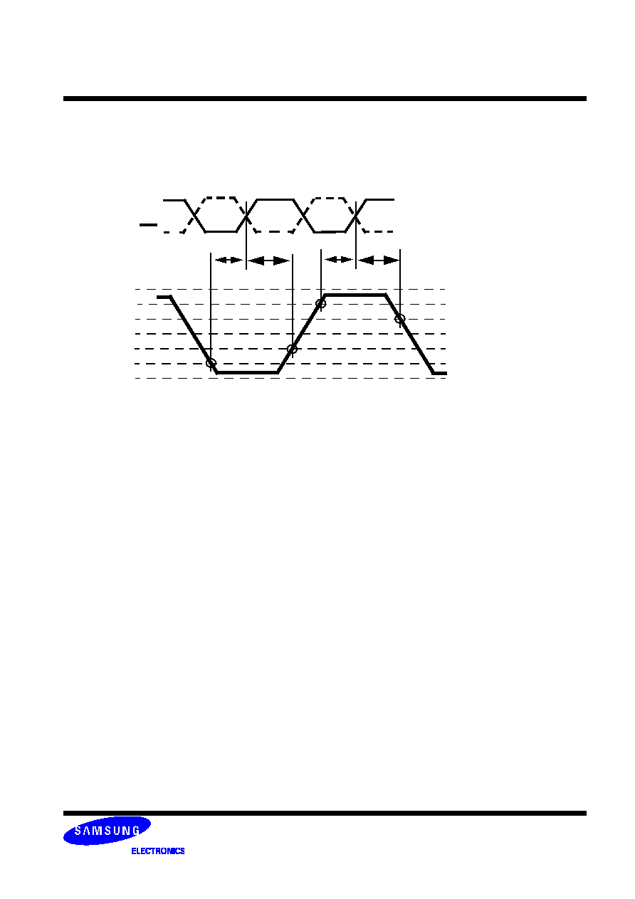
Input AC Logic Level
AC Input Test Conditions
Notes:
1.
Input waveform timing is referenced to the input signal crossing through the V
IH/IL
(AC)
level applied to the device under test.
2.
The input signal minimum slew rate is to be maintained over the range from V
REF
to V
IH
(AC) min for rising edges and the range
from V
REF
to V
IL
(AC) max for falling edges as shown in the below figure.
3.
AC timings are referenced with input waveforms switching from V
IL
(AC) to V
IH
(AC) on the positive transitions and V
IH
(AC) to
V
IL
(AC) on the negative transitions.
Symbol
Parameter
Rating
Units
Notes
TOPER
Operating Temperature
0 to 95
�C 1,
2
Symbol
Parameter
Min.
Max.
Units
Notes
V
IH
(DC)
DC input logic high
V
REF
+ 0.125
V
DDQ
+ 0.3
V
V
IL
(DC)
DC input logic low
- 0.3
V
REF
- 0.125
V
Symbol
Parameter
DDR2-400, DDR2-533
DDR2-667
Min.
Max.
Min.
Max.
V
IH
(ac)
ac input logic high
V
REF
+ 0.250
-
V
REF
+ 0.200
V
IL
(ac)
ac input logic low
-
V
REF
- 0.250
V
REF
- 0.200
Symbol
Condition
Value
Units
Notes
V
REF
Input reference voltage
0.5 * V
DDQ
V
1
V
SWING(MAX)
Input signal maximum peak to peak swing
1.0
V
1
SLEW
Input signal minimum slew rate
1.0
V/ns
2, 3
V
DDQ
V
IH
(AC) min
V
IH
(DC) min
V
REF
V
IL
(DC) max
V
IL
(AC) max
V
SS
< AC Input Test Signal Waveform >
V
SWING(MAX)
delta TR
delta TF
V
REF
- V
IL
(AC) max
delta TF
Falling Slew =
Rising Slew =
V
IH
(AC) min - V
REF
delta TR
Page 11 of 27
256Mb F-die DDR2 SDRAM
Rev. 1.5 Feb. 2005
DDR2 SDRAM
Differential input AC logic Level
Notes:
1. V
ID
(AC) specifies the input differential voltage |V
TR
-V
CP
| required for switching, where V
TR
is the true input signal (such as CK, DQS,
LDQS or UDQS) and V
CP
is the complementary input signal (such as CK, DQS, LDQS or UDQS). The minimum value is equal to V
IH
(AC)
- V
IL
(AC).
2. The typical value of V
IX
(AC) is expected to be about 0.5 * VDDQ of the transmitting device and V
IX
(AC) is expected to track variations
in VDDQ . V
IX
(AC) indicates the voltage at which differential input signals must cross.
Differential AC output parameters
Note :
1. The typical value of V
OX
(AC) is expected to be about 0.5 * VDDQ of the transmitting device and V
OX
(AC) is expected to track variations
in VDDQ . V
OX
(AC) indicates the voltage at which differential output signals must cross.
Symbol
Parameter
Min.
Max.
Units
Notes
V
ID
(AC)
AC differential input voltage
0.5
V
DDQ
+ 0.6
V
1
V
IX
(AC)
AC differential cross point voltage
0.5 * VDDQ - 0.175
0.5 * VDDQ + 0.175
V
2
Symbol
Parameter
Min.
Max.
Units
Note
V
OX
(AC)
AC differential cross point voltage
0.5 * VDDQ - 0.125
0.5 * VDDQ + 0.125
V
1
V
DDQ
Crossing point
V
SSQ
V
TR
V
CP
V
ID
V
IX or
V
OX
< Differential signal levels >
Page 12 of 27
256Mb F-die DDR2 SDRAM
Rev. 1.5 Feb. 2005
DDR2 SDRAM
OCD default characteristics
Notes:
1. Absolute Specifications (0�C
T
CASE
+95�C; VDD = +1.8V �0.1V, VDDQ = +1.8V �0.1V)
2. Impedance measurement condition for output source dc current: VDDQ = 1.7V; VOUT = 1420mV;
(VOUT-VDDQ)/Ioh must be less than 23.4 ohms for values of VOUT between VDDQ and VDDQ-
280mV. Impedance measurement condition for output sink dc current: VDDQ = 1.7V; VOUT = 280mV;
VOUT/Iol must be less than 23.4 ohms for values of VOUT between 0V and 280mV.
3. Mismatch is absolute value between pull-up and pull-dn, both are measured at same temperature and
voltage.
4. Slew rate measured from V
IL
(AC) to V
IH
(AC).
5. The absolute value of the slew rate as measured from DC to DC is equal to or greater than the slew rate as
measured from AC to AC. This is guaranteed by design and characterization.
6. This represents the step size when the OCD is near 18 ohms at nominal conditions across all process and
represents only the DRAM uncertainty.
Output slew rate load :
7. DRAM output slew rate specification applies to 400Mb/sec/pin, 533Mb/sec/pin and 667Mb/sec/pin speed
bins.
8. Timing skew due to DRAM output slew rate mis-match between DQS / DQS and associated DQs is
included in tDQSQ and tQHS specification.
Description
Parameter
Min
Nom
Max
Unit
Notes
Output impedance
12.6
18
23.4
ohms
1,2
Output impedance step
size for OCD calibration
0
1.5
ohms
6
Pull-up and pull-down
mismatch
0
4
ohms
1,2,3
Output slew rate
Sout
1.5
5
V/ns
1,4,5,6,7,8
25 ohms
V
TT
Output
(V
OUT)
Reference
Point
Page 13 of 27
256Mb F-die DDR2 SDRAM
Rev. 1.5 Feb. 2005
DDR2 SDRAM
IDD Specification Parameters and Test Conditions
(IDD values are for full operating range of Voltage and Temperature, Notes 1 - 5)
Symbol
Proposed Conditions
Units
Notes
IDD0
Operating one bank active-precharge current;
tCK = tCK(IDD), tRC = tRC(IDD), tRAS = tRASmin(IDD); CKE is HIGH, CS\ is HIGH between valid
commands; Address bus inputs are SWITCHING; Data bus inputs are SWITCHING
mA
IDD1
Operating one bank active-read-precharge current;
IOUT = 0mA; BL = 4, CL = CL(IDD), AL = 0; tCK = tCK(IDD), tRC = tRC (IDD), tRAS = tRAS-
min(IDD), tRCD = tRCD(IDD); CKE is HIGH, CS\ is HIGH between valid commands; Address busin-
puts are SWITCHING; Data pattern is same as IDD4W
mA
IDD2P
Precharge power-down current;
All banks idle; tCK = tCK(IDD); CKE is LOW; Other control and address bus inputs are STABLE;
Data bus inputs are FLOATING
mA
IDD2Q
Precharge quiet standby current;
All banks idle; tCK = tCK(IDD); CKE is HIGH, CS\ is HIGH; Other control and address bus inputs are
STABLE; Data bus inputs are FLOATING
mA
IDD2N
Precharge standby current;
All banks idle; tCK = tCK(IDD); CKE is HIGH, CS\ is HIGH; Other control and address bus inputs are
SWITCHING; Data bus inputs are SWITCHING
mA
IDD3P
Active power-down current;
All banks open; tCK = tCK(IDD); CKE is LOW; Other control and
address bus inputs are STABLE; Data bus inputs are FLOATING
Fast PDN Exit MRS(12) =
0mA
mA
Slow PDN Exit MRS(12) =
1mA
mA
IDD3N
Active standby current;
All banks open; tCK = tCK(IDD), tRAS = tRASmax(IDD), tRP = tRP(IDD); CKE is HIGH, CS\ is HIGH
between valid commands; Other control and address bus inputs are SWITCHING; Data bus inputs
are SWITCHING
mA
IDD4W
Operating burst write current;
All banks open, Continuous burst writes; BL = 4, CL = CL(IDD), AL = 0; tCK = tCK(IDD), tRAS =
tRASmax(IDD), tRP = tRP(IDD); CKE is HIGH, CS\ is HIGH between valid commands; Address bus
inputs are SWITCHING; Data bus inputs are SWITCHING
mA
IDD4R
Operating burst read current;
All banks open, Continuous burst reads, IOUT = 0mA; BL = 4, CL = CL(IDD), AL = 0; tCK =
tCK(IDD), tRAS = tRASmax(IDD), tRP = tRP(IDD); CKE is HIGH, CS\ is HIGH between valid com-
mands; Address bus inputs are SWITCHING; Data pattern is same as IDD4W
mA
IDD5B
Burst auto refresh current;
tCK = tCK(IDD); Refresh command at every tRFC(IDD) interval; CKE is HIGH, CS\ is HIGH between
valid commands; Other control and address bus inputs are SWITCHING; Data bus inputs are
SWITCHING
mA
IDD6
Self refresh current;
CK and CK\ at 0V; CKE
0.2V; Other control and address bus
inputs are FLOATING; Data bus inputs are FLOATING
Normal
mA
Low Power
mA
IDD7
Operating bank interleave read current;
All bank interleaving reads, IOUT = 0mA; BL = 4, CL = CL(IDD), AL = tRCD(IDD)-1*tCK(IDD); tCK =
tCK(IDD), tRC = tRC(IDD), tRRD = tRRD(IDD), tRCD = 1*tCK(IDD); CKE is HIGH, CS\ is HIGH
between valid commands; Address bus inputs are STABLE during DESELECTs; Data pattern is
same as IDD4R; Refer to the following page for detailed timing conditions
mA
Page 14 of 27
256Mb F-die DDR2 SDRAM
Rev. 1.5 Feb. 2005
DDR2 SDRAM
Notes:
1. IDD specifications are tested after the device is properly initialized
2. Input slew rate is specified by AC Parametric Test Condition
3. IDD parameters are specified with ODT disabled.
4. Data bus consists of DQ, DM, DQS, DQS\, RDQS, RDQS\, LDQS, LDQS\, UDQS, and UDQS\. IDD values must be met with all combi-
nations of EMRS bits 10 and 11.
5. Definitions for IDD
LOW is defined as Vin
VILAC(max)
HIGH is defined as Vin
VIHAC(min)
STABLE is defined as inputs stable at a HIGH or LOW level
FLOATING is defined as inputs at VREF = VDDQ/2
SWITCHING is defined as:
inputs changing between HIGH and LOW every other clock cycle (once per two clocks) for address and control
signals, and
inputs changing between HIGH and LOW every other data transfer (once per clock) for DQ signals not including
masks or strobes.
For purposes of IDD testing, the following parameters are utilized
Detailed IDD7
The detailed timings are shown below for IDD7.
Legend: A = Active; RA = Read with Autoprecharge; D = Deselect
IDD7: Operating Current: All Bank Interleave Read operation
All banks are being interleaved at minimum tRC(IDD) without violating tRRD(IDD) using a burst length of 4. Control and address bus
inputs are STABLE during DESELECTs. IOUT = 0mA
Timing Patterns for 4 bank devices x4/ x8/ x16
-DDR2-400 3/3/3
A0 RA0 A1 RA1 A2 RA2 A3 RA3 D D D
-DDR2-533 4/4/4
A0 RA0 D A1 RA1 D A2 RA2 D A3 RA3 D D D D D
-DDR2-667 5/5/5
A0 RA0 D D A1 RA1 D D A2 RA2 D D A3 RA3 D D D D D D
DDR2-667
DDR2-533
DDR2-400
Parameter
5-5-5
4-4-4
3-3-3
Units
CL(IDD)
5
4
3
tCK
tRCD(IDD)
15
15
15
ns
tRC(IDD)
60
60
55
ns
tRRD(IDD)-x4/x8
7.5
7.5
7.5
ns
tRRD(IDD)-x16
10
10
10
ns
tCK(IDD)
3
3.75
5
ns
tRASmin(IDD)
45
45
40
ns
tRP(IDD)
15
15
15
ns
tRFC(IDD)
105
105
105
ns
Page 15 of 27
256Mb F-die DDR2 SDRAM
Rev. 1.5 Feb. 2005
DDR2 SDRAM
DDR2 SDRAM IDD Spec Table
Symbol
64Mx4(K4T56043QF)
Unit
Notes
-
D5(DDR2-533@CL=4) CC(DDR2-400@CL=3)
IDD0
-
100
95
mA
IDD1
-
110
100
mA
IDD2P
-
8
8
mA
IDD2Q
-
25
25
mA
IDD2N
-
30
30
mA
IDD3P-F
-
30
30
mA
IDD3P-S
-
15
15
mA
IDD3N
-
70
65
mA
IDD4W
-
160
125
mA
IDD4R
-
150
125
mA
IDD5B
-
165
160
mA
IDD6
Normal
-
5
5
mA
IDD7
-
250
245
mA
Symbol
32Mx8(K4T56083QF)
Unit
Notes
E6(DDR2-667@CL=5) D5(DDR2-533@CL=4) CC(DDR2-400@CL=3)
IDD0
105
100
95
mA
IDD1
115
110
100
mA
IDD2P
8
8
8
mA
IDD2Q
30
25
25
mA
IDD2N
35
30
30
mA
IDD3P-F
35
30
30
mA
IDD3P-S
15
15
15
mA
IDD3N
75
70
65
mA
IDD4W
210
175
135
mA
IDD4R
185
160
130
mA
IDD5B
170
165
160
mA
IDD6
Normal
5
5
5
mA
IDD7
265
255
255
mA
Page 16 of 27
256Mb F-die DDR2 SDRAM
Rev. 1.5 Feb. 2005
DDR2 SDRAM
Input/Output capacitance
Electrical Characteristics & AC Timing for DDR2-667/533/400
(0
�C < T
CASE
< 95
�C; V
DDQ
= 1.8V + 0.1V; V
DD
= 1.8V + 0.1V)
Refresh Parameters by Device Density
Speed Bins and CL, tRCD, tRP, tRC and tRAS for Corresponding Bin
Parameter
Symbol
DDR2-400
DDR2-533
DDR2-667
Min
Max
Min
Max
Units
Input capacitance, CK and CK
CCK
1.0
2.0
1.0
2.0
pF
Input capacitance delta, CK and CK
CDCK
x
0.25
x
0.25
pF
Input capacitance, all other input-only pins
CI
1.0
2.0
1.0
2.0
pF
Input capacitance delta, all other input-only pins
CDI
x
0.25
x
0.25
pF
Input/output capacitance, DQ, DM, DQS, DQS
CIO
2.5
4.0
2.5
3.5
pF
Input/output capacitance delta, DQ, DM, DQS, DQS
CDIO
x
0.5
x
0.5
pF
Parameter
Symbol
256Mb
512Mb
1Gb
2Gb
4Gb
Units
Refresh to active/Refresh command
time
tRFC
75
105
127.5
195
327.5
ns
Average periodic refresh interval
tREFI
0
�C T
CASE
85�C
7.8
7.8
7.8
7.8
7.8
�s
85
�C < T
CASE
95�C
3.9
3.9
3.9
3.9
3.9
�s
Speed
DDR2-667(E6)
DDR2-533(D5)
DDR2-400(CC)
Units
Bin (CL - tRCD - tRP)
5 - 5- 5
4 - 4 - 4
3 - 3 - 3
Parameter
min
max
min
max
min
max
tCK, CL=3
5
8
5
8
5
8
ns
tCK, CL=4
3.75
8
3.75
8
5
8
ns
tCK, CL=5
3
8
-
-
-
-
ns
tRCD
15
15
15
ns
tRP
15
15
15
ns
tRC
54
55
55
ns
tRAS
39
70000
40
70000
40
70000
ns
Page 17 of 27
256Mb F-die DDR2 SDRAM
Rev. 1.5 Feb. 2005
DDR2 SDRAM
Timing Parameters by Speed Grade
(Refer to notes for informations related to this table at the bottom)
Parameter
Symbol
DDR2-667
DDR2-533
DDR2-400
Units
Notes
min
max
min
max
min
max
DQ output access time
from CK/CK
tAC
-450
+450
-500
+500
-600
+600
ps
DQS output access
time from CK/CK
tDQSCK
-400
+400
-450
+450
-500
+500
ps
CK high-level width
tCH
0.45
0.55
0.45
0.55
0.45
0.55
tCK
CK low-level width
tCL
0.45
0.55
0.45
0.55
0.45
0.55
tCK
CK half period
tHP
min(tCL
, tCH)
x
min(tCL
, tCH)
x
min(tCL
, tCH)
x
ps
20,21
Clock cycle time, CL=x
tCK
3000
8000
3750
8000
5000
8000
ps
24
DQ and DM input hold
time
tDH(base)
175
x
225
x
275
x
ps
15,16,
17,20
DQ and DM input
setup time
tDS(base)
100
x
100
x
150
x
ps
15,16,
17,21
Control & Address
input pulse width for
each input
tIPW
0.6
x
0.6
x
0.6
x
tCK
DQ and DM input
pulse width for each
input
tDIPW
0.35
x
0.35
x
0.35
x
tCK
Data-out high-
impedance time from
CK/CK
tHZ
x
tAC
max
x
tAC
max
x
tAC
max
ps
DQS low-impedance
time from CK/CK
tLZ(DQS)
tAC
min
tAC
max
tAC
min
tAC
max
tAC
min
tAC
max
ps
27
DQ low-impedance
time from CK/CK
tLZ(DQ)
2*tAC
min
tAC
max
2* tAC
min
tAC
max
2* tAC
min
tAC
max
ps
27
DQS-DQ skew for
DQS and associated
DQ signals
tDQSQ
x
240
x
300
x
350
ps
22
DQ hold skew factor
tQHS
x
340
x
400
x
450
ps
21
DQ/DQS output hold
time from DQS
tQH
tHP -
tQHS
x
tHP -
tQHS
x
tHP -
tQHS
x
ps
First DQS latching
transition to associated
clock edge
tDQSS
-0.25
0.25
-0.25
0.25
-0.25
0.25
tCK
DQS input high pulse
width
tDQSH
0.35
x
0.35
x
0.35
x
tCK
DQS input low pulse
width
tDQSL
0.35
x
0.35
x
0.35
x
tCK
DQS falling edge to
CK setup time
tDSS
0.2
x
0.2
x
0.2
x
tCK
DQS falling edge hold
time from CK
tDSH
0.2
x
0.2
x
0.2
x
tCK
Page 18 of 27
256Mb F-die DDR2 SDRAM
Rev. 1.5 Feb. 2005
DDR2 SDRAM
Parameter
Symbol
DDR2-667
DDR2-533
DDR2-400
Units
Notes
min
max
min
max
min
max
Mode register set
command cycle time
tMRD
2
x
2
x
2
x
tCK
Write postamble
tWPST
0.4
0.6
0.4
0.6
0.4
0.6
tCK
19
Write preamble
tWPRE
0.35
x
0.35
x
0.35
x
tCK
Address and control
input hold time
tIH(base)
275
x
375
x
475
x
ps
14,16,
18,23
Address and control
input setup time
tIS(base)
200
x
250
x
350
x
ps
14,16,
18,22
Read preamble
tRPRE
0.9
1.1
0.9
1.1
0.9
1.1
tCK
28
Read postamble
tRPST
0.4
0.6
0.4
0.6
0.4
0.6
tCK
28
Active to active
command period for
1KB page size
products
tRRD
7.5
x
7.5
x
7.5
x
ns
12
Active to active
command period for
2KB page size
products
tRRD
10
x
10
x
10
x
ns
12
Four Activate Window
for 1KB page size
products
tFAW
37.5
37.5
37.5
ns
Four Activate Window
for 2KB page size
products
tFAW
50
50
50
ns
CAS to CAS command
delay
tCCD
2
2
2
tCK
Write recovery time
tWR
15
x
15
x
15
x
ns
Auto precharge write
recovery + precharge
time
tDAL
WR+tR
P
x
WR+tR
P
x
WR+tR
P
x
tCK
23
Internal write to read
command delay
tWTR
7.5
x
7.5
x
10
x
ns
33
Internal read to
precharge command
delay
tRTP
7.5
7.5
7.5
ns
11
Exit self refresh to a
non-read command
tXSNR
tRFC +
10
tRFC +
10
tRFC +
10
ns
Exit self refresh to a
read command
tXSRD
200
200
200
tCK
Exit precharge power
down to any non-read
command
tXP
2
x
2
x
2
x
tCK
Exit active power down
to read command
tXARD
2
x
2
x
2
x
tCK
9

Page 19 of 27
256Mb F-die DDR2 SDRAM
Rev. 1.5 Feb. 2005
DDR2 SDRAM
Parameter
Symbol
DDR2-667
DDR2-533
DDR2-400
Units
Notes
min
max
min
max
min
max
Exit active power down
to read command
(slow exit, lower
power)
tXARDS
7 - AL
6 - AL
6 - AL
tCK
9, 10
CKE minimum pulse
width
(high and low pulse
width)
t
CKE
3
3
3
tCK
36
ODT turn-on delay
t
AOND
2
2
2
2
2
2
tCK
ODT turn-on
t
AON
tAC(mi
n)
tAC(m
ax)+0.
7
tAC(mi
n)
tAC(m
ax)+1
tAC(mi
n)
tAC(ma
x)+1
ns
13, 25
ODT turn-on(Power-
Down mode)
t
AONPD
tAC(mi
n)+2
2tCK+t
AC(ma
x)+1
tAC(mi
n)+2
2tCK+t
AC(ma
x)+1
tAC(mi
n)+2
2tCK+t
AC
(max)+
1
ns
ODT turn-off delay
t
AOFD
2.5
2.5
2.5
2.5
2.5
2.5
tCK
ODT turn-off
t
AOF
tAC(mi
n)
tAC(m
ax)+
0.6
tAC(min)
tAC(ma
x)+ 0.6
tAC(mi
n)
tAC(max
)+ 0.6
ns
26
ODT turn-off (Power-
Down mode)
t
AOFPD
tAC(mi
n)+2
2.5tCK
+tAC(
max)+
1
tAC(mi
n)+2
2.5tCK
+
tAC(m
ax)+1
tAC(mi
n)+2
2.5tCK
+
tAC(ma
x)+1
ns
ODT to power down
entry latency
tANPD
3
3
3
tCK
ODT power down exit
latency
tAXPD
8
8
8
tCK
OCD drive mode
output delay
tOIT
0
12
0
12
0
12
ns
Minimum time clocks
remains ON after CKE
asynchronously drops
LOW
tDelay
tIS+tCK
+tIH
tIS+tCK
+tIH
tIS+tCK
+tIH
ns
24

Page 20 of 27
256Mb F-die DDR2 SDRAM
Rev. 1.5 Feb. 2005
DDR2 SDRAM
General notes, which may apply for all AC parameters
1. Slew Rate Measurement Levels
a. Output slew rate for falling and rising edges is measured between VTT - 250 mV and VTT + 250 mV for
single ended signals. For differential signals (e.g. DQS - DQS) output slew rate is measured between
DQS - DQS = -500 mV and DQS - DQS = +500mV. Output slew rate is guaranteed by design, but is not
necessarily tested on each device.
b. Input slew rate for single ended signals is measured from dc-level to ac-level: from V
IL
(dc) to
V
IH
(ac) for rising edges and from V
IH
(dc) and V
IL
(ac) for falling edges.
For differential signals (e.g. CK - CK) slew rate for rising edges is measured from CK - CK = -250 mV to
CK - CK = +500 mV (250mV to -500 mV for falling edges).
c. VID is the magnitude of the difference between the input voltage on CK and the input voltage on CK, or
between DQS and DQS for differential strobe.
2. DDR2 SDRAM AC timing reference load
Following figure represents the timing reference load used in defining the relevant timing parameters of the
part. It is not intended to be either a precise representation of the typical system environment or a depiction of
the actual load presented by a production tester. System designers will use IBIS or other simulation tools to
correlate the timing reference load to a system environment. Manufacturers will correlate to their production
test conditions (generally a coaxial transmission line terminated at the tester electronics).
The output timing reference voltage level for single ended signals is the crosspoint with VTT. The output tim-
ing reference voltage level for differential signals is the crosspoint of the true (e.g. DQS) and the complement
(e.g. DQS) signal.
3. DDR2 SDRAM output slew rate test load
Output slew rate is characterized under the test conditions as shown in the following figure.
VDDQ
DUT
DQ
DQS
DQS
RDQS
RDQS
Output
V
TT
= V
DDQ
/2
25
Timing
reference
point
<AC Timing Reference Load>
VDDQ
DUT
DQ
DQS, DQS
RDQS, RDQS
Output
V
TT
= V
DDQ
/2
25
Test point
<Slew Rate Test Load>
Page 21 of 27
256Mb F-die DDR2 SDRAM
Rev. 1.5 Feb. 2005
DDR2 SDRAM
4. Differential data strobe
DDR2 SDRAM pin timings are specified for either single ended mode or differential mode depending on
the setting of the EMRS "Enable DQS" mode bit; timing advantages of differential mode are realized in sys-
tem design. The method by which the DDR2 SDRAM pin timings are measured is mode dependent. In single
ended mode, timing relationships are measured relative to the rising or falling edges of DQS crossing at
VREF. In differential mode, these timing relationships are measured relative to the crosspoint of DQS and its
complement, DQS. This distinction in timing methods is guaranteed by design and characterization. Note that
when differential data strobe mode is disabled via the EMRS, the complementary pin, DQS, must be tied
externally to VSS through a 20 ohm to 10 K ohm resisor to insure proper operation.
5. AC timings are for linear signal transitions.
6. These parameters guarantee device behavior, but they are not necessarily tested on each device. They
may be guaranteed by device design or tester correlation.
7. All voltages are referenced to VSS.
8. Tests for AC timing, IDD, and electrical (AC and DC) characteristics, may be conducted at nominal refer-
ence/supply voltage levels, but the related specifications and device operation are guaranteed for the full volt-
age range specified.
t
DS
t
DS
t
DH
t
WPRE
t
WPST
t
DQSH
t
DQSL
DQS
DQS
D
DMin
DQS/
DQ
DM
t
DH
<Data input (write) timing>
DMin
DMin
DMin
D
D
D
DQS
V
IL
(ac)
V
IH
(ac)
V
IL
(ac)
V
IH
(ac)
V
IL
(dc)
V
IH
(dc)
V
IL
(dc)
V
IH
(dc)
t
CH
t
CL
CK
CK
CK/CK
DQS/DQS
DQ
DQS
DQS
t
RPST
Q
t
RPRE
t
DQSQmax
t
QH
t
QH
t
DQSQmax
<Data output (read) timing>
Q
Q
Q
Page 22 of 27
256Mb F-die DDR2 SDRAM
Rev. 1.5 Feb. 2005
DDR2 SDRAM
Specific Notes for dedicated AC parameters
9. User can choose which active power down exit timing to use via MRS(bit 12). tXARD is expected to be
used for fast active power down exit timing. tXARDS is expected to be used for slow active power down exit
timing.
10. AL = Additive Latency
11. This is a minimum requirement. Minimum read to precharge timing is AL + BL/2 providing the tRTP and
tRAS(min) have been satisfied.
12. A minimum of two clocks (2 * tCK) is required irrespective of operating frequency
13. Timings are guaranteed with command/address input slew rate of 1.0 V/ns.
14. These parameters guarantee device behavior, but they are not necessarily tested on each device. They
may be guaranteed by device design or tester correlation.
15. Timings are guaranteed with data, mask, and (DQS/RDQS in singled ended mode) input slew rate of 1.0
V/ns.
16. Timings are guaranteed with CK/CK differential slew rate of 2.0 V/ns. Timings are guaranteed for DQS
signals with a differential slew rate of 2.0 V/ns in differential strobe mode and a slew rate of 1V/ns in single
ended mode.
17. tDS and tDH derating for DDR2-400 and DDR2-533
For all input signals the total tDS (setup time) and tDH (hold time) required is calculated by adding the
datasheet tDS(base) and tDH(base) value to the delta tDS and delta tDH derating value respectively. Exam-
ple: tDS (total setup time) = tDS(base) + delta tDS.
tDS, tDH Derating Values (ALL units in `ps', Note 1 applies to entire Table)
DQS,DQS Differential Slew Rate
4.0 V/ns
3.0 V/ns
2.0 V/ns
1.8 V/ns
1.6 V/ns
1.4V/ns
1.2V/ns
1.0V/ns
0.8V/ns
tD
S
tD
H
tD
S
tD
H
tD
S
tD
H
tD
S
tD
H
tD
S
tD
H
tD
S
tD
H
tD
S
tD
H
tD
S
tD
H
tD
S
tD
H
DQ
Slew
rate
V/ns
2.0
125
45
125
45
125
45
-
-
-
-
-
-
-
-
-
-
-
-
1.5
83
21
83
21
83
21
95
33
-
-
-
-
-
-
-
-
-
-
1.0
0
0
0
0
0
0
12
12
24
24
-
-
-
-
-
-
-
-
0.9
-
-
-11
-14
-11
-14
1
-2
13
10
25
22
-
-
-
-
-
-
0.8
-
-
-
-
-25
-31
-13
-19
-1
-7
11
5
23
17
-
-
-
-
0.7
-
-
-
-
-
-
-31
-42
-19
-30
-7
-18
5
-6
17
6
-
-
0.6
-
-
-
-
-
-
-
-
-43
-59
-31
-47
-19
-35
-7
-23
5
-11
0.5
-
-
-
-
-
-
-
-
-
-
-74
-89
-62
-77
-50
-65
-38
-53
0.4
-
-
-
-
-
-
-
-
-
-
-
-
-127 -140 -115 -128 -103 -116

Page 23 of 27
256Mb F-die DDR2 SDRAM
Rev. 1.5 Feb. 2005
DDR2 SDRAM
18. tIS and tIH (input setup and hold) derating.
tIS, tIH Derating Values for DDR2-400, DDR2-533
CK,CK Differential Slew Rate
2.0 V/ns
1.5 V/ns
1.0 V/ns
tIS
tIH
tIS
tIH
tIS
tIH
Units
Notes
Com-
mand/Ad-
dress Slew
rate
(V/ns)
4.0
+187
+94
+217
+124
+247
+154
ps
1
3.5
+179
+89
+209
+119
+239
+149
ps
1
3.0
+167
+83
+197
+113
+227
+143
ps
1
2.5
+150
+75
+180
+105
+210
+135
ps
1
2.0
+125
+45
+155
+75
+185
+105
ps
1
1.5
+83
+21
+113
+51
+143
+81
ps
1
1.0
0
0
+30
+30
+60
60
ps
1
0.9
-11
-14
+19
+16
+49
+46
ps
1
0.8
-25
-31
+5
-1
+35
+29
ps
1
0.7
-43
-54
-13
-24
+17
+6
ps
1
0.6
-67
-83
-37
-53
-7
-23
ps
1
0.5
-110
-125
-80
-95
-50
-65
ps
1
0.4
-175
-188
-145
-158
-115
-128
ps
1
0.3
-285
-292
-255
-262
-225
-232
ps
1
0.25
-350
-375
-320
-345
-290
-315
ps
1
0.2
-525
-500
-495
-470
-465
-440
ps
1
0.15
-800
-708
-770
-678
-740
-648
ps
1
tIS and tIH Derating Values for DDR2-667, DDR2-800
CK,CK Differential Slew Rate
2.0 V/ns
1.5 V/ns
1.0 V/ns
tIS
tIH
tIS
tIH
tIS
tIH
Units
Notes
Com-
mand/Ad-
dress Slew
rate
(V/ns)
4.0
+150
+94
+180
+124
+210
+154
ps
1
3.5
+143
+89
+173
+119
+203
+149
ps
1
3.0
+133
+83
+163
+113
+193
+143
ps
1
2.5
+120
+75
+150
+105
+180
+135
ps
1
2.0
+100
+45
+130
+75
+160
+105
ps
1
1.5
+67
+21
+97
+51
+127
+81
ps
1
1.0
0
0
+30
+30
+60
+60
ps
1
0.9
-5
-14
+25
+16
+55
+46
ps
1
0.8
-13
-31
+17
-1
+47
+29
ps
1
0.7
-22
-54
+8
-24
+38
+6
ps
1
0.6
-34
-83
-4
-53
+26
-23
ps
1
0.5
-60
-125
-30
-95
0
-65
ps
1
0.4
-100
-188
-70
-158
-40
-128
ps
1
0.3
-168
-292
-138
-262
-108
-232
ps
1
0.25
-200
-375
-170
-345
-140
-315
ps
1
0.2
-325
-500
-295
-470
-265
-440
ps
1
0.15
-517
-708
-487
-678
-457
-648
ps
1
0.1
-1000
-1125
-970
-1095
-940
-1065
ps
1

Page 24 of 27
256Mb F-die DDR2 SDRAM
Rev. 1.5 Feb. 2005
DDR2 SDRAM
For all input signals the total tIS (setup time) and tIH (hold time) required is calculated by adding the
datasheet tIS(base) and tIH(base) value to the delta tIS and delta tIH derating value respectively. Example:
tIS (total setup time) = tIS(base) + delta tIS
19. The maximum limit for this parameter is not a device limit. The device will operate with a greater value for
this parameter, but system performance (bus turnaround) will degrade accordingly.
20. MIN ( tCL, tCH) refers to the smaller of the actual clock low time and the actual clock high time as pro-
vided to the device (i.e. this value can be greater than the minimum specification limits for tCL and tCH). For
example, tCL and tCH are = 50% of the period, less the half period jitter ( tJIT(HP)) of the clock source, and
less the half period jitter due to crosstalk ( tJIT(crosstalk)) into the clock traces.
21. tQH = tHP � tQHS, where:
tHP = minimum half clock period for any given cycle and is defined by clock high or clock low ( tCH, tCL).
tQHS accounts for:
1) The pulse duration distortion of on-chip clock circuits; and
2) The worst case push-out of DQS on one transition followed by the worst case pull-in of DQ on the
next transition, both of which are, separately, due to data pin skew and output pattern effects, and p-
channel to n-channel variation of the output drivers.
22. tDQSQ: Consists of data pin skew and output pattern effects, and p-channel to n-channel variation of the
output drivers as well as output slew rate mismatch between DQS / DQS and associated DQ in any given
cycle.
23. DAL = WR + RU{tRP(ns)/tCK(ns)}, where RU stands for round up.
WR refers to the tWR parameter stored in the MRS. For tRP, if the result of the division is not already an inte-
ger, round up to the next highest integer. tCK refers to the application clock period.
Example: For DDR533 at tCK = 3.75ns with tWR programmed to 4 clocks.
tDAL = 4 + (15 ns / 3.75 ns) clocks = 4 + (4) clocks = 8 clocks.
24. The clock frequency is allowed to change during self�refresh mode or precharge power-down mode. In
case of clock frequency change during precharge power-down, a specific procedure is required as described
in DDR2 device operation
25. ODT turn on time min is when the device leaves high impedance and ODT resistance begins to turn on.
ODT turn on time max is when the ODT resistance is fully on. Both are measured from tAOND.
26. ODT turn off time min is when the device starts to turn off ODT resistance.
ODT turn off time max is when the bus is in high impedance. Both are measured from tAOFD.
27. tHZ and tLZ transitions occur in the same access time as valid data transitions. These parameters are ref-
erenced to a specific voltage level which specifies when the device output is no longer driving (tHZ), or begins
driving (tLZ). Following figure shows a method to calculate the point when device is no longer driving (tHZ), or
begins driving (tLZ) by measuring the signal at two different voltages. The actual voltage measurement points
are not critical as long as the calculation is consistent.
28. tRPST end point and tRPRE begin point are not referenced to a specific voltage level but specify when
the device output is no longer driving (tRPST), or begins driving (tRPRE). Following figure shows a method to
calculate these points when the device is no longer driving (tRPST), or begins driving (tRPRE) by measuring
the signal at two different voltages. The actual voltage measurement points are not critical as long as the cal-

Page 25 of 27
256Mb F-die DDR2 SDRAM
Rev. 1.5 Feb. 2005
DDR2 SDRAM
culation is consistent.
These notes are referenced in the "Timing parameters by speed grade" tables for DDR2-400/533/667 and
DDR2-800.
29. Input waveform timing with differential data strobe enabled MR[bit10]=0, is referenced from the input sig-
nal crossing at the V
IH(ac)
level to the differential data strobe crosspoint for a rising signal, and from the input
signal crossing at the V
IL(ac)
level to the differential data strobe crosspoint for a falling signal applied to the
device under test.
30. Input waveform timing with differential data strobe enabled MR[bit10]=0, is referenced from the input sig-
nal crossing at the V
IH(dc)
level to the differential data strobe crosspoint for a rising signal and V
IL(dc)
to the
differential data strobe crosspoint for a falling signal applied to the device under test.
Differential Input waveform timing
tHZ
tRPST
end point
T1
T2
VOH + x mV
VOH + 2x mV
VOL + 2x mV
VOL + x mV
tLZ
tRPRE
begin point
T2
T1
VTT + 2x mV
VTT + x mV
VTT - x mV
VTT - 2x mV
tLZ,tRPRE
begin point
= 2*T1-T2
tHZ,tRPST
end point
= 2*T1-T2
<Test method for tLZ, tHZ, tRPRE and tRPST>
tDS
V
DDQ
V
IH(ac)
min
V
IH(dc)
min
V
REF(dc)
V
IL(dc)
max
V
IL(ac)
max
V
SS
DQS
DQS
tDH
tDS
tDH
Page 26 of 27
256Mb F-die DDR2 SDRAM
Rev. 1.5 Feb. 2005
DDR2 SDRAM
31. Input waveform timing is referenced from the input signal crossing at the V
IH(ac)
level for a rising signal and V
IL(ac)
for a falling signal applied to the device under test.
32. Input waveform timing is referenced from the input signal crossing at the V
IH(dc)
level for a rising signal and V
IL(dc)
for a falling signal applied to the device under test.
33. tWTR is at lease two clocks (2 * tCK) independent of operation frequency.
34. Input waveform timing with single-ended data strobe enabled MR[bit10] = 1, is referenced from the input
signal crossing at the VIH(ac) level to the single-ended data strobe crossing VIH/L(dc) at the start of its tran-
sition for a rising signal, and from the input signal crossing at the VIL(ac) level to the single-ended data strobe
crossing VIH/L(dc) at the start of its transition for a falling signal applied to the device under test. The DQS
signal must be monotonic between Vil(dc)max and Vih(dc)min.
35. Input waveform timing with single-ended data strobe enabled MR[bit10] = 1, is referenced from the input
signal crossing at the VIH(dc) level to the single-ended data strobe crossing VIH/L(ac) at the end of its transi-
tion for a rising signal, and from the input signal crossing at the VIL(dc) level to the single-ended data strobe
crossing VIH/L(ac) at the end of its transition for a falling signal applied to the device under test. The DQS
signal must be monotonic between Vil(dc)max and Vih(dc)min.
36. tCKEmin of 3 clocks means CKE must be registered on three consecutive positive clock edges. CKE
must remain at the valid input level the entire time it takes to achieve the 3 clocks of registeration. Thus, after
any cKE transition, CKE may not transitioin from its valid level during the time period of tIS + 2*tCK + tIH.
tIS
V
DDQ
V
IH(ac)
min
V
IH(dc)
min
V
REF(dc)
V
IL(dc)
max
V
IL(ac)
max
V
SS
CK
CK
tIH
tIS
tIH

Page 27 of 27
256Mb F-die DDR2 SDRAM
Rev. 1.5 Feb. 2005
DDR2 SDRAM
Revision History
Version 1.0 (Jan. 2004)
- Initial Release
Version 1.1 (Jun. 2004)
- Added Lead-Free part number in ordering information.
- Changed IDD2P
- Corrected Typo
Version 1.2 (Aug. 2004)
- Corrected the part number in ordering information.
Version 1.3 (Jan. 2005)
- Revised current test AC spec condition
- Added derating table
Version 1.4 (Jan. 2005)
- Corrected typo
Version 1.5 (Feb. 2005)
- Revised Input AC Logic Level for DDR2-667