
K4X51163PC - L(F)E/G
February 2006
Mobile-DDR SDRAM
32M x16 Mobile-DDR SDRAM
FEATURES
∑ 1.8V power supply, 1.8V I/O power
∑ Double-data-rate architecture; two data transfers per clock cycle
∑ Bidirectional data strobe(DQS)
∑ Four banks operation
∑ 1 /CS
∑ 1 CKE
∑ Differential clock inputs(CK and CK)
∑ MRS cycle with address key programs
- CAS Latency ( 2, 3 )
- Burst Length ( 2, 4, 8, 16 )
- Burst Type (Sequential & Interleave)
- Partial Self Refresh Type ( Full, 1/2, 1/4 Array )
- Output Driver Strength Control ( Full, 1/2, 1/4, 1/8 )
∑ Internal Temperature Compensated Self Refresh
∑ Deep Power Down Mode
∑ All inputs except data & DM are sampled at the positive going edge of the system clock(CK).
∑ Data I/O transactions on both edges of data strobe, DM for masking.
∑ Edge aligned data output, center aligned data input.
∑ No DLL; CK to DQS is not synchronized.
∑ LDM, UDM for write masking only.
∑ Auto refresh duty cycle
- 7.8us for -25 to 85
∞
C
Address configuration
- DM is internally loaded to match DQ and DQS identically.
Organization
Bank
Row
Column
32M x16
BA0,BA1
A0 - A12
A0 - A9
Operating Frequency
Note :
1. CAS Latency
DDR266
DDR222
Speed @CL2
*1
83Mhz
66Mhz
Speed @CL3
*1
133Mhz
111Mhz
Ordering Information
- L(F)E : 60FBGA Pb(Pb Free), Normal Power, Extended Temperature(-25
∞
C ~ 85
∞
C)
- L(F)G : 60FBGA Pb(Pb Free), Low Power, Extended Temperature(-25
∞
C ~ 85
∞
C)
- C3/CA : 133MHz(CL=3) / 111MHz(CL=3)
Part No.
Max Freq.
Interface
Package
K4X51163PC-L(F)E/GC3
133MHz(CL=3),83MHz(CL=2)
LVCMOS
60FBGA
Pb (Pb Free)
K4X51163PC-L(F)E/GCA
111MHz(CL=3),66MHz(CL=2)
INFORMATION IN THIS DOCUMENT IS PROVIDED IN RELATION TO SAMSUNG PRODUCTS, AND IS SUBJECT TO CHANGE WITHOUT NOTICE.
NOTHING IN THIS DOCUMENT SHALL BE CONSTRUED AS GRANTING ANY LICENSE, EXPRESS OR IMPLIED, BY ESTOPPEL OR OTHERWISE,
TO ANY INTELLECTUAL PROPERTY RIGHTS IN SAMSUNG PRODUCTS OR TECHNOLOGY. ALL INFORMATION IN THIS DOCUMENT IS PRO-
VIDED ON AS "AS IS" BASIS WITHOUT GUARANTEE OR WARRANTY OF ANY KIND.
1. For updates or additional information about Samsung products, contact your nearest Samsung office.
2. Samsung products are not intended for use in life support, critical care, medical, safety equipment, or similar applications where Product failure could
result in loss of life or personal or physical harm, or any military or defense application, or any governmental procurement to which special terms or pro-
visions may apply.
K4X51163PC - L(F)E/G
February 2006
Mobile-DDR SDRAM
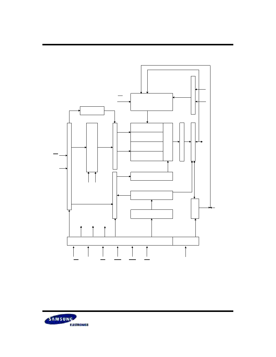
Bank Select
Timing Register DM Input Register
Addr
ess Register
Ref
r
esh C
o
unter
Row
Buf
f
er
R
o
w D
e
coder
Col. Buf
f
er
Data Input Register
Serial to parallel
4Mx32
4Mx32
4Mx32
4Mx32
Sense AMP
2-bit pref
etch
Out
put Buf
f
er
I
/
O Control
Column Decoder
Latency & Burst Length
Programming Register
S
t
robe
Gen.
CK, CK
ADD
LCKE
CK, CK
CKE
CS
RAS
CAS
WE
LCAS
LRAS LCBR LWE
LWCBR
LR
AS
LC
BR
CK, CK
32
32
16
16
LDM
X16
DQi
Data Strobe
FUNCTIONAL BLOCK DIAGRAM
DM
LDM
LWE

K4X51163PC - L(F)E/G
February 2006
Mobile-DDR SDRAM
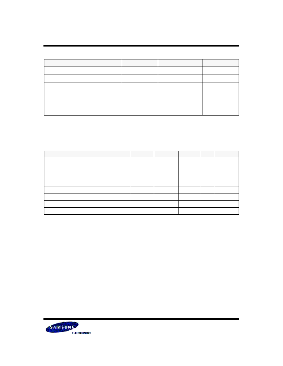
Package Dimension and Pin Configuration
Ball Name
Ball Function
CK, CK
System Differential Clock
CS
Chip Select
CKE
Clock Enable
A0 ~ A12
Address
BA0 ~ BA1
Bank Select Address
RAS
Row Address Strobe
CAS
Column Address Strobe
WE
Write Enable
L(U)DM
Data Input Mask
L(U)DQS
Data Strobe
DQ0 ~ 15
Data Input/Output
V
DD
/V
SS
Power Supply/Ground
V
DDQ
/V
SSQ
Data Output Power/Ground
< Bottom View
*1
>
60Ball(6x9) FBGA
1
2
3
7
8
9
A
V
SS
DQ15
V
SSQ
V
DDQ
DQ0
V
DD
B
V
DDQ
DQ13
DQ14
DQ1
DQ2
V
SSQ
C
V
SSQ
DQ11
DQ12
DQ3
DQ4
V
DDQ
D
V
DDQ
DQ9
DQ10
DQ5
DQ6
V
SSQ
E
V
SSQ
UDQS
DQ8
DQ7
LDQS
V
DDQ
F
V
SS
UDM
N.C.
N.C.
LDM
V
DD
G
CKE
CK
CK
WE
CAS
RAS
H
A9
A11
A12
CS
BA0
BA1
J
A6
A7
A8
A10/AP A0
A1
K
V
SS
A4
A5
A2
A3
V
DD
< Top View
*2
>
F
E
D
C
B
J
H
G
A
K
6
3
1
7
4
5
9
8
2
K4X51
163PC-
XXXX
SAMSUNG
We
e
k
#A1 Ball Origin Indicator
e
D
E
D
1
E
1
< Top View
*2
>
*2: Top View
*1: Bottom View
Symbol
Min
Typ
Max
A
-
-
1.0
A
1
0.25
-
-
E
11.4
11.5
11.6
E
1
-
6.4
-
D
9.9
10.0
10.1
D
1
-
7.2
-
e
-
0.80
-
b
0.45
0.50
0.55
z
-
-
0.10
[Unit:mm]
z
A
A1
b

K4X51163PC - L(F)E/G
February 2006
Mobile-DDR SDRAM
Input/Output Function Description
SYMBOL
TYPE
DESCRIPTION
CK, CK
Input
Clock : CK and CK are differential clock inputs. All address and control input signals are sampled on the
crossing of the positive edge of CK and negative edge of CK. Internal clock signals are derived from
CK/CK.
CKE
Input
Clock Enable : CKE HIGH activates, and CKE LOW deactivates internal clock signals, and device input
buffers and output drivers. Taking CKE LOW provides PRECHARGE POWER-DOWN and SELF
REFRESH operation (all banks idle), or ACTIVE POWER-DOWN (row ACTIVE in any bank). CKE is
synchronous for all functions except for disabling outputs, which is achieved asynchronously. Input
buffers, excluding CK, CK and CKE , are disabled during power-down and self refresh mode
which are
contrived for low standby power consumption.
CS
Input
Chip Select : CS enables(registered LOW) and disables(registered HIGH) the command decoder.
All commands are masked when CS is registered HIGH. CS provides for external bank selection on
systems with multiple banks. CS is considered part of the command code.
RAS, CAS, WE Input
Command Inputs : RAS, CAS and WE (along with CS) define the command being entered.
LDM,UDM
Input
Input Data Mask : DM is an input mask signal for write data. Input data is masked when DM is sampled
HIGH along with that input data during a WRITE access. DM is sampled on both edges of DQS. DM
pins include dummy loading internally, to matches the DQ and DQS loading. For the x16, LDM
corresponds to the data on DQ0-DQ7 ; UDM correspons to the data on DQ8-DQ15.
BA0, BA1
Input
Bank Addres Inputs : BA0 and BA1 define to which bank an ACTIVE, READ, WRITE or PRECHARGE
command is being applied.
A [n : 0]
Input
Address Inputs : Provide the row address for ACTIVE commands, and the column address and AUTO
PRECHARGE bit for READ/WRITE commands, to select one location out of the memory array in the
respective bank. A10 sampled during a PRECHARGE command
determines whether the PRECHARGE applies to one bank (A10 LOW) or all banks (A10 HIGH). If only
one bank is to be precharged, the bank is selected by BA0, BA1. The address inputs also provide the
op-code during a MODE REGISTER SET command. BA0 and BA1 determines which mode register
( mode register or extended mode register ) is loaded during the MODE REGISTER SET command.
DQ
I/O
Data Input/Output : Data bus
LDQS,UDQS
I/O
Data Strobe : Output with read data, input with write data. Edge-aligned with read data, centered in write
data. it is used to fetch write data. For the x16, LDQS corresponds to the data on DQ0-DQ7 ; UDQS
corresponds to the data on DQ8-DQ15.
NC
-
No Connect : No internal electrical connection is present.
VDDQ
Supply
DQ Power Supply : 1.7V to 1.9
5
V.
VSSQ
Supply
DQ Ground.
VDD
Supply
Power Supply : 1.7V to 1.9
5
V.
VSS
Supply
Ground.

K4X51163PC - L(F)E/G
February 2006
Mobile-DDR SDRAM
Functional Description
Figure.1 State diagram
READ
SELF
REFRESH
AUTO
REFRESH
POWER
DOWN
ROW
ACTIVE
READA
WRITEA
WRITEA
PRECHARGE
PREALL
IDLE
POWER
DOWN
REFS
REFSX
REFA
MRS
CKEL
CKEH
ACT
CKEH
CKEL
WRITE
WRITE
WRITEA
READA
PRE
PRE
READA
READA
READ
READ
Automatic Sequence
Command Sequence
WRITEA
BURST STOP
SELF
REFRESH
PARTIAL
PRE
DEEP
POWER
DOWN
CKEH
DEEP
MRS
EMRS
ALL BANKS
PRECHARGE
ON
POWER
POWER
APPLIED
POWER
DOWN
ALL BANKS
PRECHARGED
PRE

K4X51163PC - L(F)E/G
February 2006
Mobile-DDR SDRAM
Mode Register Definition
Mode Register Set(MRS)
Address Bus
A
2
A
1
A
0
Burst Length
0
0
0
Reserved
0
0
1
2
0
1
0
4
0
1
1
8
1
0
0
16
1
0
1
Reserved
1
1
0
Reserved
1
1
1
Reserved
A
3
Burst Type
0
Sequential
1
Interleave
Mode Register
BA1
BA0
A12 ~ A10/AP
A9
A8
A7
A6
A5
A4
A3
A2
A1
A0
0
BT
Burst Length
0
Figure.2 Mode Register Set
The mode register is designed to support the various operating modes of DDR SDRAM. It includes Cas latency, addressing mode,
burst length, test mode and vendor specific options to make DDR SDRAM useful for variety of applications. The default value of the
mode register is not defined, therefore the mode register must be written in the power up sequence of DDR SDRAM. The mode reg-
ister is written by asserting low on CS, RAS, CAS and WE(The DDR SDRAM should be in active mode with CKE already high prior to
writing into the mode register). The states of address pins A0 ~ A12
and BA0, BA1 in the same cycle as CS, RAS, CAS and WE
going low are written in the mode register. Two clock cycles are required to complete the write operation in the mode register. Even if
the power-up sequence is finished and some read or write operation is executed afterward, the mode register contents can be
changed with the same command and two clock cycles. This command must be issued only when all banks are in the idle state. If
mode register is changed, extended mode register automatically is reset and come into default state. So extended mode register
must be set again. The mode register is divided into various fields depending on functionality. The burst length uses A0 ~ A2,
addressing mode uses A3, Cas latency(read latency from column address) uses A4 ~ A6, A7 ~ A12 is used for test mode. BA0 and
BA1 must be set to low for proper MRS operation.
RFU*
0
0
0
CAS Latency
A6
A5
A4
CAS Latency
0
0
0
Reserved
0
0
1
Reserved
0
1
0
2
0
1
1
3
1
0
0
Reserved
1
0
1
Reserved
1
1
0
Reserved
1
1
1
Reserved
Note :
RFU(Reserved for future use) should stay "0" during MRS cycle

K4X51163PC - L(F)E/G
February 2006
Mobile-DDR SDRAM
Burst address ordering for burst length
Burst
Length
Starting
Address
(A3, A2, A1, A0)
Sequential Mode
Interleave Mode
2
xxx0
0, 1
0, 1
xxx1
1, 0
1, 0
4
xx00
0, 1, 2, 3
0, 1, 2, 3
xx01
1, 2, 3, 0
1, 0, 3, 2
xx10
2, 3, 0, 1
2, 3, 0, 1
xx11
3, 0, 1, 2
3, 2, 1, 0
8
x000
0, 1, 2, 3, 4, 5, 6, 7
0, 1, 2, 3, 4, 5, 6, 7
x001
1, 2, 3, 4, 5, 6, 7, 0
1, 0, 3, 2, 5, 4, 7, 6
x010
2, 3, 4, 5, 6, 7, 0, 1
2, 3, 0, 1, 6, 7, 4, 5
x011
3, 4, 5, 6, 7, 0, 1, 2
3, 2, 1, 0, 7, 6, 5, 4
x100
4, 5, 6, 7, 0, 1, 2, 3
4, 5, 6, 7, 0, 1, 2, 3
x101
5, 6, 7, 0, 1, 2, 3, 4
5, 4, 7, 6, 1, 0, 3, 2
x110
6, 7, 0, 1, 2, 3, 4, 5
6, 7, 4, 5, 2, 3, 0, 1
x111
7, 0, 1, 2, 3, 4, 5, 6
7, 6, 5, 4, 3, 2, 1, 0
16
0000
0, 1, 2, 3, 4, 5, 6, 7, 8, 9, 10, 11, 12, 13, 14,15
0, 1, 2, 3, 4, 5, 6, 7, 8, 9, 10, 11, 12, 13, 14,15
0001
1, 2, 3, 4, 5, 6, 7, 8, 9, 10, 11, 12, 13, 14,15, 0
1, 0, 3, 2, 5, 4, 7, 6, 9, 8, 11,10,13,12,15,14
0010
2, 3, 4, 5, 6, 7, 8, 9, 10, 11, 12, 13, 14,15, 0, 1
2, 3, 0, 1, 6, 7, 4, 5,10,11, 8, 9, 14,15,12,13
0011
3, 4, 5, 6, 7, 8, 9, 10, 11, 12, 13, 14,15, 0, 1, 2
3, 2, 1, 0, 7, 6, 5, 4,11,10, 9, 8, 15,14,13,12
0100
4, 5, 6, 7, 8, 9, 10, 11, 12, 13, 14,15, 0, 1, 2, 3
4, 5, 6, 7, 0, 1, 2, 3,12,13,14,15, 8, 9, 10,11
0101
5, 6, 7,8, 9, 10, 11, 12, 13, 14,15, 0, 1, 2, 3, 4
5, 4, 7, 6, 1, 0, 3, 2,13,12,15,14, 9, 8,11,10
0110
6, 7, 8, 9, 10, 11, 12, 13, 14,15, 0, 1, 2, 3, 4, 5
6, 7, 4, 5, 2, 3, 0, 1,14,15,12,13,10,11, 8, 9
0111
7, 8, 9, 10, 11, 12, 13, 14,15, 0, 1, 2, 3, 4, 5, 6
7, 6, 5, 4, 3, 2, 1, 0, 15,14,13,12,11,10, 9, 8
1000
8, 9, 10, 11, 12, 13, 14,15, 0, 1, 2, 3, 4, 5, 6, 7
8, 9,10,11,12,13,14,15, 0, 1, 2, 3, 4, 5, 6, 7
1001
9, 10, 11, 12, 13, 14,15, 0, 1, 2, 3, 4, 5, 6, 7, 8
9, 8, 11,10,13,12,15,14,1, 0, 3, 2, 5, 4, 7, 6
1010
10, 11, 12, 13, 14, 15, 0, 1, 2, 3, 4, 5, 6, 7, 8, 9
10,11, 8, 9, 14,15,12,13, 2, 3, 0, 1, 6, 7, 4, 5
1011
11, 12, 13, 14, 15, 0, 1, 2, 3, 4, 5, 6, 7, 8, 9, 10
11,10, 9, 8, 15,14,13,12, 3, 2, 1, 0, 7, 6, 5, 4
1100
12, 13, 14, 15, 0, 1, 2, 3, 4, 5, 6, 7, 8, 9, 10, 11
12,13,14,15, 8, 9, 10,11, 4, 5, 6, 7, 0, 1, 2, 3
1101
13, 14, 15, 0, 1, 2, 3, 4, 5, 6, 7, 8, 9, 10, 11,12
13,12,15,14, 9, 8,11,10, 5, 4, 7, 6, 1, 0, 3, 2
1110
14, 15, 0, 1, 2, 3, 4, 5, 6, 7, 8, 9, 10, 11, 12, 13
14,15,12,13,10,11, 8, 9, 6, 7, 4, 5, 2, 3, 0, 1
1111
15, 0, 1, 2, 3, 4, 5, 6, 7, 8, 9, 10, 11, 12, 13, 14
15,14,13,12,11,10, 9, 8, 7, 6, 5, 4, 3, 2, 1, 0

K4X51163PC - L(F)E/G
February 2006
Mobile-DDR SDRAM
Extended Mode Register Set(EMRS)
The extended mode register is designed to support partial array self refresh or driver strength control. EMRS cycle is not mandatory
and the EMRS command needs to be issued only when either PASR or DS is used. The default state without EMRS command
issued is half driver strength, and Full array refreshed. The extended mode register is written by asserting low on CS, RAS, CAS,
WE and high on BA1 ,low on BA0(The DDR SDRAM should be in all bank precharge with CKE already high prior to writing into the
extended mode register). The state of address pins A0 ~ A12 in the same cycle as CS, RAS, CAS and WE going low is written in the
extended mode register. Two clock cycles are required to complete the write operation in the extended mode register. Even if the
power-up sequence is finished and some read or write operations is executed afterward, the mode register contents can be changed
with the same command and two clock cycles. But this command must be issued only when all banks are in the idle state. A0 - A2
are used for partial array self refresh and A5 - A6 are used for driver strength control. "High" on BA1 and"Low" on BA0 are used for
EMRS. All the other address pins except A0,A1,A2,A5,A6, BA1, BA0 must be set to low for proper EMRS operation. Refer to the
table for specific codes.
Extended MRS for PASR(Partial Array Self Refresh) &
DS(Driver Strength Control)
Address Bus
BA1
BA0
A12 ~ A10/AP
A9
A8 A7
A6
A5
A4
A3
A2
A1
A0
Mode Register
1
PASR
0
RFU* 0 0
0
RFU*
DS
DS
A
6
A
5
Driver Strength
0
0
Full
0
1
1/2
1
0
1/4
1
1
1/8
PASR
A
2
A
1
A
0
Refreshed Area
0
0
0
Full Array
0
0
1
1/2 of Full Array
0
1
0
1/4 of Full Array
0
1
1
Reserved
1
0
0
Reserved
1
0
1
Reserved
1
1
0
Reserved
1
1
1
Reserved
Internal TCSR
Self refresh cycle is controlled
automatically by internal tem-
perature sensor and control cir-
cuit according to the three
temperature ranges ; 45
∞
C and
85
∞
C
Note :
RFU(Reserved for future use) should stay "0" during EMRS cycle
Figure.3 Extended Mode Register Set

K4X51163PC - L(F)E/G
February 2006
Mobile-DDR SDRAM
Note :
1. In order to save power consumption, Mobile-DDR SDRAM includes PASR option.
2. Mobile-DDR SDRAM supports three kinds of PASR in self refresh mode; Full array, 1/2 Array, 1/4 Array.
- Full Array
- 1/2 Array
- 1/4 Array
Partial Self Refresh Area
Figure.4 EMRS code and TCSR , PASR
Partial Array Self Refresh (PASR)
BA1=0
BA0=0
BA1=0
BA0=1
BA1=1
BA0=1
BA1=1
BA0=0
BA1=0
BA0=0
BA1=0
BA0=1
BA1=1
BA0=1
BA1=1
BA0=0
BA1=0
BA0=0
BA1=0
BA0=1
BA1=1
BA0=1
BA1=1
BA0=0
Internal Temperature Compensated Self Refresh (TCSR)
Note :
1. In order to save power consumption, Mobile DDR SDRAM includes the internal temperature sensor and control units to control the
self refresh cycle automatically according to the three temperature ranges ; 45
∞
C and 85
∞
C.
2. If the EMRS for external TCSR is issued by the controller, this EMRS code for TCSR is ignored.
3. It has +/- 5
∞
C tolerance.
Temperature Range
Self Refresh Current (IDD6)
Unit
- E
- G
Full Array
1/2 Array
1/4 Array
Full Array
1/2 Array
1/4 Array
45
∞
C
*3
300
270
255
250
220
205
uA
85
∞
C
600
500
450
500
400
350
K4X51163PC - L(F)E/G
February 2006
Mobile-DDR SDRAM
DC Operating Conditions
Absolute maximum ratings
Note :
Permanent device damage may occur if ABSOLUTE MAXIMUM RATINGS are exceeded.
Functional operation should be restricted to recommend operation condition.
Exposure to higher than recommended voltage for extended periods of time could affect device reliability.
Parameter
Symbol
Value
Unit
Voltage on any pin relative to V
SS
V
IN
, V
OUT
-0.5 ~ 2.7
V
Voltage on V
DD
supply relative to V
SS
V
DD
-0.5 ~ 2.7
V
Voltage on V
DDQ
supply relative to V
SS
V
DDQ
-0.5 ~ 2.7
V
Storage temperature
T
STG
-55 ~ +150
∞
C
Power dissipation
P
D
1.0
W
Short circuit current
I
OS
50
mA
Recommended operating conditions(Voltage referenced to VSS=0V, Tc
= -25
∞
C to 85
∞
C)
Note :
1. Under all conditions, VDDQ must be less than or equal to VDD.
2. These parameters should be tested at the pin on actual components and may be checked at either the pin or the pad in simulation.
Parameter
Symbol
Min
Max
Unit
Note
Supply voltage(for device with a nominal VDD of 1.8V)
VDD
1.7
1.95
V
1
I/O Supply voltage
VDDQ
1.7
1.95
V
1
Input logic high voltage
VIH(DC)
0.7 x VDDQ
VDDQ+0.3
V
2
Input logic low voltage
VIL(DC)
-0.3
0.3 x VDDQ
V
2
Output logic high voltage
VOH(DC)
0.9 x VDDQ
-
V
IOH = -0.1mA
Output logic low voltage
VOL(DC)
-
0.1 x VDDQ
V
IOL = 0.1mA
Input leakage current
II
-2
2
uA
Output leakage current
IOZ
-5
5
uA
K4X51163PC - L(F)E/G
February 2006
Mobile-DDR SDRAM
DC CHARACTERISTICS
Recommended operating conditions (Voltage referenced to V
SS
= 0V, Tc = -25 to 85
∞
C)
Parameter
Symbol
Test Condition
DDR266
DDR222
Unit
Operating Current
(One Bank Active)
IDD0
tRC = tRCmin ; tCK = tCKmin ; CKE is HIGH; CS is HIGH between valid commands;
address inputs are SWITCHING; data bus inputs are STABLE
80
70
mA
Precharge Standby Current in
power-down mode
IDD2P
all banks idle, CKE is LOW; CS is HIGH, tCK = t CKmin ; address and control inputs are
SWITCHING; data bus inputs are STABLE
0.3
mA
IDD2PS
all banks idle, CKE is LOW; CS is HIGH, CK = LOW, CK = HIGH;
address and control
inputs are SWITCHING; data bus inputs are STABLE
0.3
Precharge Standby Current
in non power-down mode
IDD2N
all banks idle, CKE is HIGH; CS is HIGH, tCK = t CKmin ;address and control inputs are
SWITCHING; data bus inputs are STABLE
12
10
mA
IDD2NS all banks idle, CKE is HIGH; CS is HIGH, CK = LOW, CK = HIGH; address and control
inputs are SWITCHING; data bus inputs are STABLE
8
7
Active Standby Current
in power-down mode
IDD3P
one bank active, CKE is LOW; CS is HIGH, tCK = tCKmin ;address and control inputs are
SWITCHING; data bus inputs are STABLE
6
mA
IDD3PS
one bank active, CKE is LOW; CS is HIGH, CK = LOW, CK = HIGH;address and control
inputs are SWITCHING; data bus inputs are STABLE
3
Active Standby Current
in non power-down mode
(One Bank Active)
IDD3N
one bank active, CKE is HIGH; CS is HIGH, tCK = tCKmin ;address and control inputs
are SWITCHING; data bus inputs are STABLE
25
20
mA
IDD3NS
one bank active, CKE is HIGH; CS is HIGH, CK = LOW, CK = HIGH;
address and control inputs are SWITCHING; data bus inputs are STABLE
20
15
Operating Current
(Burst Mode)
IDD4R
one bank active; BL = 4; CL = 3; tCK = tCKmin ; continuous read bursts; I OUT = 0 mA
address inputs are SWITCHING; 50% data change each burst transfer
115
95
mA
IDD4W
one bank active; BL = 4; tCK = tCKmin ; continuous write bursts;address inputs are
SWITCHING; 50% data change each burst transfer
100
90
Refresh Current
IDD5
tRC = tRFCmin ; tCK = tCKmin ; burst refresh; CKE is HIGH;address and control inputs
are SWITCHING; data bus inputs are STABLE
150
135
mA
Self Refresh Current
IDD6
CKE is LOW; tCK = tCKmin ;
Extended Mode Register set to all 0's;
address and control inputs are STABLE; data bus inputs
are STABLE
TCSR
45*
1
85
∞
C
-E
Full Array
300
600
uA
1/2 Array
270
500
1/4 Array
255
450
-G
Full Array
250
500
1/2 Array
220
400
1/4 Array
205
350
Deep Power Down Current
IDD8*
2
Address and control inputs are STABLE; data bus inputs are STABLE
10
uA
Note :
1. It has +/- 5
∞
C
tolerance.
2. DPD(Deep Power Down) function is an optional feature, and it will be enabled upon request.
Please contact Samsung for more information.
3. IDD specifications are tested after the device is properly intialized.
4. Input slew rate is 1V/ns.
5. Definitions for IDD: LOW is defined as V
IN
0.1 * VDDQ ;
HIGH is defined as V
IN
0.9 * VDDQ ;
STABLE is defined as inputs stable at a HIGH or LOW level ;
SWITCHING is defined as: - address and command: inputs changing between HIGH and LOW once per two clock cycles ;
- data bus inputs: DQ changing between HIGH and LOW once per clock cycle; DM and DQS are STABLE.
K4X51163PC - L(F)E/G
February 2006
Mobile-DDR SDRAM
AC Operating Conditions & Timming Specification
Note :
1. These parameters should be tested at the pin on actual components and may be checked at either the pin or the pad in simulation.
2. The value of V
IX
is expected to equal 0.5*V
DDQ
of the transmitting device and must track variations in the DC level of the same.
Parameter/Condition
Symbol
Min
Max
Unit
Note
Input High (Logic 1) Voltage, all inputs
VIH(AC)
0.8 x VDDQ
VDDQ+0.3
V
1
Input Low (Logic 0) Voltage, all inputs
VIL(AC)
-0.3
0.2 x VDDQ
V
1
Input Crossing Point Voltage, CK and CK inputs
VIX(AC)
0.4 x VDDQ
0.6 x VDDQ
V
2
K4X51163PC - L(F)E/G
February 2006
Mobile-DDR SDRAM
AC Timming Parameters & Specifications
Parameter
Symbol
DDR266
DDR222
Unit
Note
Min
Max
Min
Max
Clock cycle time
CL=2
tCK
12.0
15.0
ns
CL=3
7.5
9.0
Row cycle time
tRC
67.5
81
ns
Row active time
tRAS
45
70,000
54
70,000
ns
RAS to CAS delay
tRCD
22.5
27
ns
Row precharge time
tRP
22.5
27
ns
Row active to Row active delay
tRRD
15
15
ns
Write recovery time
tWR
15
15
ns
Last data in to Active delay
tDAL
2tCK+tRP
2tCK+tRP
-
2
Last data in to Read command
tCDLR
1
1
tCK
Col. address to Col. address delay
tCCD
1
1
tCK
Clock high level width
tCH
0.45
0.55
0.45
0.55
tCK
Clock low level width
tCL
0.45
0.55
0.45
0.55
tCK
DQ Output data access time from CK/
CK
CL=2
tAC
2
8
2.5
8
ns
3
CL=3
2
6
2.5
6
DQS Output data access time from
CK/CK
CL=2
tDQSCK
2
8
2.5
8
ns
CL=3
2
6
2.5
6
Data strobe edge to ouput data edge
tDQSQ
0.6
0.7
ns
Read Preamble
CL=2
tRPRE
0.5
1.1
0.5
1.1
tCK
CL=3
0.9
1.1
0.9
1.1
Read Postamble
tRPST
0.4
0.6
0.4
0.6
tCK
CK to valid DQS-in
tDQSS
0.75
1.25
0.75
1.25
tCK
DQS-in setup time
tWPRES
0
0
ns
4
DQS-in hold time
tWPREH
0.25
0.25
tCK
DQS-in high level width
tDQSH
0.4
0.6
0.4
0.6
tCK
DQS-in low level width
tDQSL
0.4
0.6
0.4
0.6
tCK
DQS falling edge to CK setup time
tDSS
0.2
0.2
tCK
DQS falling edge hold time from CK
tDSH
0.2
0.2
tCK
DQS-in cycle time
tDSC
0.9
1.1
0.9
1.1
tCK
Address and Control Input setup time
tIS
1.3
1.5
ns
1
Address and Control Input hold time
tIH
1.3
1.5
ns
1
Address & Control input pulse width
tIPW
2.6
3.0
1
DQ & DM setup time to DQS
tDS
0.8
1.1
ns
5,6
DQ & DM hold time to DQS
tDH
0.8
1.1
ns
5,6
DQ & DM input pulse width
tDIPW
1.8
2.4
ns
DQ & DQS low-impedence time from CK/CK
tLZ
1.0
1.0
ns
DQ & DQS high-impedence time from CK/CK
tHZ
6.0
7.0
ns
DQS write postamble time
tWPST
0.4
0.6
0.4
0.6
tCK
DQS write preamble time
tWPRE
0.25
0.25
tCK
K4X51163PC - L(F)E/G
February 2006
Mobile-DDR SDRAM
Parameter
Symbol
DDR266
DDR222
Unit
Note
Min
Max
Min
Max
Refresh interval time
tREF
64
64
ms
Mode register set cycle time
tMRD
2
2
tCK
Power down exit time
tPDEX
1*tCK +tIS
1*tCK +tIS
ns
CKE min. pulse width(high and low pulse width)
tCKE
2
2
tCK
Auto refresh cycle time
tRFC
80
90
ns
7
Exit self refresh to active command
tXSR
120
120
ns
Data hold from DQS to earliest DQ edge
tQH
tHPmin -
tQHS
tHPmin -
tQHS
ns
Data hold skew factor
tQHS
0.75
1.0
ns
Clock half period
tHP
tCLmin or
tCHmin
tCLmin or
tCHmin
ns
K4X51163PC - L(F)E/G
February 2006
Mobile-DDR SDRAM
Note :
1. Input Setup/Hold Slew Rate Derating
This derating table is used to increase t
IS
/t
IH
in the case where the input slew rate is below 1.0V/ns.
2. Minimum 3CLK of tDAL(= tWR + tRP) is required because it need minimum 2CLK for tWR and minimum 1CLK for tRP.
3. tAC(min) value is measured at the high Vdd(1.95V) and cold temperature(-25
∞
C).
tAC(max) value is measured at the low Vdd(1.7V) and hot temperature(85
∞
C).
tAC is measured in the device with half driver strength and under the AC output load condition (Fig.7 in next Page).
4. The specific requirement is that DQS be valid(High or Low) on or before this CK edge. The case shown(DQS going from
High_Z to logic Low) applies when no writes were previously in progress on the bus. If a previous write was in progress,
DQS could be High at this time, depending on tDQSS.
5. I/O Setup/Hold Slew Rate Derating
This derating table is used to increase t
DS
/t
DH
in the case where the I/O slew rate is below 1.0V/ns.
6. I/O Delta Rise/Fall Rate(1/slew-rate) Derating
This derating table is used to increase tDS/tDH in the case where the DQ and DQS slew rates differ. The Delta Rise/Fall Rate
is calculated as 1/SlewRate1-1/SlewRate2. For example, if slew rate 1 = 1.0V/ns and slew rate 2 =0.8V/ns, then the Delta Rise/Fall
Rate =-0.25ns/V.
7. Maximum burst refresh cycle : 8
Input Setup/Hold Slew Rate
tIS
tIH
(V/ns)
(ps)
(ps)
1.0
0
0
0.8
+50
+50
0.6
+100
+100
I/O Setup/Hold Slew Rate
tDS
tDH
(V/ns)
(ps)
(ps)
1.0
0
0
0.8
+75
+75
0.6
+150
+150
Delta Rise/Fall Rate
tDS
tDH
(ns/V)
(ps)
(ps)
0
0
0
±
0.25
+50
+50
±
0.5
+100
+100
K4X51163PC - L(F)E/G
February 2006
Mobile-DDR SDRAM
AC Operating Test Conditions
(V
DD
= 1.7V to 1.95V, T
c
= -25 to 85
∞
C)
Parameter
Value
Unit
AC input levels (Vih/Vil)
0.8 x VDDQ / 0.2 x VDDQ
V
Input timing measurement reference level
0.5 x VDDQ
V
Input signal minimum slew rate
1.0
V/ns
Output timing measurement reference level
0.5 x VDDQ
V
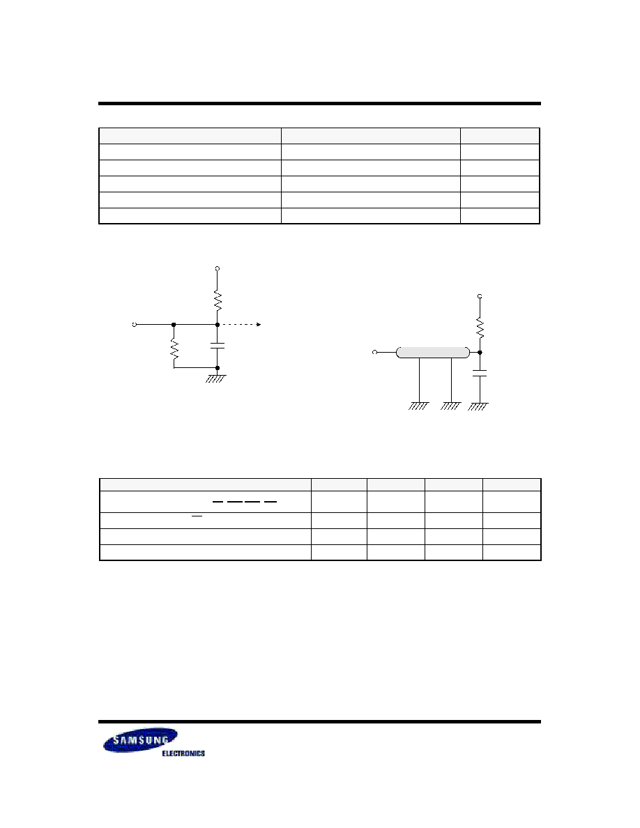
Output load condition
See Figure.7
1.8V
13.9K
10.6K
Output
20pF
V
OH
(DC) = 0.9 x VDDQ , I
OH
= -0.1mA
V
OL
(DC) = 0.1 x VDDQ , I
OL
= 0.1mA
Vtt=0.5 x V
DDQ
50
Output
20pF
Z0=50
Input/Output Capacitance
(V
DD
=1.8
,
V
DDQ
=1.8V
,
T
C
= 25
∞
C
,
f=1MHz)
Parameter
Symbol
Min
Max
Unit
Input capacitance
(A0 ~ A12, BA0 ~ BA1, CKE, CS, RAS,CAS, WE)
CIN1
1.5
3.0
pF
Input capacitance( CK, CK )
CIN2
1.5
3.5
pF
Data & DQS input/output capacitance
COUT
2.0
4.5
pF
Input capacitance(DM)
CIN3
2.0
4.5
pF
Figure.6 DC Output Load Circuit
Figure.7 AC Output Load Circuit

K4X51163PC - L(F)E/G
February 2006
Mobile-DDR SDRAM
AC Overshoot/Undershoot Specification for Address & Control Pins
Parameter
Specification
Maximum peak Amplitude allowed for overshoot area
0.9V
Maximum peak Amplitude allowed for undershoot area
0.9V
Maximum overshoot area above VDD
3V-ns
Maximum undershoot area below VSS
3V-ns
Overshoot Area
Maximum Amplitude
V
DD
Undershoot Area
Maximum Amplitude
V
SS
Volts
(V)
Figure.8 AC Overshoot and Undershoot Definition for Address and Control Pins
Time (ns)
AC Overshoot/Undershoot Specification for CLK, DQ, DQS and DM Pins
Parameter
Specification
Maximum peak Amplitude allowed for overshoot area
0.9V
Maximum peak Amplitude allowed for undershoot area
0.9V
Maximum overshoot area above VDDQ
3V-ns
Maximum undershoot area below VSSQ
3V-ns
Overshoot Area
Maximum Amplitude
V
DDQ
Undershoot Area
Maximum Amplitude
V
SSQ
Volts
(V)
Figure.9 AC Overshoot and Undershoot Definition for CLK, DQ, DQS and DM Pins
Time (ns)

K4X51163PC - L(F)E/G
February 2006
Mobile-DDR SDRAM
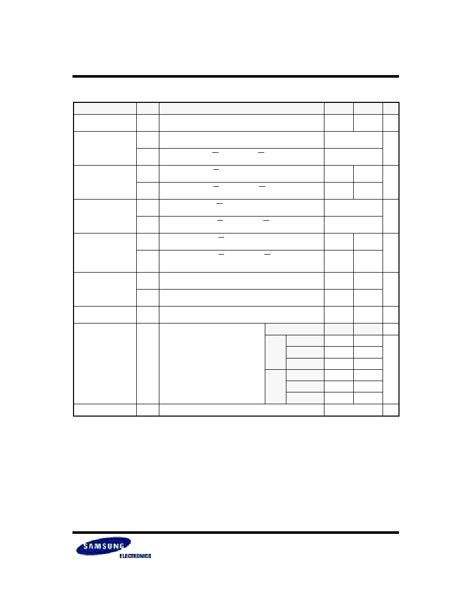
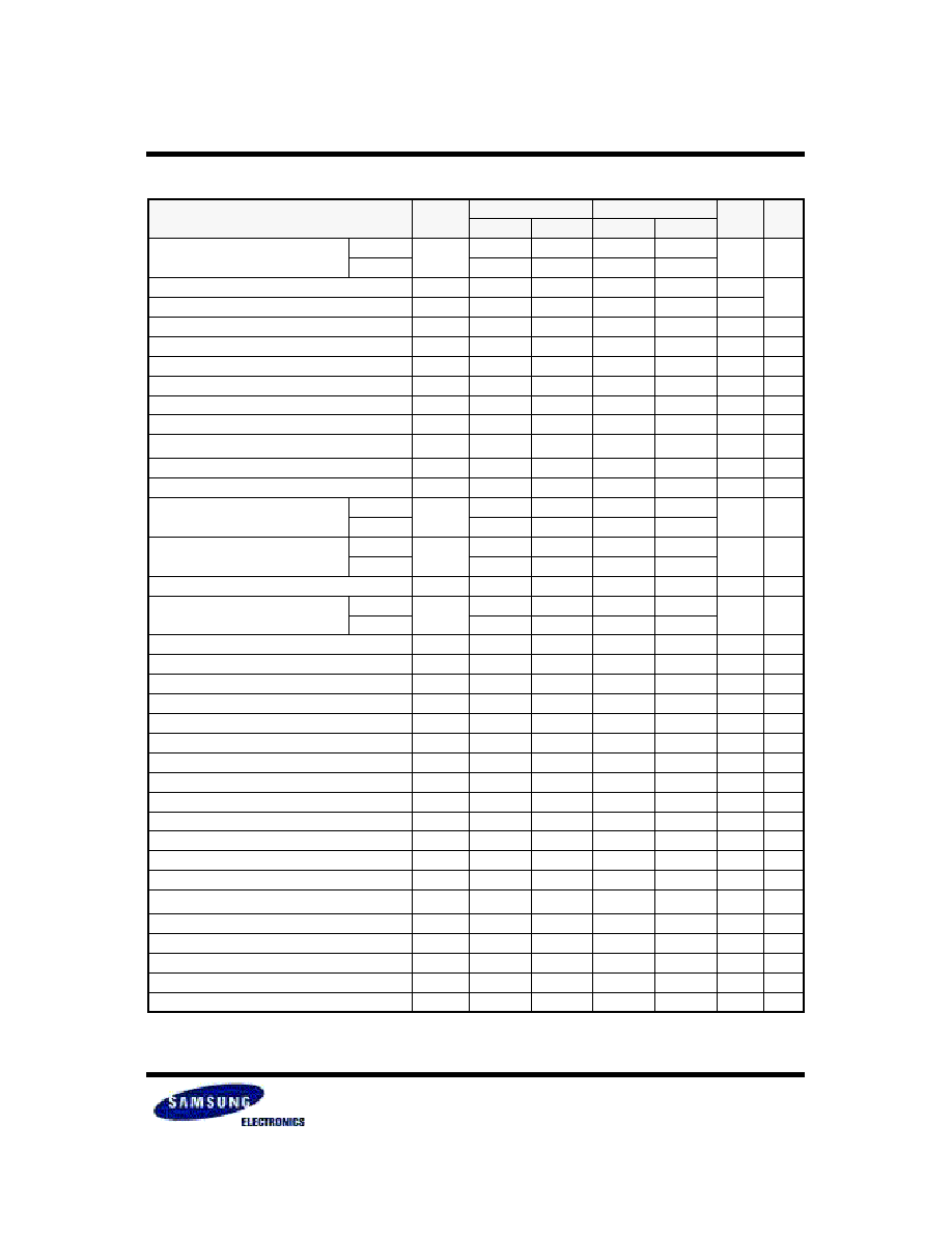
Command Truth Table
(V=Valid, X=Don
t Care, H=Logic High, L=Logic Low)
COMMAND
CKEn-1 CKEn
CS
RAS
CAS
WE
BA0,1 A10/AP
A12,A11,
A9 ~ A0
Note
Register
Mode Register Set
H
X
L
L
L
L
OP CODE
1, 2
Refresh
Auto Refresh
H
H
L
L
L
H
X
3
Self
Refresh
Entry
L
3
Exit
L
H
L
H
H
H
X
3
H
X
X
X
3
Bank Active & Row Addr.
H
X
L
L
H
H
V
Row Address
Read &
Column Address
Auto Precharge Disable
H
X
L
H
L
H
V
L
Column
Address
(A0~A9)
4
Auto Precharge Enable
H
4
Write &
Column Address
Auto Precharge Disable
H
X
L
H
L
L
V
L
Column
Address
(A0~A9)
4
Auto Precharge Enable
H
4, 6
Deep Power Down
Entry
H
L
L
H
H
L
X
Exit
L
H
H
X
X
X
Burst Stop
H
X
L
H
H
L
X
7
Precharge
Bank Selection
H
X
L
L
H
L
V
L
X
All Banks
X
H
5
Active Power Down
Entry
H
L
H
X
X
X
X
L
V
V
V
Exit
L
H
X
X
X
X
Precharge Power Down
Entry
H
L
H
X
X
X
X
L
H
H
H
Exit
L
H
H
X
X
X
L
V
V
V
DM
H
X
X
8
No operation (NOP) : Not defined
H
X
H
X
X
X
X
9
L
H
H
H
9
Note :
1. OP Code : Operand Code. A0 ~ A12 & BA0 ~ BA1 : Program keys. (@EMRS/MRS)
2.EMRS/ MRS can be issued only at all banks precharge state.
A new command can be issued 2 clock cycles after EMRS or MRS.
3. Auto refresh functions are same as the CBR refresh of DRAM.
The automatical precharge without row precharge command is meant by "Auto".
Auto/self refresh can be issued only at all banks precharge state.
4. BA0 ~ BA1 : Bank select addresses.
5. If A10/AP is "High" at row precharge, BA0 and BA1 are ignored and all banks are selected.
6. During burst write with auto precharge, new read/write command can not be issued.
Another bank read/write command can be issued after the end of burst.
New row active of the associated bank can be issued at tRP after the end of burst.
7. Burst stop command is valid at every burst length.
8. DM sampled at the rising and falling edges of the DQS and Data-in are masked at the both edges (Write DM latency is 0).
9. This combination is not defined for any function, which means "No Operation(NOP)" in DDR SDRAM.

K4X51163PC - L(F)E/G
February 2006
Mobile-DDR SDRAM
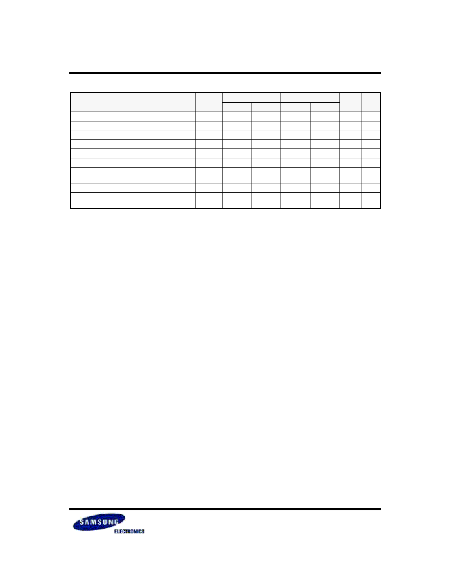
Functional Truth Table
Current State
CS
RAS
CAS
WE
Address
Command
Action
PRECHARGE
STANDBY
L
H
H
L
X
Burst Stop
ILLEGAL
*2
L
H
L
X
BA, CA, A10
READ/WRITE
ILLEGAL
*2
L
L
H
H
BA, RA
Active
Bank Active, Latch RA
L
L
H
L
BA, A10
PRE/PREA
ILLEGAL
*4
L
L
L
H
X
Refresh
AUTO-Refresh
*5
L
L
L
L
Op-Code, Mode-Add
MRS
Mode Register Set
*5
ACTIVE
STANDBY
L
H
H
L
X
Burst Stop
NOP
L
H
L
H
BA, CA, A10
READ/READA
Begin Read, Latch CA,
Determine Auto-Precharge
L
H
L
L
BA, CA, A10
WRITE/WRITEA
Begin Write, Latch CA,
Determine Auto-Precharge
L
L
H
H
BA, RA
Active
Bank Active/ILLEGAL
*2
L
L
H
L
BA, A10
PRE/PREA
Precharge/Precharge All
L
L
L
H
X
Refresh
ILLEGAL
L
L
L
L
Op-Code, Mode-Add
MRS
ILLEGAL
READ
L
H
H
L
X
Burst Stop
Terminate Burst
L
H
L
H
BA, CA, A10
READ/READA
Terminate Burst, Latch CA,
Begin New Read, Determine
Auto-Precharge
*3
L
H
L
L
BA, CA, A10
WRITE/WRITEA
ILLEGAL
L
L
H
H
BA, RA
Active
Bank Active/ILLEGAL
*2
L
L
H
L
BA, A10
PRE/PREA
Terminate Burst, Precharge
L
L
L
H
X
Refresh
ILLEGAL
L
L
L
L
Op-Code, Mode-Add MRS
ILLEGAL

K4X51163PC - L(F)E/G
February 2006
Mobile-DDR SDRAM
Functional truth table
Current State
CS
RAS
CAS
WE
Address
Command
Action
WRITE
L
H
H
L
X
Burst Stop
ILLEGAL
L
H
L
H
BA, CA, A10
READ/READA
Terminate Burst With DM=High, Latch CA,
Begin Read, Determine Auto-Precharge
*3
L
H
L
L
BA, CA, A10
WRITE/WRITEA
Terminate Burst, Latch CA,
Begin new Write, Determine Auto-Pre-
charge
*3
L
L
H
H
BA, RA
Active
Bank Active/ILLEGAL
*2
L
L
H
L
BA, A10
PRE/PREA
Terminate Burst With DM=High,
Precharge
L
L
L
H
X
Refresh
ILLEGAL
L
L
L
L
Op-Code, Mode-Add MRS
ILLEGAL
READ with
AUTO
PRECHARGE
*6
(READA)
L
H
H
L
X
Burst Stop
ILLEGAL
L
H
L
H
BA, CA, A10
READ/READA
*6
L
H
L
L
BA, CA, A10
WRITE/WRITEA ILLEGAL
L
L
H
H
BA, RA
Active
*6
L
L
H
L
BA, A10
PRE/PREA
*6
L
L
L
H
X
Refresh
ILLEGAL
L
L
L
L
Op-Code, Mode-Add MRS
ILLEGAL
WRITE with
AUTO
RECHARGE
*7
(WRITEA)
L
H
H
L
X
Burst Stop
ILLEGAL
L
H
L
H
BA, CA, A10
READ/READA
*7
L
H
L
L
BA, CA, A10
WRITE/WRITEA *7
L
L
H
H
BA, RA
Active
*7
L
L
H
L
BA, A10
PRE/PREA
*7
L
L
L
H
X
Refresh
ILLEGAL
L
L
L
L
Op-Code, Mode-Add MRS
ILLEGAL
K4X51163PC - L(F)E/G
February 2006
Mobile-DDR SDRAM
Functional truth table
Current State
CS
RAS
CAS
WE
Address
Command
Action
PRECHARGING
(DURING tRP)
L
H
H
L
X
Burst Stop
ILLEGAL
*2
L
H
L
X
BA, CA, A10
READ/WRITE
ILLEGAL
*2
L
L
H
H
BA, RA
Active
ILLEGAL
*2
L
L
H
L
BA, A10
PRE/PREA
NOP
*4
(Idle after tRP)
L
L
L
H
X
Refresh
ILLEGAL
L
L
L
L
Op-Code, Mode-Add
MRS
ILLEGAL
ROW
ACTIVATING
(FROM ROW
ACTIVE TO
tRCD)
L
H
H
L
X
Burst Stop
ILLEGAL
*2
L
H
L
X
BA, CA, A10
READ/WRITE
ILLEGAL
*2
L
L
H
H
BA, RA
Active
ILLEGAL
*2
L
L
H
L
BA, A10
PRE/PREA
ILLEGAL
*2
L
L
L
H
X
Refresh
ILLEGAL
L
L
L
L
Op-Code, Mode-Add
MRS
ILLEGAL
WRITE
RECOVERING
(DURING tWR
OR tCDLR)
L
H
H
L
X
Burst Stop
ILLEGAL
*2
L
H
L
H
BA, CA, A10
READ
ILLEGAL
*2
L
H
L
L
BA, CA, A10
WRITE
WRITE
L
L
H
H
BA, RA
Active
ILLEGAL
*2
L
L
H
L
BA, A10
PRE/PREA
ILLEGAL
*2
L
L
L
H
X
Refresh
ILLEGAL
L
L
L
L
Op-Code, Mode-Add
MRS
ILLEGAL

K4X51163PC - L(F)E/G
February 2006
Mobile-DDR SDRAM
Functional truth table
Current State
CS
RAS
CAS
WE
Address
Command
Action
RE-
FRESHING
L
H
H
L
X
Burst Stop
ILLEGAL
L
H
L
X
BA, CA, A10
READ/WRITE
ILLEGAL
L
L
H
H
BA, RA
Active
ILLEGAL
L
L
H
L
BA, A10
PRE/PREA
ILLEGAL
L
L
L
H
X
Refresh
ILLEGAL
L
L
L
L
Op-Code, Mode-Add
MRS
ILLEGAL
MODE
REGISTER
SETTING
L
H
H
L
X
Burst Stop
ILLEGAL
L
H
L
X
BA, CA, A10
READ/WRITE
ILLEGAL
L
L
H
H
BA, RA
Active
ILLEGAL
L
L
H
L
BA, A10
PRE/PREA
ILLEGAL
L
L
L
H
X
Refresh
ILLEGAL
L
L
L
L
Op-Code, Mode-Add
MRS
ILLEGAL

K4X51163PC - L(F)E/G
February 2006
Mobile-DDR SDRAM
Functional truth table
ABBREVIATIONS :
H=High Level, L=Low level, X=Don
t Care
Note :
1. All entries assume that CKE was High during the preceding clock cycle and the current clock cycle.
2. ILLEGAL to bank in specified state ; function may be legal in the bank indicated by BA, depending on the state of that bank.(ILLEGAL = Device oper-
ation and/or data integrity are not guaranteed.)
3. Must satisfy bus contention, bus turn around and write recovery requirements.
4. NOP to bank precharging or in idle sate. May precharge bank indicated by BA.
5. ILLEGAL if any bank is not idle.
6. Refer to "Read with Auto Precharge Timing Diagram" for detailed information.
7. Refer to "Write with Auto Precharge Timing Diagram" for detailed information.
8. CKE Low to High transition will re-enable CK, CK and other inputs asynchronously. A minimum setup time must be satisfied before issuing any com-
mand other than EXIT.
9. Power-Down, Self-Refresh and Deep Power Down Mode can be entered only from All Bank Idle state.
10. The Deep Power Down Mode is exited by asserting CKE high and full initialization is required after exiting Deep Power Down Mode.
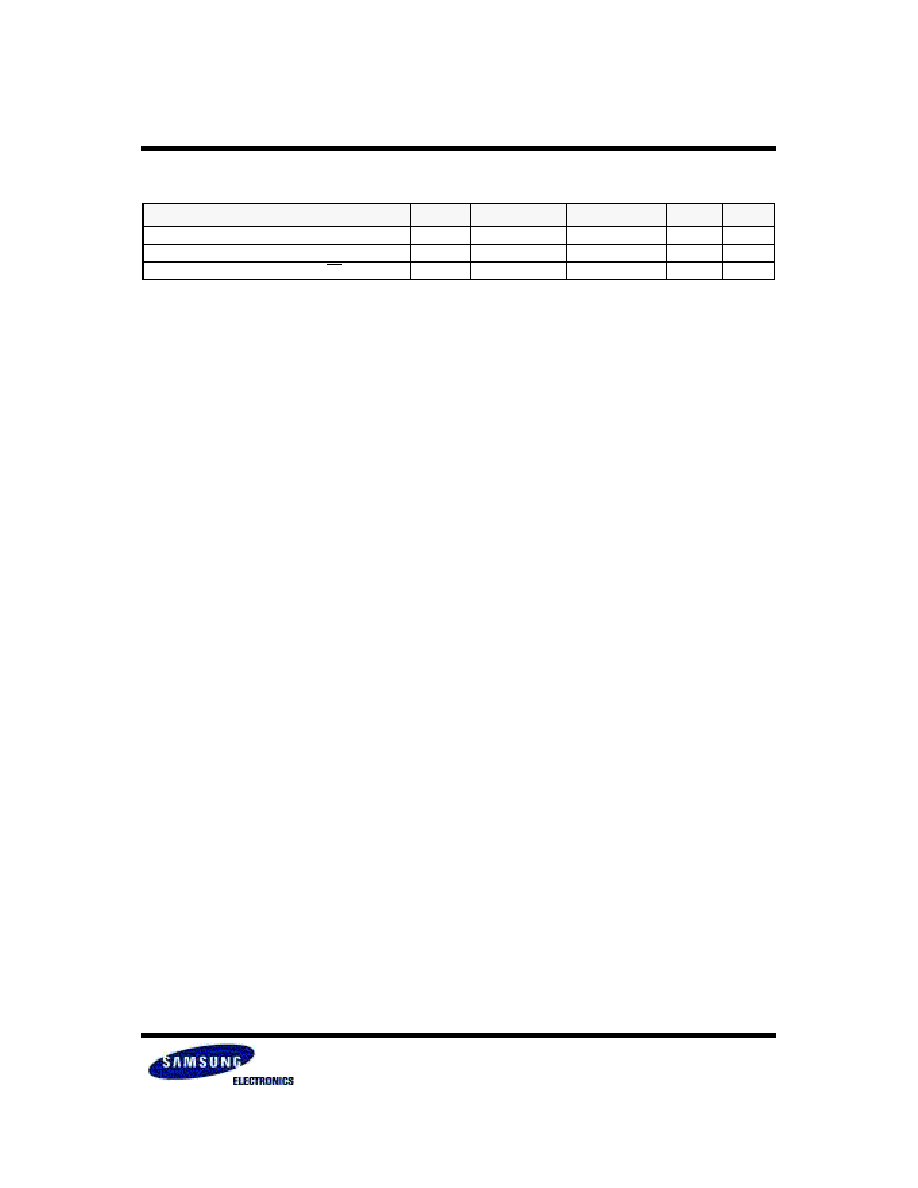
Current State
CKE
n-1
CKE
n
CS
RAS
CAS
WE
Add
Action
SELF-
REFRESHING
*8
L
H
H
X
X
X
X
Exit Self-Refresh
L
H
L
H
H
H
X
Exit Self-Refresh
L
H
L
H
H
L
X
ILLEGAL
L
H
L
H
L
X
X
ILLEGAL
L
H
L
L
X
X
X
ILLEGAL
L
L
X
X
X
X
X
NOPeration(Maintain Self-Refresh)
POWER
DOWN
L
H
X
X
X
X
X
Exit Power Down(Idle after tPDEX)
L
L
X
X
X
X
X
NOPeration(Maintain Power Down)
DEEP POWER
DOWN
L
H
H
X
X
X
X
Exit Deep Power Down
*10
L
L
X
X
X
X
X
NOPeration(Maintain Deep Power Down)
ALL BANKS
IDLE*9
H
H
X
X
X
X
X
Refer to Function True Table
H
L
L
L
L
H
X
Enter Self-Refresh
H
L
H
X
X
X
X
Enter Power Down
H
L
L
H
H
H
X
Enter Power Down
H
L
L
H
H
L
X
Enter Deep Power Down
H
L
L
H
H
L
X
ILLEGAL
H
L
L
H
L
X
X
ILLEGAL
H
L
L
L
X
X
X
ILLEGAL
L
X
X
X
X
X
X
Refer to Current State=Power Down
ANY STATE
other than
listed above
H
H
X
X
X
X
X
Refer to Function Truth Table