
K5D5657DCM-F015
Revision 0.0
June 2003
- 1 -
MCP MEMORY
Preliminary
256Mb NAND and 256Mb Mobile SDRAM
MCP Specification of

K5D5657DCM-F015
Revision 0.0
June 2003
- 2 -
MCP MEMORY
Preliminary
Document Title
Multi-Chip Package MEMORY
256M Bit(32Mx8) Nand Flash / 256M Bit(4Mx16x4Banks) Mobile SDRAM
Revision History
The attached datasheets are prepared and approved by SAMSUNG Electronics. SAMSUNG Electronics CO., LTD. reserve the right
to change the specifications. SAMSUNG Electronics will evaluate and reply to your requests and questions about device. If you have
any questions, please contact the SAMSUNG branch office near you.
Revision No.
0.0
Remark
Preliminary
History
Initial issue.
(256Mb NAND C-Die_Ver 1.0)
(256Mb MSDRAM E`-Die_Ver 0.5)
Draft Date
June 23, 2003
Note : For more detailed features and specifications including FAQ, please refer to Samsung's web site.
http://samsungelectronics.com/semiconductors/products/products_index.html

K5D5657DCM-F015
Revision 0.0
June 2003
- 3 -
MCP MEMORY
Preliminary
GENERAL DESCRIPTION
FEATURES
<Common>
∑
Operating Temperature : -25
∞
C ~ 85
∞
C
∑
Package : 107-ball FBGA Type - 10.5x13mm, 0.8mm pitch
<NAND>
∑
Power Supply Voltage :
2.4~2.9V
∑
Organization
- Memory Cell Array : (32M + 1024K)bit x 8bit
- Data Register : (512 + 16)bit x 8bit
∑
Automatic Program and Erase
- Page Program : (512 + 16)Byte
- Block Erase : (16K + 512)Byte
∑
Page Read Operation
- Page Size : (512 + 16)Byte
- Random Access : 10
µ
s(Max.)
- Serial Page Access : 50ns(Min.)
∑
Fast Write Cycle Time
- Program time : 200
µ
s(Typ.)
- Block Erase Time : 2ms(Typ.)
∑
Command/Address/Data Multiplexed I/O Port
∑
Hardware Data Protection
- Program/Erase Lockout During Power Transitions
∑
Reliable CMOS Floating-Gate Technology
- Endurance : 100K Program/Erase Cycles
- Data Retention : 10 Years
∑
Command Register Operation
∑
Intelligent Copy-Back
∑
Unique ID for Copyright Protection
<Mobile SDRAM>
∑
Power Supply Voltage : 1.65~1.95V
∑ LVCMOS compatible with multiplexed address.
∑ Four banks operation.
∑ MRS cycle with address key programs.
-. CAS latency (1, 2 & 3).
-. Burst length (1, 2, 4, 8 & Full page).
-. Burst type (Sequential & Interleave).
∑ EMRS cycle with address key programs.
∑ All inputs are sampled at the positive going edge of the system
clock.
∑ Burst read single-bit write operation.
∑ Special Function Support.
-. PASR (Partial Array Self Refresh).
-. Internal TCSR (Temperature Compensated Self Refresh)
-. DS (Driver Strength)
∑ DQM for masking.
∑ Auto refresh.
∑ 64ms refresh period (4K cycle).
∑ Commercial Temperature Operation (-25
∞
C ~ 70
∞
C).
Multi-Chip Package MEMORY
256M Bit (32Mx8) Nand Flash / 256M Bit
(4Mx16x4Banks) Mobile SDRAM
The K5D5657DCM is a Multi Chip Package Memory which combines 256Mbit Nand Flash Memory and 256Mbit synchronous high
data rate Dynamic RAM.
256Mbit NAND Flash memory is organized as 32M x8 bits and 256Mbit SDRAM is organized as 4M x16 bits x4 banks.
In 256Mbit NAND Flash, a 528-Byte page program can be typically achieved within 200us and an 16K-Byte block erase can be typi-
cally achieved within 2ms. In serial read operation, a byte can be read by 50ns. DQ pins serve as the ports for address and data
input/output as well as command inputs. Even the write-intensive systems can take advantage of FLASH
s extended reliability of
100K program/erase cycles with real time mapping-out algorithm. These algorithms have been implemented in many mass storage
applications.
In 256Mbit SDRAM, Synchronous design make a device controlled precisely with the use of system clock and I/O transactions are
possible on every clock cycle. Range of operating frequencies, programmable burst length and programmable latencies allow the
same device to be useful for a variety of high bandwidth, high performance memory system applications.
The K5D5657DCM is suitable for use in data memory of mobile communication system to reduce not only mount area but also power
consumption. This device is available in 107-ball FBGA Type.
K5D5657DCM-F015
Revision 0.0
June 2003
- 4 -
MCP MEMORY
Preliminary
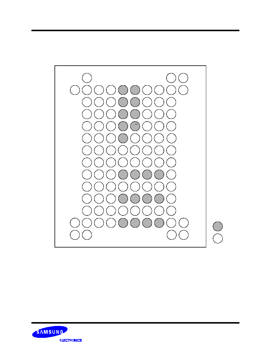
PIN CONFIGURATION
107 FBGA: Top View (Ball Down)
1
2
3
4
5
6
7
8
NC
DQ0d
Vdd
Vss
Vcc
NC
A3
NC
Vss
DQ2d
DQ1d
CLE
/CE
A0
A1
A2
Vddq
DQ4d
DQ3d
ALE
/WE
BA0
BA1
A10
Vssq
DQ6d
DQ5d
/RE
R/B
/RAS
NC
/CS
Vddq
NC
DQ7d
/WP
NC
/CAS
Vss
LDQM
NC
A12
CKE
Vdd
Vdd
UDQM
CLK
A8
A9
A11
Vssq
NC
DQ8d
IO0
IO2
IO4
IO6
A7
Vddq
DQ9d
DQ10d
NC
NC
NC
NC
A6
Vssq
DQ11d
DQ12d
IO1
IO3
IO5
IO7
A5
Vdd
DQ13d
DQ14d
NC
NC
NC
NC
A4
NC
DQ15d
Vss
Vss
Vccq
Vcc
Vss
NC
A
B
C
D
E
F
G
H
J
K
L
M
Vss
/WEd
DNU
DNU
DNU
DNU
DNU
DNU
DNU
DNU
DNU
DNU
DNU
N
P
NAND
MSDRAM
NC
NC
NC
NC
9 10
K5D5657DCM-F015
Revision 0.0
June 2003
- 5 -
MCP MEMORY
Preliminary
NOTE :
1. Samsung are not designed or manufactured for use in a device or system that is used under circumstance in which human life is potentially at stake.
Please contact to the memory marketing team in samsung electronics when considering the use of a product contained herein for any specific purpose,
such as medical, aerospace, nuclear, military, vehicular or undersea repeater use.
PIN DESCRIPTION
Pin Name
Pin Function(Mobile SDRAM)
CLK
System Clock
CKE
Clock Enable
/CS
Chip Select
/RAS
Row Address Strobe
/CAS
Column Address Strobe
/WEd
Write Enable
A0 ~ A12
Address Input
BA0 ~ BA1
Bank Address Input
LDQM
Lower Input/Output Data Mask
UDQM
Upper Input/Output Data Mask
DQ0d ~ DQ15d
Data Input/Output
Vdd
Power Supply
Vddq
Data Out Power
Vss
Ground
Vssq
DQ Ground
Pin Name
Pin Function(NAND Flash)
/CE
Chip Enable
/RE
Read Enable
/WP
Write Protection
/WE
Write Enable
ALE
Address Latch Enable
CLE
Command Latch Enable
R/B
Ready/Busy Output
IO0 ~ IO7
Data Input/Output
Vcc
Power Supply
Vccq
Data Out Power
Vss
Ground
Pin Name
Pin Function
NC
No Connection
DNU
Do Not Use
ORDERING INFORMATION
K 5 D 56 57 D C M - F 0 15
Samsung
MCP Memory(2chips)
Device Type
NAND Flash + Mobile SDRAM
NAND Flash Density,
Organization
56 : 256Mbit, x8
Flash Block Architecture
C = Uniform Block
Version
M= 1st Generation
Mobile SDRAM Speed
15 = 15ns, CL=2
Operating Voltage
D: 2.6V / 1.8V
Package
F = FBGA(Leaded)
Mobile SDRAM Density, Organization
57 : 256Mbit, x16
NAND Flash Speed
0 = None

K5D5657DCM-F015
Revision 0.0
June 2003
- 6 -
MCP MEMORY
Preliminary
FUNCTIONAL BLOCK DIAGRAM
CLE
CE
WP
ALE
Vccq
X-Buffers
256M+8M Bit
Command
NAND flash
ARRAY
(512 + 16)Byte x 65536
Y-Gating
page Register & S/A
I/O Buffers & Latches
Latches
& Decoders
Y-Buffers
Latches
& Decoders
Register
Control Logic
& High Voltage
Generator
Global Buffers
Output
R/B
RE
WE
IO0 to IO7
Vss
Vcc
Bank Select
Data Input Register
4M x 16
4M x 16
S
e
n
s
e
A
M
P
O
u
t
p
u
t
B
u
f
f
e
r
I
/
O
C
o
n
t
r
o
l
Column Decoder
Latency & Burst Length
Programming Register
A
d
d
r
e
s
s
R
e
g
i
s
t
e
r
R
o
w
B
u
f
f
e
r
R
e
f
r
e
s
h
C
o
u
n
t
e
r
R
o
w
D
e
c
o
d
e
r
C
o
l
.
B
u
f
f
e
r
L
R
A
S
L
C
B
R
4M x 16
4M x 16
T
i
m
i
n
g
R
e
g
i
s
t
e
r
CS
CAS
Vss
RAS
CKE
Vddq
WEd
CLK
A0~A12
LDQM
BA0~BA1
UDQM
Vdd
DQ0d to DQ15d
Vssq
Driver

K5D5657DCM-F015
Revision 0.0
June 2003
- 7 -
MCP MEMORY
Preliminary
256Mb(32M x 8)
NAND Flash C-Die

K5D5657DCM-F015
Revision 0.0
June 2003
- 8 -
MCP MEMORY
Preliminary
512Byte
16 Byte
Figure 1. NAND Flash(x8) ARRAY ORGANIZATION
NOTE: 1. Column Address : Starting Address of the Register.
2. 00h Command(Read) : Defines the starting address of the 1st half of the register.
3. 01h Command(Read) : Defines the starting address of the 2nd half of the register.
4. A8 is set to "Low" or "High" by the 00h or 01h Command.
5. The device ignores any additional input of address cycles than reguired.
I/O 0
I/O 1
I/O 2
I/O 3
I/O 4
I/O 5
I/O 6
I/O 7
1st Cycle
A
0
A
1
A
2
A
3
A
4
A
5
A
6
A
7
2nd Cycle
A
9
A
10
A
11
A
12
A
13
A
14
A
15
A
16
3rd Cycle
A
17
A
18
A
19
A
20
A
21
A
22
A
23
A
24
1st half Page Register
(=256 Bytes)
2nd half Page Register
(=256 Bytes)
64K Pages
(=2,048 Blocks)
512 Byte
8 bit
16 Byte
1 Block =32 Pages
= (16K + 512) Byte
I/O 0 ~ I/O 7
1 Page = 528 Byte
1 Block = 528 Byte x 32 Pages
= (16K + 512) Byte
1 Device = 528Bytes x 32Pages x 2048 Blocks
= 264 Mbits
Column Address
Row Address
(Page Address)
Page Register

K5D5657DCM-F015
Revision 0.0
June 2003
- 9 -
MCP MEMORY
Preliminary
PRODUCT INTRODUCTION
This device is a 264Mbit(276,824,064 bit) memory organized as 65,536 rows(pages) by 528 columns. Spare eight columns are
located from column address of 512~527. A 528-byte data register is connected to memory cell arrays accommodating data transfer
between the I/O buffers and memory during page read and page program operations. The memory array is made up of 16 cells that
are serially connected to form a NAND structure. Each of the 16 cells resides in a different page. A block consists of the 32 pages
formed by two NAND structures, totaling 8448 NAND structures of 16 cells. The array organization is shown in Figure1. The program
and read operations are executed on a page basis, while the erase operation is executed on a block basis. The memory array con-
sists of 2048 separately erasable 16K-Byte blocks. It indicates that the bit by bit erase operation is prohibited on this device.
This device has addresses multiplexed into 8 I/O`s. This device allows sixteen bit wide data transport into and out of page registers.
This scheme dramatically reduces pin counts while providing high performance and allows systems upgrades to future densities by
maintaining consistency in system board design. Command, address and data are all written through I/O
s by bringing WE to low
while CE is low. Data is latched on the rising edge of WE. Command Latch Enable(CLE) and Address Latch Enable(ALE) are used to
multiplex command and address respectively, via the I/O pins. Some commands require one bus cycle. For example, Reset com-
mand, Read command, Status Read command, etc require just one cycle bus. Some other commands like Page Program and Copy-
back Program and Block Erase, require two cycles: one cycle for setup and the other cycle for execution. The 32M-byte physical
space requires 24 addresses, thereby requiring three cycles for word-level addressing: column address, low row address and high
row address, in that order. Page Read and Page Program need the same three address cycles following the required command input.
In Block Erase operation, however, only the two row address cycles are used. Device operations are selected by writing specific com-
mands into the command register. Table 1 defines the specific commands of this device.
The device includes one block sized OTP(One Time Programmable), which can be used to increase system security or to provide
identification capabilities. Detailed information can be obtained by contact with Samsung.
Table 1. COMMAND SETS
Caution : Any undefined command inputs are prohibited except for above command set of Table 1.
Function
1st. Cycle
2nd. Cycle
Acceptable Command during Busy
Read 1
00h/01h
-
Read 2
50h
-
Read ID
90h
-
Reset
FFh
-
O
Page Program
80h
10h
Copy-Back Program
00h
8Ah
Read Block Lock Status
7Ah
Block Erase
60h
D0h
Read Status
70h
-
O

K5D5657DCM-F015
Revision 0.0
June 2003
- 10 -
MCP MEMORY
Preliminary
DC AND OPERATING CHARACTERISTICS
(Recommended operating conditions otherwise noted.)
Parameter
Symbol
Test Conditions
Min
Typ
Max
Unit
Operating
Current
Sequential Read
I
CC
1
tRC=50ns, CE=V
IL
I
OUT
=0mA
-
10
20
mA
Program
I
CC
2
-
-
10
25
Erase
I
CC
3
-
-
10
25
Stand-by Current(TTL)
I
SB
1
CE=V
IH
, WP=0V/V
CC
-
-
1
Stand-by Current(CMOS)
I
SB
2
CE=V
CC
-0.2, WP=0V/V
CC
-
10
50
µ
A
Input Leakage Current
I
LI
V
IN
=0 to Vcc(max)
-
-
±
10
Output Leakage Current
I
LO
V
OUT
=0 to Vcc(max)
-
-
±
10
Input High Voltage
V
IH
I/O pins
V
CCQ
-0.4
-
V
CCQ
+0.3
V
Except I/O pins
V
CC
-0.4
-
V
CC
+0.3
Input Low Voltage, All inputs
V
IL
-
-0.3
-
0.5
Output High Voltage Level
V
OH
I
OH
=-100
µ
A
V
CC
Q-0.4
-
-
Output Low Voltage Level
V
OL
I
OL
=100uA
-
-
0.4
Output Low Current(R/B)
I
OL
(R/B)
V
OL
=0.1V
3
4
-
mA
RECOMMENDED OPERATING CONDITIONS
Parameter
Symbo
Min
Typ.
Max
Unit
Supply Voltage
V
CC
2.4
2.65
2.9
V
Supply Voltage
V
CCQ
2.4
2.65
2.9
V
Supply Voltage
V
SS
0
0
0
V
ABSOLUTE MAXIMUM RATINGS
NOTE :
1. Minimum DC voltage is -0.6V on input/output pins. During transitions, this level may undershoot to -2.0V for periods <30ns.
Maximum DC voltage on input/output pins is V
CC,
+0.3V which, during transitions, may overshoot to V
CC
+2.0V for periods <20ns.
2. Permanent device damage may occur if ABSOLUTE MAXIMUM RATINGS are exceeded. Functional operation should be restricted to the conditions
as detailed in the operational sections of this data sheet. Exposure to absolute maximum rating conditions for extended periods may affect reliability.
Parameter
Symbol
Rating
Unit
Voltage on any pin relative to V
SS
V
IN/OUT
-0.6 to + 4.6
V
V
CC
-0.6 to + 4.6
V
CCQ
-0.6 to + 4.6
Temperature Under Bias
T
BIAS
-40 to +125
∞
C
Storage Temperature
T
STG
-65 to +150
∞
C
Short Circuit Current
Ios
5
mA
K5D5657DCM-F015
Revision 0.0
June 2003
- 11 -
MCP MEMORY
Preliminary
CAPACITANCE
(T
A
=25
∞
C, VCC=2.65V , f=1.0MHz)
NOTE : Capacitance is periodically sampled and not 100% tested.
Item
Symbol
Test Condition
Min
Max
Unit
Input/Output Capacitance
C
I/O
V
IL
=0V
-
10
pF
Input Capacitance
C
IN
V
IN
=0V
-
10
pF
VALID BLOCK
NOTE :
1. This device may include invalid blocks when first shipped. Additional invalid blocks may develop while being used. The number of valid blocks is pre-
sented with both cases of invalid blocks considered. Invalid blocks are defined as blocks that contain one or more bad bits
.
Do not erase or program
factory-marked bad blocks. Refer to the attached technical notes for a appropriate management of invalid blocks.
2. The 1st block, which is placed on 00h block address, is fully guaranteed to be a valid block, does not require Error Correction.
3. The 2nd and 3rd blocks are good upon shipping.
Parameter
Symbol
Min
Typ.
Max
Unit
Valid Block Number
N
VB
2013
-
2048
Blocks
AC TEST CONDITION
( Vcc=2.4V~2.9V , T
A
=-40 to 85
∞
C)
Parameter
Value
Input Pulse Levels
0V to VccQ
Input Rise and Fall Times
5ns
Input and Output Timing Levels
VccQ/2
Output Load (VccQ:2.65V +/-10%)
1 TTL GATE and CL=30pF
MODE SELECTION
NOTE : 1. X can be V
IL
or V
IH.
2. WP should be biased to CMOS high or CMOS low for standby.
CLE
ALE
CE
WE
RE
PRE
WP
Mode
H
L
L
H
X
X
Read Mode
Command Input
L
H
L
H
X
X
Address Input(3clock)
H
L
L
H
X
H
Write Mode
Command Input
L
H
L
H
X
H
Address Input(3clock)
L
L
L
H
X
H
Data Input
L
L
L
H
X
X
Data Output
X
X
X
X
X
X
H
During Program(Busy)
X
X
X
X
X
X
H
During Erase(Busy)
X
X
(1)
X
X
X
X
L
Write Protect
X
X
H
X
X
0V/V
CC
(2)
0V/V
CC
(2)
Stand-by
Program/Erase Characteristics
Parameter
Symbol
Min
Typ
Max
Unit
Program Time
t
PROG
-
200
500
µ
s
Dummy Busy Time for the Lock or Lock-tight Block
t
LBSY
-
5
10
µ
s
Number of Partial Program Cycles
in the Same Page
Main Array
Nop
-
-
2
cycles
Spare Array
-
-
3
cycles
Block Erase Time
t
BERS
-
2
3
ms
K5D5657DCM-F015
Revision 0.0
June 2003
- 12 -
MCP MEMORY
Preliminary
AC Timing Characteristics for Command / Address / Data Input
NOTE
:
1. If t
CS
is set less than 10ns, t
WP
must be minimum 35ns, otherwise, t
WP
may be minimum 25ns.
Parameter
Symbol
Min
Max
Unit
CLE Set-up Time
t
CLS
0
-
ns
CLE Hold Time
t
CLH
10
-
ns
CE Setup Time
t
CS
0
.-
ns
CE Hold Time
t
CH
10
-
ns
WE Pulse Width
t
WP
25
(1)
-
ns
ALE Setup Time
t
ALS
0
-
ns
ALE Hold Time
t
ALH
10
-
ns
Data Setup Time
t
DS
20
-
ns
Data Hold Time
t
DH
10
-
ns
Write Cycle Time
t
WC
45
-
ns
WE High Hold Time
t
WH
15
-
ns
AC Characteristics for Operation
NOTE :
1. If reset command(FFh) is written at Ready state, the device goes into Busy for maximum 5us.
2. To break the sequential read cycle, CE must be held high for longer time than tCEH.
3. The time to Ready depends on the value of the pull-up resistor tied R/B pin.
Parameter
Symbol
Min
Max
Unit
Data Transfer from Cell to Register
t
R
-
10
µ
s
ALE to RE Delay
t
AR
10
-
ns
CLE to RE Delay
t
CLR
10
-
ns
Ready to RE Low
t
RR
20
-
ns
RE Pulse Width
t
RP
25
-
ns
WE High to Busy
t
WB
-
100
ns
Read Cycle Time
t
RC
50
-
ns
CE Access Time
t
CEA
-
45
ns
RE Access Time
t
REA
-
30
ns
RE High to Output Hi-Z
t
RHZ
-
30
ns
CE High to Output Hi-Z
t
CHZ
-
20
ns
RE or CE High to Output hold
t
OH
15
-
ns
RE High Hold Time
t
REH
15
-
ns
Output Hi-Z to RE Low
t
IR
0
-
ns
WE High to RE Low
t
WHR1
60
-
ns
WE High to RE Low in Block Lcok Mode
t
WHR2
100
-
ns
Device Resetting Time
(Read/Program/Erase)
t
RST
-
5/10/500
(1)
µ
s
K5D5657DCM-F015
Revision 0.0
June 2003
- 13 -
MCP MEMORY
Preliminary
NAND Flash Technical Notes
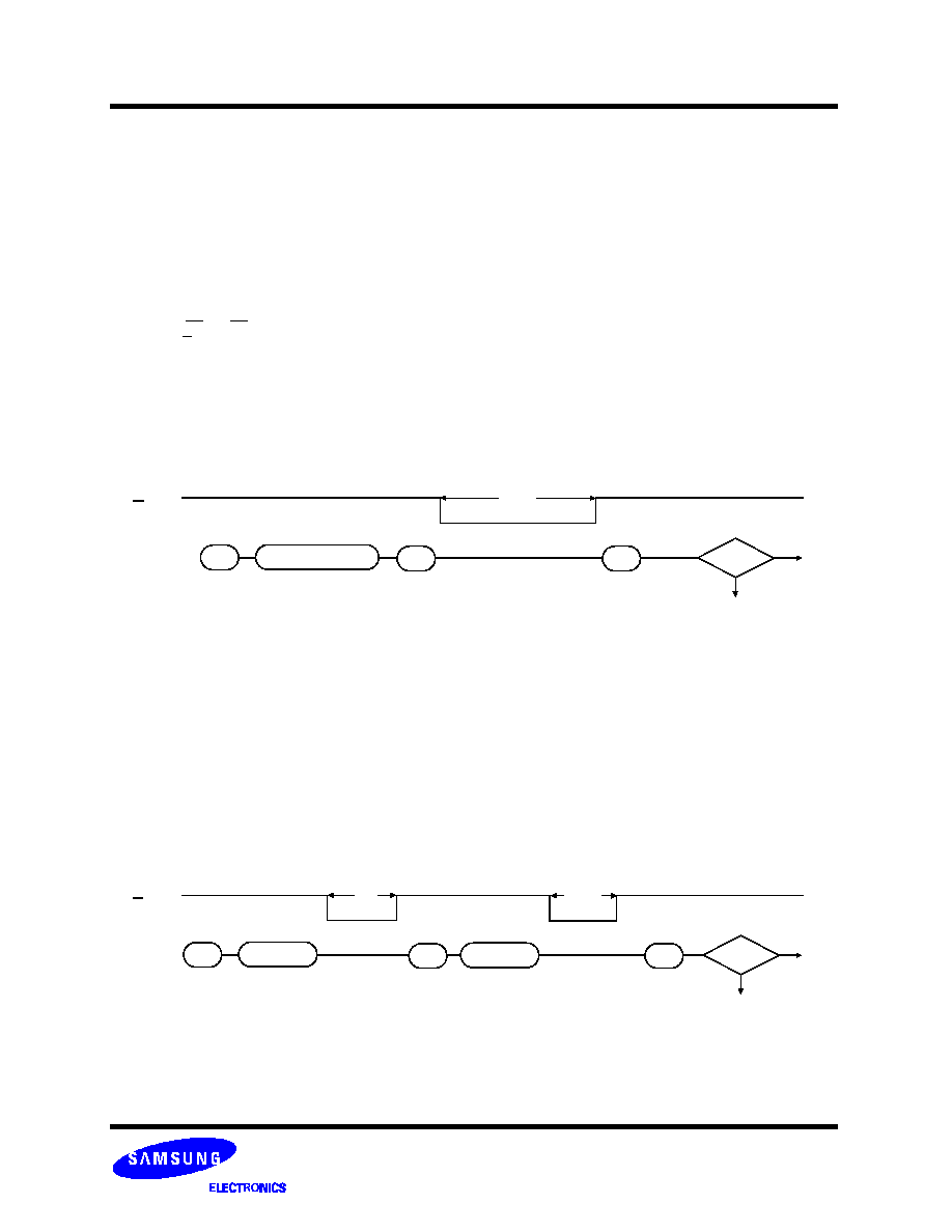
Identifying Invalid Block(s)
Invalid Block(s)
Invalid blocks are defined as blocks that contain one or more invalid bits whose reliability is not guaranteed by Samsung. The infor-
mation regarding the invalid block(s) is so called as the invalid block information. Devices with invalid block(s) have the same quality
level as devices with all valid blocks and have the same AC and DC characteristics. An invalid block(s) does not affect the perfor-
mance of valid block(s) because it is isolated from the bit line and the common source line by a select transistor. The system design
must be able to mask out the invalid block(s) via address mapping. The 1st block, which is placed on 00h block address, is fully guar-
anteed to be a valid block, does not require Error Correction.
All device locations are erased(FFh) except locations where the invalid block(s) information is written prior to shipping. The invalid
block(s) status is defined by the 6th byte in the spare area. Samsung makes sure that either the 1st or 2nd page of every invalid block
has non-FFh data at the column address of 517. Since the invalid block information is also erasable in most cases, it is impossible to
recover the information once it has been erased. Therefore, the system must be able to recognize the invalid block(s) based on the
original invalid block information and create the invalid block table via the following suggested flow chart(Figure 2). Any intentional
erasure of the original invalid block information is prohibited.
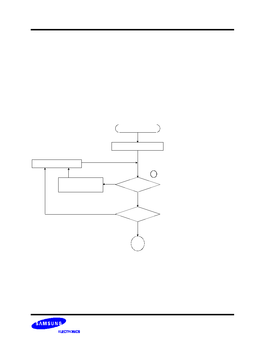
*
Check "FFh" at the column address 517
Figure 2. Flow chart to create invalid block table.
Start
Set Block Address = 0
Check "FFh" ?
Increment Block Address
Last Block ?
End
No
Yes
Yes
Create (or update)
No
Invalid Block(s) Table
of the 1st and 2nd page in the block
K5D5657DCM-F015
Revision 0.0
June 2003
- 14 -
MCP MEMORY
Preliminary
NAND Flash Technical Notes
(Continued)
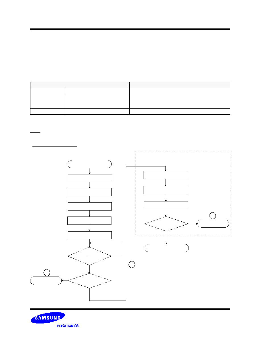
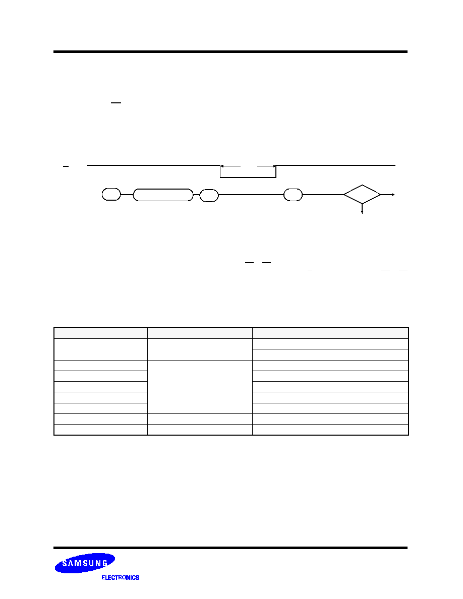
Program Flow Chart
Start
I/O 6 = 1 ?
Write 00h
I/O 0 = 0 ?
No
*
If ECC is used, this verification
Write 80h
Write Address
Write Data
Write 10h
Read Status Register
Write Address
Wait for tR Time
Verify Data
No
Program Completed
or R/B = 1 ?
Program Error
Yes
No
Yes
*
Program Error
Yes
: If program operation results in an error, map out
the block including the page in error and copy the
target data to another block.
*
operation is not needed.
Error in write or read operation
Within its life time, the additional invalid blocks may develop with NAND Flash memory. Refer to the qualification report for the actual
data.The following possible failure modes should be considered to implement a highly reliable system. In the case of status read fail-
ure after erase or program, block replacement should be done. Because program status fail during a page program does not affect
the data of the other pages in the same block, block replacement can be executed with a page-sized buffer by finding an erased
empty block and reprogramming the current target data and copying the rest of the replaced block. To improve the efficiency of mem-
ory space, it is recommended that the read or verification failure due to single bit error be reclaimed by ECC without any block
replacement. The said additional block failure rate does not include those reclaimed blocks.
Failure Mode
Detection and Countermeasure sequence
Write
Erase Failure
Status Read after Erase --> Block Replacement
Program Failure
Status Read after Program --> Block Replacement
Read back ( Verify after Program) --> Block Replacement
or ECC Correction
Read
Single Bit Failure
Verify ECC -> ECC Correction
ECC
: Error Correcting Code --> Hamming Code etc.
Example) 1bit correction & 2bit detection
K5D5657DCM-F015
Revision 0.0
June 2003
- 15 -
MCP MEMORY
Preliminary
Erase Flow Chart
Start
I/O 6 = 1 ?
I/O 0 = 0 ?
No
*
Write 60h
Write Block Address
Write D0h
Read Status Register
or R/B = 1 ?
Erase Error
Yes
No
: If erase operation results in an error, map out
the failing block and replace it with another block.
*
Erase Completed
Yes
Read Flow Chart
Start
Verify ECC
No
Write 00h
Write Address
Read Data
ECC Generation
Reclaim the Error
Page Read Completed
Yes
NAND Flash Technical Notes
(Continued)
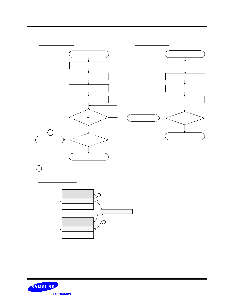
Block Replacement
* Step1
When an error happens in the nth page of the Block 'A' during erase or program operation.
* Step2
Copy the nth page data of the Block 'A' in the buffer memory to the nth page of another free block. (Block 'B')
* Step3
Then, copy the data in the 1st ~ (n-1)th page to the same location of the Block 'B'.
* Step4
Do not further erase Block 'A' by creating an 'invalid Block' table or other appropriate scheme.
Buffer memory of the controller.
1st
Block A
Block B
(n-1)th
nth
(page)
1
2
{
1st
(n-1)th
nth
(page)
{
an error occurs.

K5D5657DCM-F015
Revision 0.0
June 2003
- 16 -
MCP MEMORY
Preliminary
Samsung NAND Flash has three address pointer commands as a substitute for the two most significant column addresses. '00h'
command sets the pointer to 'A' area(0~255byte), '01h' command sets the pointer to 'B' area(256~511byte), and '50h' command sets
the pointer to 'C' area(512~527byte). With these commands, the starting column address can be set to any of a whole
page(0~527byte). '00h' or '50h' is sustained until another address pointer command is inputted. '01h' command, however, is effective
only for one operation. After any operation of Read, Program, Erase, Reset, Power_Up is executed once with '01h' command, the
address pointer returns to 'A' area by itself. To program data starting from 'A' or 'C' area, '00h' or '50h' command must be inputted
before '80h' command is written. A complete read operation prior to '80h' command is not necessary. To program data starting from
'B' area, '01h' command must be inputted right before '80h' command is written.
00h
(1) Command input sequence for programming 'A' area
Address / Data input
80h
10h
00h
80h
10h
Address / Data input
The address pointer is set to 'A' area(0~255), and sustained
01h
(2) Command input sequence for programming 'B' area
Address / Data input
80h
10h
01h
80h
10h
Address / Data input
'B', 'C' area can be programmed.
It depends on how many data are inputted.
'01h' command must be rewritten before
every program operation
The address pointer is set to 'B' area(256~512), and will be reset to
'A' area after every program operation is executed.
50h
(3) Command input sequence for programming 'C' area
Address / Data input
80h
10h
50h
80h
10h
Address / Data input
Only 'C' area can be programmed.
'50h' command can be omitted.
The address pointer is set to 'C' area(512~527), and sustained
'00h' command can be omitted.
It depends on how many data are inputted.
'A','B','C' area can be programmed.
Pointer Operation
Table 2. Destination of the pointer
Command
Pointer position
Area
00h
01h
50h
0 ~ 255 byte
256 ~ 511 byte
512 ~ 527 byte
1st half array(A)
2nd half array(B)
spare array(C)
"A" area
256 Byte
(00h plane)
"B" area
(01h plane)
"C" area
(50h plane)
256 Byte
16 Byte
"A"
"B"
"C"
Internal
Page Register
Pointer select
commnad
(00h, 01h, 50h)
Pointer
Figure 3. Block Diagram of Pointer Operation

K5D5657DCM-F015
Revision 0.0
June 2003
- 17 -
MCP MEMORY
Preliminary
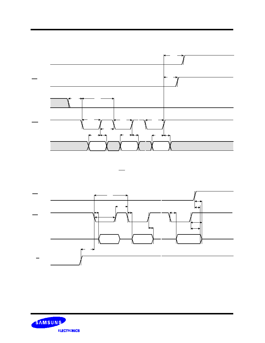
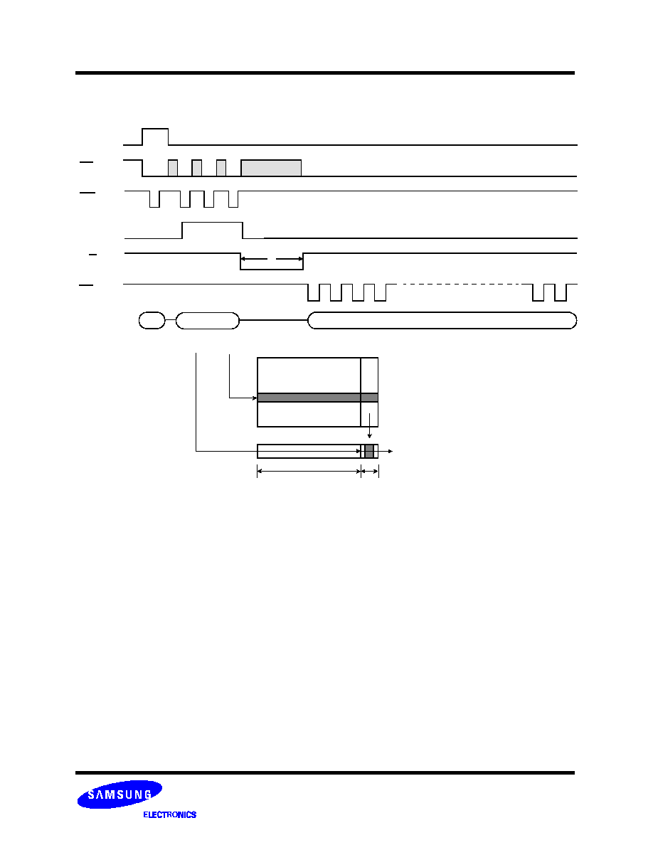
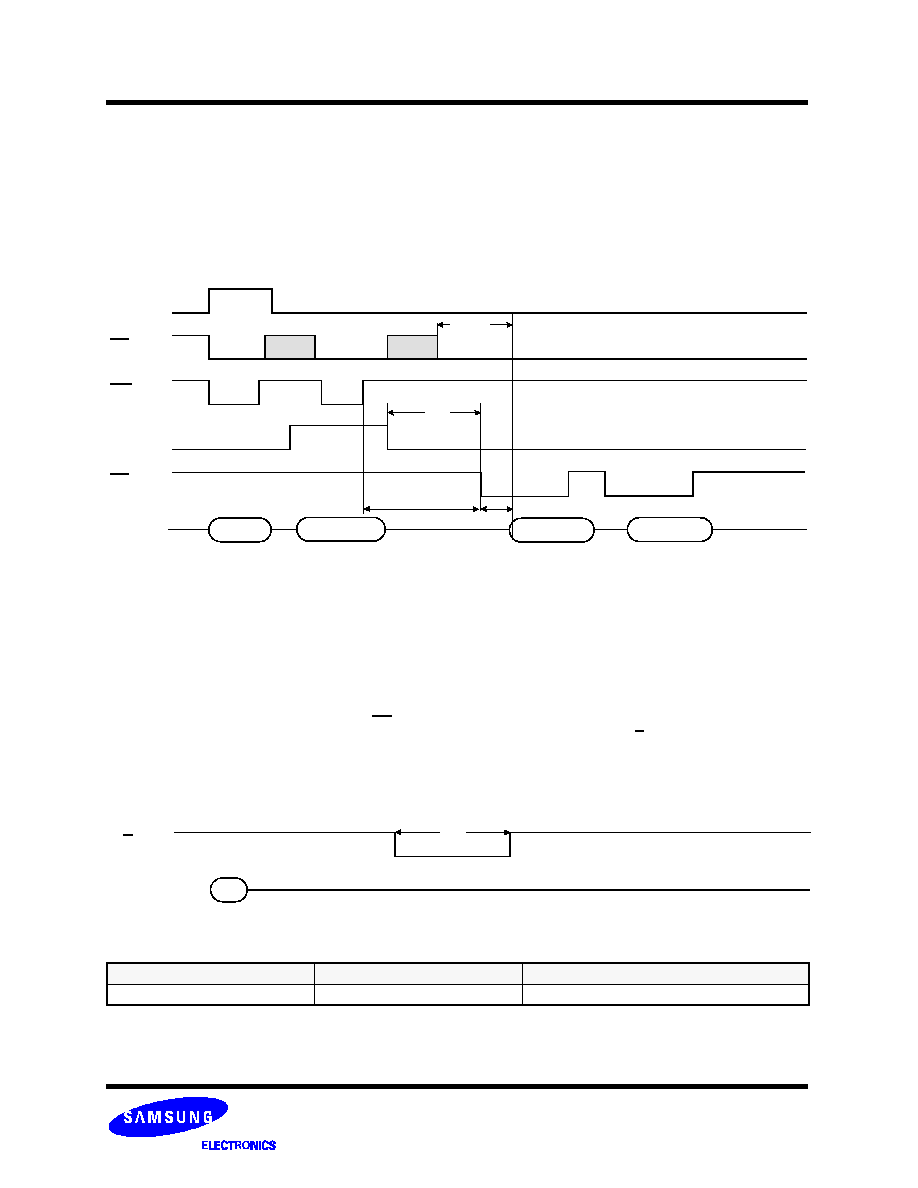
System Interface Using CE don't-care.
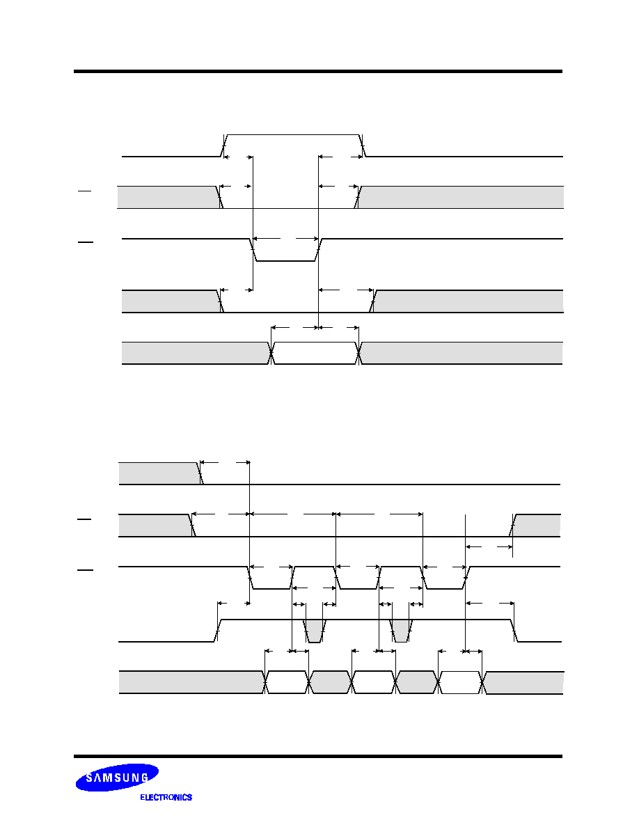
For an easier system interface, CE may be inactive during the data-loading or sequential data-reading as shown below. The internal
528byte page registers are utilized as seperate buffers for this operation and the system design gets more flexible. In addition, for
voice or audio applications which use slow cycle time on the order of u-seconds, de-activating CE during the data-loading and reading
would provide significant savings in power consumption.
Start Add.(3Cycle)
00h
CE
CLE
ALE
WE
Data Output(sequential)
CE don't-care
R/B
t
R
RE
Figure 4. Program Operation with CE don't-care.
Figure 5. Read Operation with CE don't-care.
I/Ox
CE
WE
t
WP
t
CH
t
CS
Start Add.(3Cycle)
80h
Data Input
CE
CLE
ALE
WE
Data Input
CE don't-care
10h
t
CEA
out
t
REA
CE
RE
I/Ox
I/Ox
t
OH
K5D5657DCM-F015
Revision 0.0
June 2003
- 18 -
MCP MEMORY
Preliminary
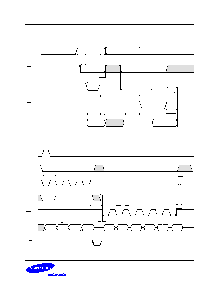
Command Latch Cycle
CE
WE
CLE
ALE
I/Ox
Command
t
CLS
t
CS
t
CLH
t
CH
t
WP
t
ALS
t
ALH
t
DS
t
DH
CE
WE
CLE
ALE
I/Ox
AO~A7
t
CLS
t
CS
t
WC
t
WP
t
ALS
t
DS
t
DH
t
ALH
t
ALS
t
WH
t
WC
t
WP
t
DS
t
DH
t
ALH
t
ALS
t
WH
t
WP
t
DS
t
DH
t
ALH
Address Latch Cycle
A17~A24
A9~A16
t
CH
K5D5657DCM-F015
Revision 0.0
June 2003
- 19 -
MCP MEMORY
Preliminary
Input Data Latch Cycle
CE
CLE
WE
DIN 0
DIN 1
DIN n
ALE
t
ALS
t
CLH
t
WC
t
CH
t
DS
t
DH
t
DS
t
DH
t
DS
t
DH
t
WP
t
WH
t
WP
t
WP
Sequential Out Cycle after Read
(CLE=L, WE=H, ALE=L)
RE
CE
R/B
Dout
Dout
Dout
t
RC
t
REA
t
RR
t
OH
t
REA
t
REH
t
REA
t
OH
t
RHZ*
I/Ox
I/Ox
t
RHZ*
t
CHZ*
t
RP
NOTE
:
1. Transition is measured
±
200mV from steady state voltage with load.
2. This parameter is sampled and not 100% tested.
K5D5657DCM-F015
Revision 0.0
June 2003
- 20 -
MCP MEMORY
Preliminary
Status Read Cycle
CE
WE
CLE
RE
I/Ox
70h
Status Output
t
CLR
t
CLH
t
CS
t
WP
t
CH
t
DS
t
DH
t
REA
t
IR
t
OH
t
OH
t
WHR
t
CEA
t
CLS
READ1 OPERATION
(READ ONE PAGE)
t
RHZ
t
CHZ
CEn
CLE
R/Bn
I/Ox
WE
ALE
RE
Busy
A
0
~ A
7
A
9
~ A
16
A
17
~ A
24
Dout N
Dout N+1
Dout N+2
Dout N+3
Column
Address
Page(Row)
Address
t
WB
t
AR
t
R
t
RC
t
RHZ
t
CHZ
Dout 528
t
WC
t
RR
t
OH
t
OH
N Address
00h
or
01h
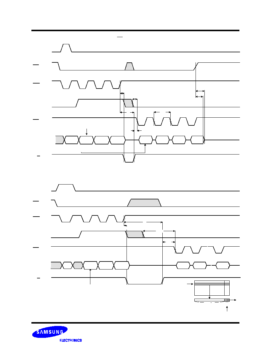
K5D5657DCM-F015
Revision 0.0
June 2003
- 21 -
MCP MEMORY
Preliminary
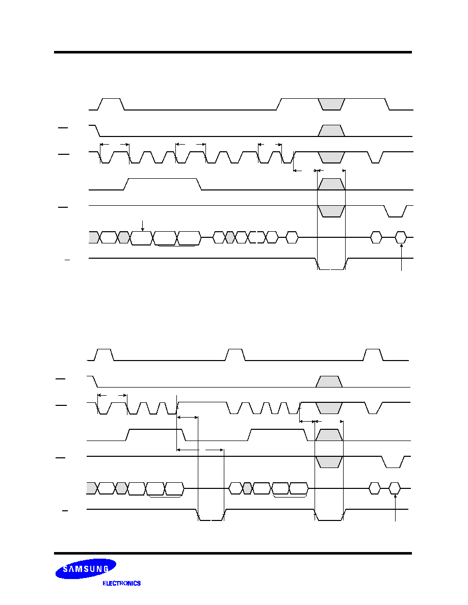
READ1 OPERATION
(INTERCEPTED BY CE)
CE
CLE
R/B
WE
ALE
RE
Busy
Dout N
Dout N+1
Dout N+2
Dout N+3
Page(Row)
Address
Address
Column
t
WB
t
AR
t
CHZ
t
R
t
RR
t
RC
READ2 OPERATION
(READ ONE PAGE)
CE
CLE
R/B
WE
ALE
RE
50h
Dout
Dout 528
M Address
512+M
Dout
512+M+1
Selected
Row
Start
address M
512
16
t
AR
t
R
t
WB
t
RR
A
0
~A
3
are Valid Address & A
4
~A
7
are Don
t
care
N Address
CMD
Read
I/Ox
I/Ox
Col. Add
Row Add1
Row Add2
Col. Add
Row Add1
Row Add2
t
OH
K5D5657DCM-F015
Revision 0.0
June 2003
- 22 -
MCP MEMORY
Preliminary
PAGE PROGRAM OPERATION
CE
CLE
R/B
WE
ALE
RE
80h
70h
I/O
0
Din
N
Din
Din
10h
528
N+1
Sequential Data
Input Command
Column
Address
Page(Row)
Address
1 up to m Data
Serial Input
Program
Command
Read Status
Command
I/O
0
=0 Successful Program
I/O
0
=1 Error in Program
t
PROG
t
WB
t
WC
t
WC
t
WC
N Address
I/Ox
Col. Add
Row Add1
Row Add2
COPY-BACK PROGRAM OPERATION
CE
CLE
R/B
WE
ALE
RE
00h
70h
I/O
0
8Ah
Column
Address
Page(Row)
Address
Program
Command
Read Status
Command
I/O
0
=0 Successful Program
I/O
0
=1 Error in Program
t
PROG
t
WB
t
WC
A
0
~A
7
A
17
~A
24
A
9
~A
16
Column
Address
Page(Row)
Address
Busy
t
WB
t
R
Busy
I/Ox
Col. Add
Row Add1
Row Add2
K5D5657DCM-F015
Revision 0.0
June 2003
- 23 -
MCP MEMORY
Preliminary
BLOCK ERASE OPERATION
(ERASE ONE BLOCK)
CE
CLE
R/B
WE
ALE
RE
60h
Auto Block Erase
Erase Command
Read Status
Command
I/O
0
=1 Error in Erase
DOh
70h
I/O 0
Busy
t
WB
t
BERS
I/O
0
=0 Successful Erase
Page(Row)
Address
t
WC
Setup Command
I/Ox
A9~A16
A17~A24
MANUFACTURE & DEVICE ID READ OPERATION
CE
CLE
WE
ALE
RE
90h
Read ID Command
Maker Code
Device Code
00h
t
REA
Address. 1cycle
t
AR
I/Ox
ECh
75h

K5D5657DCM-F015
Revision 0.0
June 2003
- 24 -
MCP MEMORY
Preliminary
DEVICE OPERATION
PAGE READ
Upon initial device power up, the device defaults to Read1 mode. This operation is also initiated by writing 00h to the command reg-
ister along with three address cycles. Once the command is latched, it does not need to be written for the following page read opera-
tion. Two types of operations are available : random read, serial page read.
The random read mode is enabled when the page address is changed. The 528 bytes of data within the selected page are trans-
ferred to the data registers in less than 10
µ
s(t
R
). The system controller can detect the completion of this data transfer(tR) by analyz-
ing the output of R/B pin. Once the data in a page is loaded into the registers, they may be read out in 50ns cycle time by sequentially
pulsing RE. High to low transitions of the RE clock output the data starting from the selected column address up to the last column
address[column 511/ 527 depending on the state of GND input pin].
The way the Read1 and Read2 commands work is like a pointer set to either the main area or the spare area. The spare area of 512
~527 bytes may be selectively accessed by writing the Read2 command with GND input pin low. Addresses A
0~
A
3
set the starting
address of the spare area while addresses A
4
~A
7
are ignored in X8 device case. The Read1 command is needed to move the pointer
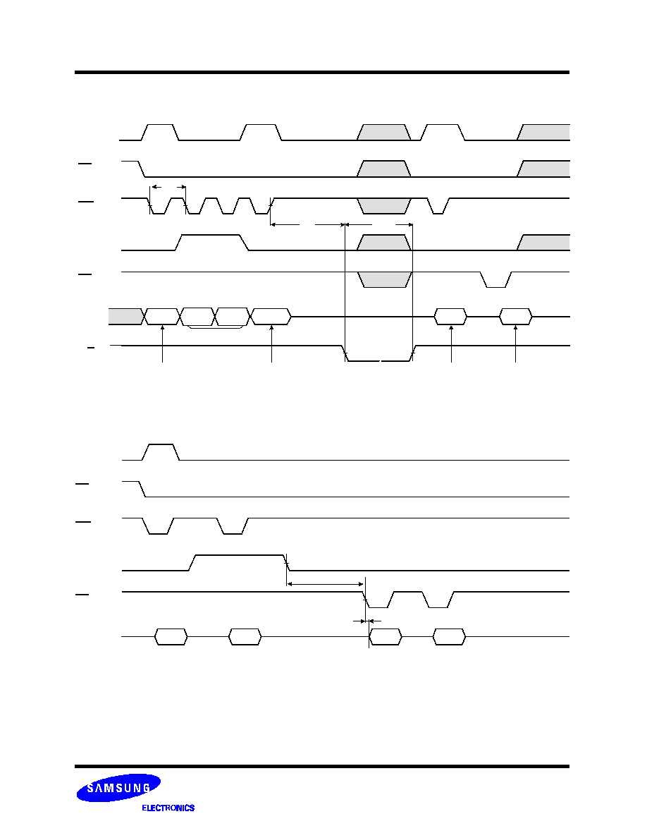
back to the main area. Figures6,7 show typical sequence and timings for each read operation.
Figure 6. Read1 Operation
Start Add.(3Cycle)
00h
A
0
~ A
7
& A
9
~ A
24
Data Output(Sequential)
(00h Command)
Data Field
Spare Field
CE
CLE
ALE
R/B
WE
RE
t
R
Main array
(01h Command)
Data Field
Spare Field
1st half array
2st half array
NOTE
:
1. After data access on 2nd half array by 01h command, the start pointer is automatically moved to 1st half
array (00h) at next cycle.
I/Ox
1)
K5D5657DCM-F015
Revision 0.0
June 2003
- 25 -
MCP MEMORY
Preliminary
Figure 7. Read2 Operation
50h
Data Output(Sequential)
Spare Field
CE
CLE
ALE
R/B
WE
Start Add.(3Cycle)
RE
t
R
A
0
~ A
3
& A
9
~ A
24
Main array
Data Field
Spare Field
A
4
~ A
7
Don't care
I/Ox
K5D5657DCM-F015
Revision 0.0
June 2003
- 26 -
MCP MEMORY
Preliminary
PAGE PROGRAM
The device is programmed basically on a page basis, but it does allow multiple partial page programing of a byte or consecutive bytes
up to 528, in a single page program cycle. The number of consecutive partial page programming operation within the same page with-
out an intervening erase operation should not exceed 2 for main array and 3 for spare array. The addressing may be done in any ran-
dom order in a block. A page program cycle consists of a serial data loading period in which up to 528 bytes of data may be loaded
into the page register, followed by a non-volatile programming period where the loaded data is programmed into the appropriate cell.
About the pointer operation, please refer to the attached technical notes.
The serial data loading period begins by inputting the Serial Data Input command(80h), followed by the three cycle address input and
then serial data loading. The words other than those to be programmed do not need to be loaded.The Page Program confirm com-
mand(10h) initiates the programming process. Writing 10h alone without previously entering the serial data will not initiate the pro-
gramming process. The internal write controller automatically executes the algorithms and timings necessary for program and verify,
thereby freeing the system controller for other tasks. Once the program process starts, the Read Status Register command may be
entered, with RE and CE low, to read the status register. The system controller can detect the completion of a program cycle by mon-
itoring the R/B output, or the Status bit(I/O 6) of the Status Register. Only the Read Status command and Reset command are valid
while programming is in progress. When the Page Program is complete, the Write Status Bit(I/O 0) may be checked(Figure 8). The
internal write verify detects only errors for "1"s that are not successfully programmed to "0"s. The command register remains in Read
Status command mode until another valid command is written to the command register.
Figure 8. Program Operation
80h
R/B
Address & Data Input
I/O
0
Pass
10h
70h
Fail
t
PROG
COPY-BACK PROGRAM
The copy-back program is configured to quickly and efficiently rewrite data stored in one page within the array to another page within
the same array without utilizing an external memory. Since the time-consuming sequently-reading and its re-loading cycles are
removed, the system performance is improved. The benefit is especially obvious when a portion of a block is updated and the rest of
the block also need to be copied to the newly assigned free block. The operation for performing a copy-back is a sequential execution
of page-read without burst-reading cycle and copying-program with the address of destination page. A normal read operation with
"00h" command with the address of the source page moves the whole 528bytes data into the internal buffer. As soon as the Flash
returns to Ready state, copy-back programming command "8Ah" may be given with three address cycles of target page followed. The
data stored in the internal buffer is then programmed directly into the memory cells of the destination page. Once the Copy-Back Pro-
gram is finished, any additional partial page programming into the copied pages is prohibited before erase. Since the memory array is
internally partitioned into two different planes, copy-back program is allowed only within the same memory plane. Thus, A14, the
plane address, of source and destination page address must be the same.
Figure 9. Copy-Back Program Operation
00h
R/B
Add.(3Cycles)
I/O
0
Pass
8Ah
70h
Fail
t
PROG
Add.(3Cycles)
t
R
Source Address
Destination Address
I/Ox
I/Ox
K5D5657DCM-F015
Revision 0.0
June 2003
- 27 -
MCP MEMORY
Preliminary
Figure 10. Block Erase Operation
BLOCK ERASE
The Erase operation is done on a block basis. Block address loading is accomplished in two cycles initiated by an Erase Setup com-
mand(60h). Only address A
14
to A
24
is valid while A
9
to A
13
is ignored. The Erase Confirm command(D0h) following the block address
loading initiates the internal erasing process. This two-step sequence of setup followed by execution command ensures that memory
contents are not accidentally erased due to external noise conditions.
At the rising edge of WE after the erase confirm command input, the internal write controller handles erase and erase-verify. When
the erase operation is completed, the Write Status Bit(I/O 0) may be checked. Figure 10 details the sequence.
60h
Block Add. : A
9
~ A
24
R/B
Address Input(2Cycle)
I/O
0
Pass
D0h
70h
Fail
t
BERS
READ STATUS
The device contains a Status Register which may be read to find out whether program or erase operation is completed, and whether
the program or erase operation is completed successfully. After writing 70h command to the command register, a read cycle outputs
the content of the Status Register to the I/O pins on the falling edge of CE or RE, whichever occurs last. This two line control allows
the system to poll the progress of each device in multiple memory connections even when R/B pins are common-wired. RE or CE
does not need to be toggled for updated status. Refer to table 3 for specific Status Register definitions. The command register
remains in Status Read mode until further commands are issued to it. Therefore, if the status register is read during a random read
cycle, a read command(00h or 50h) should be given before sequential page read cycle.
Table3. Read Status Register Definition
I/O #
Status
Definition
I/O 0
Program / Erase
"0" : Successful Program / Erase
"1" : Error in Program / Erase
I/O 1
Reserved for Future
Use
"0"
I/O 2
"0"
I/O 3
"0"
I/O 4
"0"
I/O 5
"0"
I/O 6
Device Operation
"0" : Busy "1" : Ready
I/O 7
Write Protect
"0" : Protected "1" : Not Protected
I/Ox
K5D5657DCM-F015
Revision 0.0
June 2003
- 28 -
MCP MEMORY
Preliminary
Figure 11. Read ID Operation
CE
CLE
ALE
RE
WE
90h
00h
Address. 1cycle
Maker code
Device code
t
CEA
t
AR
t
REA
READ ID
The device contains a product identification mode, initiated by writing 90h to the command register, followed by an address input of
00h. Two read cycles sequentially output the manufacture code(ECh), and the device code respectively. The command register
remains in Read ID mode until further commands are issued to it. Figure 11 shows the operation sequence.
t
WHR
Figure 12. RESET Operation
RESET
The device offers a reset feature, executed by writing FFh to the command register. When the device is in Busy state during random
read, program or erase mode, the reset operation will abort these operations. The contents of memory cells being altered are no
longer valid, as the data will be partially programmed or erased. The command register is cleared to wait for the next command, and
the Status Register is cleared to value C0h when WP is high. Refer to table 3 for device status after reset operation. If the device is
already in reset state a new reset command will not be accepted by the command register. The R/B pin transitions to low for tRST
after the Reset command is written. Refer to Figure 12 below.
Table4. Device Status
After Power-up
After Reset
Operation Mode
Read 1
Waiting for next command
FFh
R/B
t
RST
ECh
I/Ox
I/Ox
75h

K5D5657DCM-F015
Revision 0.0
June 2003
- 29 -
MCP MEMORY
Preliminary
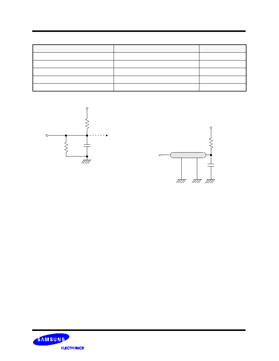
READY/BUSY
The device has a R/B output that provides a hardware method of indicating the completion of a page program, erase and random
read completion. The R/B pin is normally high but transitions to low after program or erase command is written to the command reg-
ister or random read is started after address loading. It returns to high when the internal controller has finished the operation. The pin
is an open-drain driver thereby allowing two or more R/B outputs to be Or-tied. Because pull-up resistor value is related to tr(R/B) and
current drain during busy(ibusy) , an appropriate value can be obtained with the following reference chart. Its value can be deter-
mined by the following guidance.
Vccqn
R/Bn
open drain output
Device
GND
Rp
ibusy
Busy
Ready
Vccqn
Vccqn-0.4V
tf
tr
0.4V
Figure 13. Rp vs tr ,tf & Rp vs ibusy
t
r
,
t
f
[
s
]
I
b
u
s
y
[
A
]
Rp(ohm)
Ibusy
tr
@ Vcc = 2.65V, Ta = 25
∞
C , C
L
= 30pF
1K
2K
3K
4K
100n
200n
300n
3m
2m
1m
30
tf
60
90
120
2.3
2.3
2.3
2.3
2.3
1.1
0.75
0.55
Rp(min, 2.65V part) =
V
CC
(Max.) - V
OL
(Max.)
I
OL
+
I
L
=
2.5V
3mA
+
I
L
where I
L
is the sum of the input currents of all devices tied to the R/B pin.
Rp value guidance
Rp(max) is determined by maximum permissible limit of tr
K5D5657DCM-F015
Revision 0.0
June 2003
- 30 -
MCP MEMORY
Preliminary
The device is designed to offer protection from any involuntary program/erase during power-transitions. An internal voltage detector
disables all functions whenever Vcc is below about 1.8V. WP pin provides hardware protection and is recommended to be kept at V
IL
during power-up and power-down and recovery time of minimum 10
µ
s is required before internal circuit gets ready for any command
sequences as shown in Figure 14. The two step command sequence for program/erase provides additional software protection.
Figure 14. AC Waveforms for Power Transition
V
CC
WP
High
~ 2.0V
WE
Data Protection & Power up sequence
~ 2.0V
10
µ
s

K5D5657DCM-F015
Revision 0.0
June 2003
- 31 -
MCP MEMORY
Preliminary
256Mb(16Mb x 16)
Mobile SDRAM E'-Die
K5D5657DCM-F015
Revision 0.0
June 2003
- 32 -
MCP MEMORY
Preliminary
DC OPERATING CONDITIONS
Recommended operating conditions (Voltage referenced to V
SS
= 0V, T
A
= -25
∞
C ~ 85
∞
C for Extended, -25
∞
C ~ 70
∞
C for Commercial
)
NOTES :
1. VIH (max) = 2.2V AC.The overshoot voltage duration is
3ns.
2. VIL (min) = -1.0V AC. The undershoot voltage duration is
3ns.
3. Any input 0V
VIN
VDDQ.
Input leakage currents include Hi-Z output leakage for all bi-directional buffers with tri-state outputs.
4. Dout is disabled, 0V
VOUT
VDDQ.
Parameter
Symbol
Min
Typ
Max
Unit
Note
Supply voltage
V
DD
1.65
1.8
1.95
V
V
DDQ
1.65
1.8
1.95
V
Input logic high voltage
V
IH
0.8 x V
DDQ
1.8
V
DDQ
+ 0.3
V
1
Input logic low voltage
V
IL
-0.3
0
0.3
V
2
Output logic high voltage
V
OH
V
DDQ
-0.2
-
-
V
I
OH
= -0.1mA
Output logic low voltage
V
OL
-
-
0.2
V
I
OL
= 0.1mA
Input leakage current
I
LI
-10
-
10
uA
3
CAPACITANCE
(V
DD
= 1.8V, T
A
= 23
∞
C, f = 1MHz, V
REF
=0.9V
±
50 mV)
Pin
Symbol
Min
Max
Unit
Note
Clock
C
CLK
TBD
TBD
pF
RAS, CAS, WE, CS, CKE, DQM
C
IN
TBD
TBD
pF
Address
C
ADD
TBD
TBD
pF
DQ
0
~ DQ
15
C
OUT
TBD
TBD
pF
ABSOLUTE MAXIMUM RATINGS
NOTES:
Permanent device damage may occur if ABSOLUTE MAXIMUM RATINGS are exceeded.
Functional operation should be restricted to recommended operating condition.
Exposure to higher than recommended voltage for extended periods of time could affect device reliability.
Parameter
Symbol
Value
Unit
Voltage on any pin relative to V
ss
V
IN
, V
OUT
-1.0 ~ 2.6
V
Voltage on V
DD
supply relative to V
ss
V
DD
, V
DDQ
-1.0 ~ 2.6
V
Storage temperature
T
STG
-55 ~ +150
∞
C
Power dissipation
P
D
1.0
W
Short circuit current
I
OS
50
mA
K5D5657DCM-F015
Revision 0.0
June 2003
- 33 -
MCP MEMORY
Preliminary
DC CHARACTERISTICS
Recommended operating conditions (Voltage referenced to V
SS
= 0V, T
A
= -25
∞
C ~ 85
∞
C for Extended, -25
∞
C ~ 70
∞
C for Commercial)
NOTES:
1. Measured with outputs open.
2. Refresh period is 64ms.
3. Unless otherwise noted, input swing IeveI is CMOS(VIH /VIL=VDDQ/VSSQ).
Parameter
Symbol
Test Condition
Version
Unit
Note
-IL
-15
Operating Current
(One Bank Active)
I
CC1
Burst length = 1
t
RC
t
RC
(min)
I
O
= 0 mA
40
40
mA
1
Precharge Standby Current in
power-down mode
I
CC2
P
CKE
V
IL
(max), t
CC
= 10ns
0.3
mA
I
CC2
PS
CKE & CLK
V
IL
(max), t
CC
=
0.3
Precharge Standby Current
in non power-down mode
I
CC2
N
CKE
V
IH
(min), CS
V
IH
(min), t
CC
= 10ns
Input signals are changed one time during 20ns
10
mA
I
CC2
NS
CKE
V
IH
(min), CLK
V
IL
(max), t
CC
=
Input signals are stable
1
Active Standby Current
in power-down mode
I
CC3
P
CKE
V
IL
(max), t
CC
= 10ns
5
mA
I
CC3
PS
CKE & CLK
V
IL
(max), t
CC
=
1
Active Standby Current
in non power-down mode
(One Bank Active)
I
CC3
N
CKE
V
IH
(min), CS
V
IH
(min), t
CC
= 10ns
Input signals are changed one time during 20ns
20
mA
I
CC3
NS
CKE
V
IH
(min), CLK
V
IL
(max), t
CC
=
Input signals are stable
5
mA
Operating Current
(Burst Mode)
I
CC
4
I
O
= 0 mA
Page burst
4Banks Activated
t
CCD
= 2CLKs
60
50
mA
1
Refresh Current
I
CC
5
t
ARFC
t
ARFC
(min)
65
65
mA
2
Self Refresh Current
I
CC
6
CKE
0.2V
TCSR
Max 40
∞
∞
C
Max 85
∞
∞
C
∞
∞
C
4 Banks
200
480
uA
2 Banks
160
300
1 Bank
130
220
K5D5657DCM-F015
Revision 0.0
June 2003
- 34 -
MCP MEMORY
Preliminary
1.8V
13.9K
10.6K
Output
30pF
VOH (DC) = VDDQ - 0.2V, IOH = -0.1mA
VOL (DC) = 0.2V, IOL = 0.1mA
Vtt=0.5 x VDDQ
50
Output
30pF
Z0=50
Figure 2. AC Output Load Circuit
Figure 1. DC Output Load Circuit
AC OPERATING TEST CONDITIONS
(V
DD
= 1.8V
±
0.15V, T
A
= -25
∞
C ~ 85
∞
C for Extended, -25
∞
C ~ 70
∞
C for Commer-
Parameter
Value
Unit
AC input levels (Vih/Vil)
0.9 x V
DDQ
/ 0.2
V
Input timing measurement reference level
0.5 x V
DDQ
V
Input rise and fall time
tr/tf = 1/1
ns
Output timing measurement reference level
0.5 x V
DDQ
V
Output load condition
See Figure 2
K5D5657DCM-F015
Revision 0.0
June 2003
- 35 -
MCP MEMORY
Preliminary
OPERATING AC PARAMETER
(AC operating conditions unless otherwise noted)
NOTES:
1. The minimum number of clock cycles is determined by dividing the minimum time required with clock cycle time
and then rounding off to the next higher integer.
2. Minimum delay is required to complete write.
3. Minimum 3CLK of tDAL(= tRDL + tRP) is required because it need minimum 2CLK for tRDL and minimum 1CLK for tRP.
4. All parts allow every cycle column address change.
5. In case of row precharge interrupt, auto precharge and read burst stop.
Parameter
Symbol
Version
Unit
Note
-IL
-15
Row active to row active delay
t
RRD
(min)
19
30
ns
1
RAS to CAS delay
t
RCD
(min)
28.5
30
ns
1
Row precharge time
t
RP
(min)
28.5
30
ns
1
Row active time
t
RAS
(min)
60
60
ns
1
t
RAS
(max)
100
us
Row cycle time
t
RC
(min)
88.5
90
ns
1
Last data in to row precharge
t
RDL
(min)
2
CLK
2
Last data in to Active delay
t
DAL
(min)
tRDL + tRP
-
3
Last data in to new col. address delay
t
CDL
(min)
1
CLK
2
Last data in to burst stop
t
BDL
(min)
1
CLK
2
Auto refresh cycle time
t
ARFC
(min)
105
ns
Exit self refresh to active command
t
SRFX
(min)
120
ns
Col. address to col. address delay
t
CCD
(min)
1
CLK
4
Number of valid output data
CAS latency=3
2
ea
5
Number of valid output data
CAS latency=2
1
Number of valid output data
CAS latency=1
0

K5D5657DCM-F015
Revision 0.0
June 2003
- 36 -
MCP MEMORY
Preliminary
AC CHARACTERISTICS
(AC operating conditions unless otherwise noted)
NOTES :
1. Parameters depend on programmed CAS latency.
2. If clock rising time is longer than 1ns, (tr/2-0.5)ns should be added to the parameter.
3. Assumed input rise and fall time (tr & tf) = 1ns.
If tr & tf is longer than 1ns, transient time compensation should be considered,
i.e., [(tr + tf)/2-1]ns should be added to the parameter.
Parameter
Symbol
-1L
-15
Unit
Note
Min
Max
Min
Max
CLK cycle time
CAS latency=3
t
CC
9.5
1000
15
1000
ns
1
CLK cycle time
CAS latency=2
t
CC
15
15
CLK cycle time
CAS latency=1
t
CC
25
30
CLK to valid output delay
CAS latency=3
t
SAC
7
9
ns
1,2
CLK to valid output delay
CAS latency=2
t
SAC
8
9
CLK to valid output delay
CAS latency=1
t
SAC
20
24
Output data hold time
CAS latency=3
t
OH
2.5
2.5
ns
2
Output data hold time
CAS latency=2
t
OH
2.5
2.5
Output data hold time
CAS latency=1
t
OH
2.5
2.5
CLK high pulse width
t
CH
3.5
3.5
ns
3
CLK low pulse width
t
CL
3.5
3.5
ns
3
Input setup time
t
SS
3.0
4.0
ns
3
Input hold time
t
SH
1.5
2.0
ns
3
CLK to output in Low-Z
t
SLZ
1
1
ns
2
CLK to output in Hi-Z
CAS latency=3
t
SHZ
7
9
ns
CAS latency=2
8
9
CAS latency=1
20
24

K5D5657DCM-F015
Revision 0.0
June 2003
- 37 -
MCP MEMORY
Preliminary
SIMPLIFIED TRUTH TABLE
(V=Valid, X=Don
t Care, H=Logic High, L=Logic Low)
NOTES :
1. OP Code : Operand Code
A0 ~ A11 & BA0 ~ BA1 : Program keys. (@MRS)
2. MRS can be issued only at all banks precharge state.
A new command can be issued after 2 CLK cycles of MRS.
3. Auto refresh functions are the same as CBR refresh of DRAM.
The automatical precharge without row precharge command is meant by "Auto".
Auto/self refresh can be issued only at all banks precharge state.
Partial self refresh can be issued only after setting partial self refresh mode of EMRS.
4. BA0 ~ BA1 : Bank select addresses.
5. During burst read or write with auto precharge, new read/write command can not be issued.
Another bank read/write command can be issued after the end of burst.
New row active of the associated bank can be issued at tRP after the end of burst.
6. Burst stop command is valid at every burst length.
7. DQM sampled at the positive going edge of CLK masks the data-in at that same CLK in write operation (Write DQM latency
is 0), but in read operation, it makes the data-out Hi-Z state after 2 CLK cycles. (Read DQM latency is 2).
COMMAND
CKEn-1 CKEn
CS
RAS
CAS
WE
DQM BA0,1 A10/AP
A11,
A9 ~ A0
Note
Register
Mode Register Set
H
X
L
L
L
L
X
OP CODE
1, 2
Refresh
Auto Refresh
H
H
L
L
L
H
X
X
3
Self
Refresh
Entry
L
3
Exit
L
H
L
H
H
H
X
X
3
H
X
X
X
3
Bank Active & Row Addr.
H
X
L
L
H
H
X
V
Row Address
Read &
Column Address
Auto Precharge Disable
H
X
L
H
L
H
X
V
L
Column
Address
(A0~A7)
4
Auto Precharge Enable
H
4, 5
Write &
Column Address
Auto Precharge Disable
H
X
L
H
L
L
X
V
L
Column
Address
(A0~A7)
4
Auto Precharge Enable
H
4, 5
Burst Stop
H
X
L
H
H
L
X
X
6
Precharge
Bank Selection
H
X
L
L
H
L
X
V
L
X
All Banks
X
H
Clock Suspend or
Active Power Down
Entry
H
L
H
X
X
X
X
X
L
V
V
V
Exit
L
H
X
X
X
X
X
Precharge Power Down
Mode
Entry
H
L
H
X
X
X
X
X
L
H
H
H
Exit
L
H
H
X
X
X
X
L
V
V
V
DQM
H
X
V
X
7
No Operation Command
H
X
H
X
X
X
X
X
L
H
H
H
K5D5657DCM-F015
Revision 0.0
June 2003
- 38 -
MCP MEMORY
Preliminary
Register Programmed with Extended MRS
Address
BA1
BA0
A11 ~ A10/AP
A9
A8
A7
A6
A5
A4
A3
A2
A1
A0
Function
Mode Select
RFU
DS
RFU
PASR
Normal MRS Mode
Test Mode
CAS Latency
Burst Type
Burst Length
A8
A7
Type
A6
A5
A4
Latency
A3
Type
A2
A1
A0
BT=0
BT=1
0
0
Mode Register Set
0
0
0
Reserved
0
Sequential
0
0
0
1
1
0
1
Reserved
0
0
1
1
1
Interleave
0
0
1
2
2
1
0
Reserved
0
1
0
2
Mode Select
0
1
0
4
4
1
1
Reserved
0
1
1
3
BA1 BA0
Mode
0
1
1
8
8
Write Burst Length
1
0
0
Reserved
0
0
Setting
for Nor-
mal MRS
1
0
0
Reserved
Reserved
A9
Length
1
0
1
Reserved
1
0
1
Reserved
Reserved
0
Burst
1
1
0
Reserved
1
1
0
Reserved
Reserved
1
Single Bit
1
1
1
Reserved
1
1
1
Full Page
Reserved
Register Programmed with Normal MRS
Address
BA0 ~ BA1
*1
BA0
A11 ~ A10/
AP
A9
*2
A8
A7
A6
A5
A4
A3
A2
A1
A0
Function
"0" Setting for Normal
MRS
RFU
W.B.L
Test Mode
CAS Latency
BT
Burst Length
A. MODE REGISTER FIELD TABLE TO PROGRAM MODES
NOTES:
1.RFU(Reserved for future use) should stay "0" during MRS cycle.
2.If A9 is high during MRS cycle, "Burst Read Single Bit Write" function will be enabled.
Mode Select
Driver Strength
PASR
BA1
BA0
Mode
A6
A5
Driver Strength
A2
A1
A0
# of Banks
0
0
Normal MRS
0
0
Full
0
0
0
4 Banks
0
1
Reserved
0
1
1/2
0
0
1
2 Banks
1
0
EMRS for Mobile SDRAM
1
0
1/4
0
1
0
1 Bank
1
1
Reserved
1
1
1/8
0
1
1
Reserved
Reserved Address
1
0
0
Reserved
A11~A10/AP
A9
A8
A7
A4
A3
1
0
1
Reserved
0
0
0
0
0
0
1
1
0
Reserved
1
1
1
Reserved
EMRS for PASR(Partial Array Self Ref.) & DS(Driver Strength)
Full Page Length x16 : 64Mb(256), 128Mb(512),256Mb(512),512Mb(1024)

K5D5657DCM-F015
Revision 0.0
June 2003
- 39 -
MCP MEMORY
Preliminary
1. In order to save power consumption, Mobile SDRAM has PASR option.
2. Mobile SDRAM supports 3 kinds of PASR in self refresh mode : 4 Banks, 2 Banks and 1 Bank.
BA1=0
- 4 Banks
- 2 Banks
- 1 Bank
Partial Self Refresh Area
1. Apply power and attempt to maintain CKE at a high state and all other inputs may be undefined.
- Apply VDD before or at the same time as VDDQ.
2. Maintain stable power, stable clock and NOP input condition for a minimum of 200us.
3. Issue precharge commands for all banks of the devices.
4. Issue 2 or more auto-refresh commands.
5. Issue a mode register set command to initialize the mode register.
6. Issue a extended mode register set command to define DS or PASR operating type of the device after normal MRS.
EMRS cycle is not mandatory and the EMRS command needs to be issued only when DS or PASR is used.
The default state without EMRS command issued is half driver strength, all 4 banks refreshed.
The device is now ready for the operation selected by EMRS.
For operating with DS or PASR , set DS or PASR mode in EMRS setting stage.
In order to adjust another mode in the state of DS or PASR mode, additional EMRS set is required but power up sequence is not
needed again at this time. In that case, all banks have to be in idle state prior to adjusting EMRS set.
BA0=0
BA1=0
BA0=0
BA1=0
BA0=1
BA1=1
BA0=1
BA1=1
BA0=0
BA1=1
BA0=1
BA1=1
BA0=0
BA1=0
BA0=1
BA1=0
BA0=0
BA1=0
BA0=1
BA1=1
BA0=1
BA1=1
BA0=0
Partial Array Self Refresh
B. POWER UP SEQUENCE
Note :
1. In order to save power consumption, Mobile DDR SDRAM includes the internal temperature sensor and control units to control the
self refresh cycle automatically according to the two temperature range ; Max. 40
∞
C, Max. 85
∞
C.
2. If the EMRS for external TCSR is issued by the controller, this EMRS code for TCSR is ignored.
Temperature Range
Self Refresh Current (Icc 6)
Unit
4 Banks
2 Banks
1 Bank
Max. 40
∞
C
200
160
130
uA
Max. 85
∞
C
480
300
220
Internal Temperature Compensated Self Refresh (TCSR)
K5D5657DCM-F015
Revision 0.0
June 2003
- 40 -
MCP MEMORY
Preliminary
C. BURST SEQUENCE
1. BURST LENGTH = 4
Initial Address
Sequential
Interleave
A1
A0
0
0
0
1
2
3
0
1
2
3
0
1
1
2
3
0
1
0
3
2
1
0
2
3
0
1
2
3
0
1
1
1
3
0
1
2
3
2
1
0
2. BURST LENGTH = 8
Initial Address
Sequential
Interleave
A2
A1
A0
0
0
0
0
1
2
3
4
5
6
7
0
1
2
3
4
5
6
7
0
0
1
1
2
3
4
5
6
7
0
1
0
3
2
5
4
7
6
0
1
0
2
3
4
5
6
7
0
1
2
3
0
1
6
7
4
5
0
1
1
3
4
5
6
7
0
1
2
3
2
1
0
7
6
5
4
1
0
0
4
5
6
7
0
1
2
3
4
5
6
7
0
1
2
3
1
0
1
5
6
7
0
1
2
3
4
5
4
7
6
1
0
3
2
1
1
0
6
7
0
1
2
3
4
5
6
7
4
5
2
3
0
1
1
1
1
7
0
1
2
3
4
5
6
7
6
5
4
3
2
1
0

K5D5657DCM-F015
Revision 0.0
June 2003
- 41 -
MCP MEMORY
Preliminary
BANK ADDRESSES (BA0 ~ BA1)
: In case x 16
This SDRAM is organized as four independent banks of
4,194,304 words x 16 bits memory arrays. The BA0 ~ BA1 inputs
are latched at the time of assertion of RAS and CAS to select the
bank to be used for the operation. The bank addresses BA0 ~
BA1 are latched at bank active, read, write, mode register set
and precharge operations.
: In case x 32
This SDRAM is organized as four independent banks of
2,097,152 words x 32 bits memory arrays. The BA0 ~ BA1 inputs
are latched at the time of assertion of RAS and CAS to select the
bank to be used for the operation. The bank addresses BA0 ~
BA1 are latched at bank active, read, write, mode register set
and precharge operations.
ADDRESS INPUTS (A0 ~ A12)
: In case x 16
The 22 address bits are required to decode the 4,194,304 word
locations are multiplexed into 13 address input pins (A0 ~ A12).
The 13 bit row addresses are latched along with RAS and BA0 ~
BA1 during bank activate command. The 9 bit column addresses
are latched along with CAS, WE and BA0 ~ BA1 during read or
write command.
: In case x 32
The 21 address bits are required to decode the 2,097,152 word
locations are multiplexed into 12 address input pins (A0 ~ A11).
The 12 bit row addresses are latched along with RAS and BA0 ~
BA1 during bank activate command. The 9 bit column addresses
are latched along with CAS, WE and BA0 ~ BA1 during read or
write command.
BANK ADDRESSES (BA0 ~ BA1)
: In case x 16
This SDRAM is organized as four independent banks of
8,388,608 words x 16 bits memory arrays. The BA0 ~ BA1 inputs
are latched at the time of assertion of RAS and CAS to select the
bank to be used for the operation. The bank addresses BA0 ~
BA1 are latched at bank active, read, write, mode register set
and precharge operations.
: In case x 32
This SDRAM is organized as four independent banks of
4,194,304 words x 32 bits memory arrays. The BA0 ~ BA1 inputs
are latched at the time of assertion of RAS and CAS to select the
bank to be used for the operation. The bank addresses BA0 ~
BA1 are latched at bank active, read, write, mode register set
and precharge operations.
ADDRESS INPUTS (A0 ~ A12)
: In case x 16
The 23 address bits are required to decode the 8,388,608 word
locations are multiplexed into 13 address input pins (A0 ~ A12).
The 13 bit row addresses are latched along with RAS and BA0 ~
BA1 during bank activate command. The 10 bit column
addresses are latched along with CAS, WE and BA0 ~ BA1 dur-
ing read or write command.
: In case x 32
The 22 address bits are required to decode the 8,388,608 word
locations are multiplexed into 13 address input pins (A0 ~ A12).
The 13 bit row addresses are latched along with RAS and BA0 ~
BA1 during bank activate command. The 9 bit column addresses
are latched along with CAS, WE and BA0 ~ BA1 during read or
write command.
ADDRESSES of 256Mb
ADDRESSES of 512Mb
D. DEVICE OPERATIONS

K5D5657DCM-F015
Revision 0.0
June 2003
- 42 -
MCP MEMORY
Preliminary
CLOCK (CLK)
The clock input is used as the reference for all SDRAM opera-
tions. All operations are synchronized to the positive going edge
of the clock. The clock transitions must be monotonic between
V
IL
and V
IH
. During operation with CKE high all inputs are
assumed to be in a valid state (low or high) for the duration of
set-up and hold time around positive edge of the clock in order to
function well Q perform and ICC specifications.
CLOCK ENABLE (CKE)
The clock enable(CKE) gates the clock onto SDRAM. If CKE
goes low synchronously with clock (set-up and hold time are the
same as other inputs), the internal clock is suspended from the
next clock cycle and the state of output and burst address is fro-
zen as long as the CKE remains low. All other inputs are ignored
from the next clock cycle after CKE goes low. When all banks are
in the idle state and CKE goes low synchronously with clock, the
SDRAM enters the power down mode from the next clock cycle.
The SDRAM remains in the power down mode ignoring the other
inputs as long as CKE remains low. The power down exit is syn-
chronous as the internal clock is suspended. When CKE goes
high at least "1CLK + tSS" before the high going edge of the
clock, then the SDRAM becomes active from the same clock
edge accepting all the input commands.
NOP and DEVICE DESELECT
When RAS, CAS and WE are high, the SDRAM performs no
operation (NOP). NOP does not initiate any new operation, but is
needed to complete operations which require more than single
clock cycle like bank activate, burst read, auto refresh, etc. The
device deselect is also a NOP and is entered by asserting CS
high. CS high disables the command decoder so that RAS, CAS,
WE and all the address inputs are ignored.
DQM OPERATION
The DQM is used to mask input and output operations. It works
similar to OE during read operation and inhibits writing during
write operation. The read latency is two cycles from DQM and
zero cycle for write, which means DQM masking occurs two
cycles later in read cycle and occurs in the same cycle during
write cycle. DQM operation is synchronous with the clock. The
DQM signal is important during burst interruptions of write with
read or precharge in the SDRAM. Due to asynchronous nature of
the internal write, the DQM operation is critical to avoid unwanted
or incomplete writes when the complete burst write is not
required. Please refer to DQM timing diagram also.
MODE REGISTER SET (MRS)
The mode register stores the data for controlling the various
operating modes of SDRAM. It programs the CAS latency, burst
type, burst length, test mode and various vendor specific options
to make SDRAM useful for variety of different applications. The
default value of the mode register is not defined, therefore the
mode register must be written after power up to operate the
SDRAM. The mode register is written by asserting low on CS,
RAS, CAS and WE (The SDRAM should be in active mode with
CKE already high prior to writing the mode register). The state of
address pins A0 ~ An and BA0 ~ BA1 in the same cycle as CS,
RAS, CAS and WE going low is the data written in the mode reg-
ister. Two clock cycles is required to complete the write in the
mode register. The mode register contents can be changed
using the same command and clock cycle requirements during
operation as long as all banks are in the idle state. The mode
register is divided into various fields depending on the fields of
functions. The burst length field uses A0 ~ A2, burst type uses
A3, CAS latency (read latency from column address) use A4 ~
A6, vendor specific options or test mode use A7 ~ A8, A10/AP ~
An and BA0 ~ BA1. The write burst length is programmed using
A9. A7 ~ A8, A10/AP ~ An and BA0 ~ BA1 must be set to low for
normal SDRAM operation. Refer to the table for specific codes
for various burst length, burst type and CAS latencies.
D. DEVICE OPERATIONS (continued)

K5D5657DCM-F015
Revision 0.0
June 2003
- 43 -
MCP MEMORY
Preliminary
EXTENDED MODE REGISTER SET (EMRS)
The extended mode register stores the data for selecting driver
strength and partial self refresh. EMRS cycle is not mandatory
and the EMRS command needs to be issued only when DS or
PASR is used. The default state without EMRS command issued
is half driver strength and all 4 banks refreshed. The extended
mode register is written by asserting low on CS, RAS, CAS, WE
and high on BA1 ,low on BA0(The SDRAM should be in all bank
precharge with CKE already high prior to writing into the
extended mode register). The state of address pins A0 ~ A11 in
the same cycle as CS, RAS, CAS and WE going low is written in
the extended mode register. Two clock cycles are required to
complete the write operation in the extended mode register. The
mode register contents can be changed using the same com-
mand and clock cycle requirements during operation as long as
all banks are in the idle state. A0 - A2 are used for partial self
refresh , A5 - A6 are used for Driver strength, "Low" on BA1 and
"High" on BA0 are used for EMRS. All the other address pins
except A0,A1,A2, BA1, BA0 must be set to low for proper EMRS
operation. Refer to the table for specific codes.
BANK ACTIVATE.
The bank activate command is used to select a random row in an
idle bank. By asserting low on RAS and CS with desired row and
bank address, a row access is initiated. The read or write opera-
tion can occur after a time delay of t
RCD
(min) from the time of
bank activation. t
RCD
is an internal timing parameter of SDRAM,
therefore it is dependent on operating clock frequency. The mini-
mum number of clock cycles required between bank activate and
read or write command should be calculated by dividing
t
RCD
(min) with cycle time of the clock and then rounding off the
result to the next higher integer.
The SDRAM has four internal banks in the same chip and shares
part of the internal circuitry to reduce chip area, therefore it
restricts the activation of four banks simultaneously. Also the
noise generated during sensing of each bank of SDRAM is high,
requiring some time for power supplies to recover before another
bank can be sensed reliably. t
RRD
(min) specifies the minimum
time required between activating different bank. The number of
clock cycles required between different bank activation must be
calculated similar to t
RCD
specification. The minimum time
required for the bank to be active to initiate sensing and restoring
the complete row of dynamic cells is determined by t
RAS
(min).
Every SDRAM bank activate command must satisfy t
RAS
(min)
specification before a precharge command to that active bank
can be asserted. The maximum time any bank can be in the
active state is determined by t
RAS
(max). The number of cycles for
both t
RAS
(min) and t
RAS
(max) can be calculated similar to t
RCD
specification.
BURST READ
The burst read command is used to access burst of data on con-
secutive clock cycles from an active row in an active bank. The
burst read command is issued by asserting low on CS and CAS
with WE being high on the positive edge of the clock. The bank
must be active for at least t
RCD
(min) before the burst read com-
mand is issued. The first output appears in CAS latency number
of clock cycles after the issue of burst read command. The burst
length, burst sequence and latency from the burst read command
is determined by the mode register which is already pro-
grammed. The burst read can be initiated on any column address
of the active row. The address wraps around if the initial address
does not start from a boundary such that number of outputs from
each I/O are equal to the burst length programmed in the mode
register. The output goes into high-impedance at the end of the
burst, unless a new burst read was initiated to keep the data out-
put gapless. The burst read can be terminated by issuing another
burst read or burst write in the same bank or the other active
bank or a precharge command to the same bank. The burst stop
command is valid at every page burst length.
D. DEVICE OPERATIONS (continued)

K5D5657DCM-F015
Revision 0.0
June 2003
- 44 -
MCP MEMORY
Preliminary
BURST WRITE
The burst write command is similar to burst read command and
is used to write data into the SDRAM on consecutive clock
cycles in adjacent addresses depending on burst length and
burst sequence. By asserting low on CS, CAS and WE with valid
column address, a write burst is initiated. The data inputs are
provided for the initial address in the same clock cycle as the
burst write command. The input buffer is deselected at the end of
the burst length, even though the internal writing can be com-
pleted yet. The writing can be completed by issuing a burst read
and DQM for blocking data inputs or burst write in the same or
another active bank. The burst stop command is valid at every
burst length. The write burst can also be terminated by using
DQM for blocking data and procreating the bank t
RDL
after the
last data input to be written into the active row. See DQM
OPERATION also.
ALL BANKS PRECHARGE
All banks can be precharged at the same time by using Pre-
charge all command. Asserting low on CS, RAS, and WE with
high on A10/AP after all banks have satisfied t
RAS
(min) require-
ment, performs precharge on all banks. At the end of t
RP
after
performing precharge to all the banks, all banks are in idle state.
PRECHARGE
The precharge operation is performed on an active bank by
asserting low on CS, RAS, WE and A10/AP with valid BA0 ~ BA1
of the bank to be precharged. The precharge command can be
asserted anytime after t
RAS
(min) is satisfied from the bank active
command in the desired bank. t
RP
is defined as the minimum
number of clock cycles required to complete row precharge is
calculated by dividing t
RP
with clock cycle time and rounding up
to the next higher integer. Care should be taken to make sure
that burst write is completed or DQM is used to inhibit writing
before precharge command is asserted. The maximum time any
bank can be active is specified by t
RAS
(max). Therefore, each
bank activate command. At the end of precharge, the bank
enters the idle state and is ready to be activated again. Entry to
Power down, Auto refresh, Self refresh and Mode register set
etc. is possible only when all banks are in idle state.
AUTO PRECHARGE
The precharge operation can also be performed by using auto
precharge. The SDRAM internally generates the timing to satisfy
t
RAS
(min) and "t
RP
" for the programmed burst length and CAS
latency. The auto precharge command is issued at the same
time as burst read or burst write by asserting high on A10/AP. If
burst read or burst write by asserting high on A10/AP, the bank is
left active until a new command is asserted. Once auto pre-
charge command is given, no new commands are possible to
that particular bank until the bank achieves idle state.
AUTO REFRESH
The storage cells of 64Mb, 128Mb, 256Mb and 512Mb SDRAM
need to be refreshed every 64ms to maintain data. An auto
refresh cycle accomplishes refresh of a single row of storage
cells. The internal counter increments automatically on every
auto refresh cycle to refresh all the rows. An auto refresh com-
mand is issued by asserting low on CS, RAS and CAS with high
on CKE and WE. The auto refresh command can only be
asserted with all banks being in idle state and the device is not in
power down mode (CKE is high in the previous cycle). The time
required to complete the auto refresh operation is specified by
t
RC
(min). The minimum number of clock cycles required can be
calculated by driving t
RC
with clock cycle time and them rounding
up to the next higher integer. The auto refresh command must be
followed by NOP's until the auto refresh operation is completed.
All banks will be in the idle state at the end of auto refresh opera-
tion. The auto refresh is the preferred refresh mode when the
SDRAM is being used for normal data transactions. The 64Mb
and 128Mb SDRAM's auto refresh cycle can be performed once
in 15.6us or a burst of 4096 auto refresh cycles once in 64ms.
The 256Mb and 512Mb SDRAM's auto refresh cycle can be per-
formed once in 7.8us or a burst of 8192 auto refresh cycles once
in 64ms.
D. DEVICE OPERATIONS (continued)

K5D5657DCM-F015
Revision 0.0
June 2003
- 45 -
MCP MEMORY
Preliminary
SELF REFRESH
The self refresh is another refresh mode available in the
SDRAM. The self refresh is the preferred refresh mode for data
retention and low power operation of SDRAM. In self refresh
mode, the SDRAM disables the internal clock and all the input
buffers except CKE. The refresh addressing and timing are inter-
nally generated to reduce power consumption.
The self refresh mode is entered from all banks idle state by
asserting low on CS, RAS, CAS and CKE with high on WE. Once
the self refresh mode is entered, only CKE state being low mat-
ters, all the other inputs including the clock are ignored in order
to remain in the self refresh mode.
The self refresh is exited by restarting the external clock and then
asserting high on CKE. This must be followed by NOP's for a
minimum time of tSRFX before the SDRAM reaches idle state to
begin normal operation. In case that the system uses burst auto
refresh during normal operation, it is recommended to use burst
8192 auto refresh cycles for 256Mb and 512Mb, and burst 4096
auto refresh cycles for 128Mb and 64Mb immediately before
entering self refresh mode and after exiting in self refresh mode.
On the other hand, if the system uses the distributed auto
refresh, the system only has to keep the refresh duty cycle.
D. DEVICE OPERATIONS
(continued)
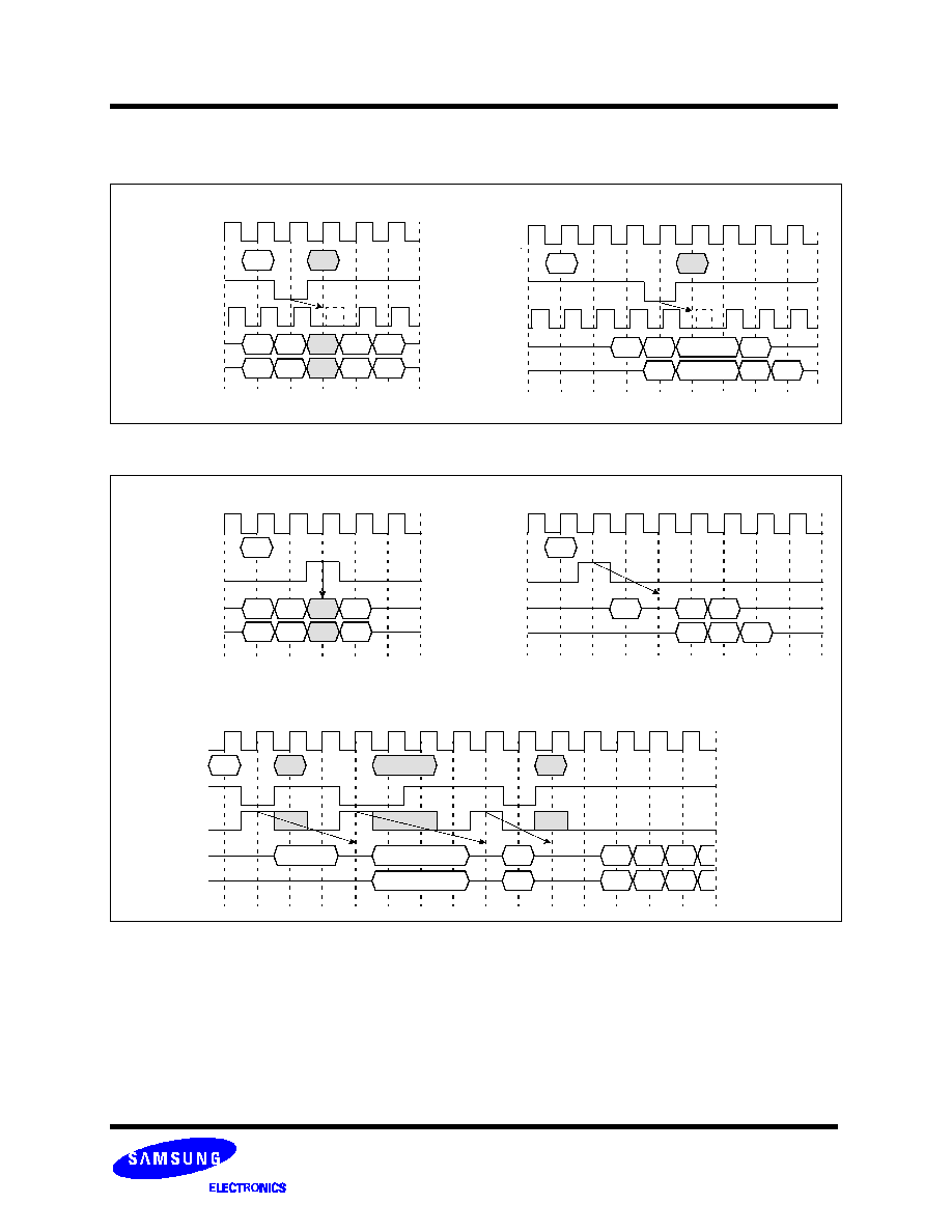
K5D5657DCM-F015
Revision 0.0
June 2003
- 46 -
MCP MEMORY
Preliminary
D
Hi-Z
Hi-Z
Hi-Z
Hi-Z
Hi-Z
Hi-Z
Hi-Z
Hi-Z
*NOTE :
1. CKE to CLK disable/enable = 1CLK.
2. DQM makes data out Hi-Z after 2CLKs which should masked by CKE " L"
3. DQM masks both data-in and data-out.
E. BASIC FEATURE AND FUNCTION DESCRIPTIONS
1. CLOCK Suspend
2. DQM Operation
1) Clock Suspended During Write
CLK
CMD
CKE
Internal
CLK
DQ(CL2)
DQ(CL3)
WR
D
0
D
1
D
2
D
3
D
0
D
1
D
2
D
3
Not Written
Suspended Dout
2) Clock Suspended During Read (BL=4)
CLK
CMD
CKE
Internal
CLK
DQ(CL2)
DQ(CL3)
RD
Masked by CKE
Q
0
Q
1
Q
2
Q
3
Q
0
Q
1
Q
2
Q
3
Masked by CKE
1) Write Mask (BL=4)
2) Read Mask (BL=4)
CLK
CMD
DQM
DQ(CL2)
DQ(CL3)
CLK
CMD
DQM
DQ(CL2)
DQ(CL3)
WR
Masked by CKE
Masked by CKE
D
0
D
1
D
3
D
0
D
1
D
3
RD
Q
0
Q
2
Q
3
Q
1
Q
2
Q
3
DQM to Data-in Mask = 0
DQM to Data-out Mask = 2
3) DQM with Clock Suspended (Full Page Read)
*2
CLK
CMD
CKE
DQM
DQ(CL2)
DQ(CL3)
RD
Q
0
Q
2
Q
4
Q
6
Q
7
Q
8
Q
1
Q
3
Q
6
Q
7
Q
5

K5D5657DCM-F015
Revision 0.0
June 2003
- 47 -
MCP MEMORY
Preliminary
tCCD
*2
tCCD
*2
tCDL
*3
tCCD
*2
tCDL
*3
*NOTE:
1. By " Interrupt", It is meant to stop burst read/write by external command before the end of burst.
By "CAS Interrupt", to stop burst read/write by CAS access ; read and write.
2. t
CCD
: CAS to CAS delay. (=1CLK)
3. t
CDL
: Last data in to new column address delay. (=1CLK)
DQ(CL2)
DQ(CL3)
3. CAS Interrupt (I)
1) Read interrupted by Read (BL=4)
*1
2) Write interrupted by Write (BL=2)
CLK
CMD
ADD
RD
RD
A
B
3) Write interrupted by Read (BL=2)
QA
0
QB
0
QB
1
QB
1
QB
3
QA
0
QB
0
QB
1
QB
1
QB
3
CLK
CMD
ADD
DQ
WR
WR
A
B
DA
0
DB
0
DB
1
CLK
CMD
ADD
DQ(CL2)
DQ(CL3)
WR
RD
A
B
DA
0
QB
0
QB
1
DA
0
QB
0
QB
1
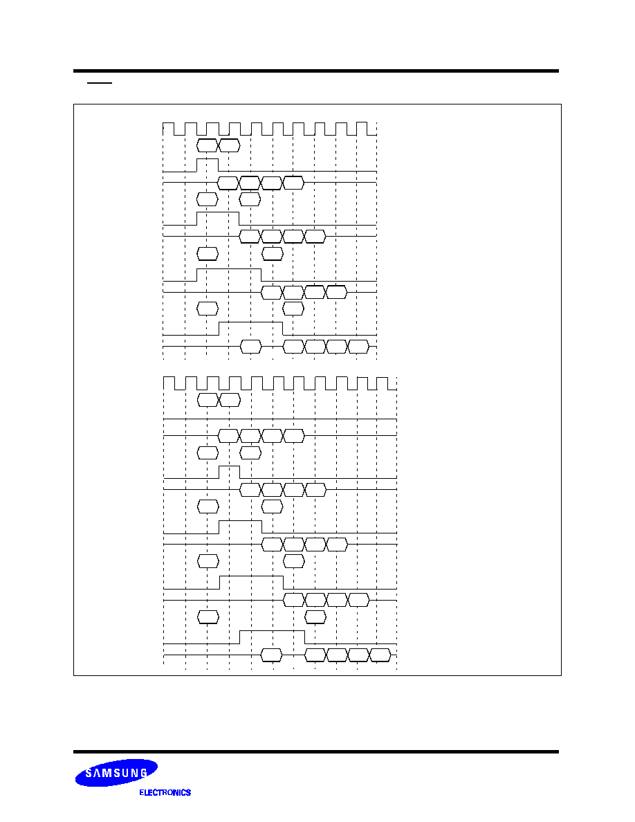
K5D5657DCM-F015
Revision 0.0
June 2003
- 48 -
MCP MEMORY
Preliminary
*NOTE:
1. To prevent bus contention, there should be at least one gap between data in and data out.
Hi-Z
Hi-Z
*1
Hi-Z
Hi-Z
*1
Hi-Z
4. CAS Interrupt (II) : Read Interrupted by Write & DQM
ii) CMD
DQM
(a) CL=2, BL=4
i) CMD
DQ
CLK
DQM
DQ
iii) CMD
DQM
DQ
iv) CMD
DQM
DQ
(b) CL=3, BL=4
CLK
i) CMD
DQM
DQ
ii) CMD
DQM
DQ
iii) CMD
DQM
DQ
iv) CMD
DQM
DQ
v) CMD
DQ
DQM
RD
WR
D
0
D
1
D
2
D
3
RD
WR
D
0
D
1
D
2
D
3
RD
WR
D
0
D
1
D
2
D
3
RD
WR
Q
0
D
0
D
1
D
2
D
3
RD
WR
D
0
D
1
D
2
D
3
RD
WR
D
0
D
1
D
2
D
3
RD
WR
D
0
D
1
D
2
D
3
RD
WR
D
0
D
1
D
2
D
3
RD
WR
D
0
D
1
D
2
D
3
Q
0
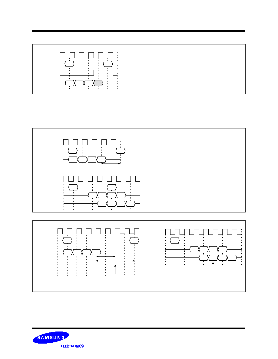
K5D5657DCM-F015
Revision 0.0
June 2003
- 49 -
MCP MEMORY
Preliminary
tRDL =2CLK
tDAL =tRDL + tRP
*4
*NOTE:
1. To prevent bus contention, DQM should be issued which makes at least one gap between data in and data out.
2. To inhibit invalid write, DQM should be issued.
3. This precharge command and burst write command should be of the same bank, otherwise it is not precharge interrupt but only another bank pre-
charge of four banks operation.
tRDL
*1
1
2
*NOTE:
1. SAMSUNG can support tRDL=1CLK and tRDL=2CLK for all memory devices. SAMSUNG recommends tRDL=2 CLK.
2. Number of valid output data after row precharge : 1, 2 for CAS Latency = 2, 3 respectively.
3. The row active command of the precharge bank can be issued after tRP from this point.
The new read/write command of other activated bank can be issued from this point.
At burst read/write with auto precharge, CAS interrupt of the same bank is illegal
4. tDAL defined Last data in to Active delay. SAMSUNG can support tDAL=tRDL+ tRP .
Auto Precharge Starts
*3
*2
*3
*2
5. Write Interrupted by Precharge & DQM
6. Precharge
7. Auto Precharge
1) tRDL = 2CLK
CMD
DQ
CLK
DQM
WR
PRE
D
0
D
1
D
2
Masked by DQM
1) Normal Write
CMD
DQ
CLK
BL=4 & tRDL=2CLK
D
0
D
1
D
2
D
3
WR
PRE
2) Normal Read (BL=4)
CLK
CMD
DQ(CL2)
DQ(CL3)
RD
PRE
Q
0
Q
1
Q
2
Q
3
Q
0
Q
1
Q
2
Q
3
1) Normal Write (BL=4)
CLK
CMD
DQ
WR
Auto Precharge Starts@tRDL=2CLK
*3
D
0
D
1
D
2
D
3
ACT
2) Normal Read (BL=4)
CLK
CMD
DQ(CL2)
DQ(CL3)
RD
Q
0
Q
1
Q
2
Q
3
Q
0
Q
1
Q
2
Q
3
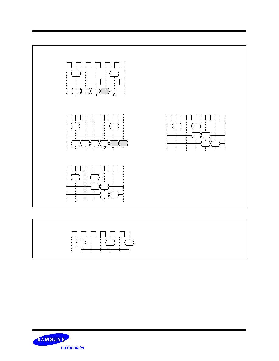
K5D5657DCM-F015
Revision 0.0
June 2003
- 50 -
MCP MEMORY
Preliminary
*NOTE:
1. SAMSUNG can support tRDL=2 CLK.
2. tBDL : 1 CLK ; Last data in to burst stop delay.
Read or write burst stop command is valid at every burst length.
3. Number of valid output data after row precharge or burst stop : 1, 2 for CAS latency= 2, 3 respectively.
4. PRE : All banks precharge is necessary.
MRS can be issued only at all banks precharge state.
1
2
1
2
*4
tRP
2CLK
tRDL
*1
tBDL
*2
8. Burst Stop & Interrupted by Precharge
9. MRS
1) Normal Write
D
0
D
1
D
2
2) Write Burst Stop (BL=8)
CMD
DQ
CLK
DQM
BL=4 & tRDL=2CLK
WR
PRE
CLK
CMD
DQM
DQ
WR
STOP
D
0
D
1
D
2
D
3
3) Read Interrupted by Precharge (BL=4)
CLK
CMD
DQ(CL2)
DQ(CL3)
RD
PRE
Q
0
Q
1
Q
0
Q
1
4) Read Burst Stop (BL=4)
CLK
CMD
DQ(CL2)
DQ(CL3)
RD
STOP
Q
0
Q
1
Q
0
Q
1
1) Mode Register Set
CLK
CMD
PRE
MRS
ACT

K5D5657DCM-F015
Revision 0.0
June 2003
- 51 -
MCP MEMORY
Preliminary
tSS
*1
tSS
*2
Auto Refresh
Command
PRE
t
RP
t
ARFC(min) = 105ns
Auto
CKE = High
Refresh
CMD
An auto refresh command is issued by having CS, RAS and CAS held low with CKE and WE high at the rising edge of the
clock(CLK). All banks must be precharged and idle for t
RP
(min) before the auto refresh command is applied. No control of the external
address pins is required once this cycle has started because of the internal address counter. When the refresh cycle has completed,
all banks will be in the idle state. A delay between the auto refresh command and the next activate command or subsequent auto
refresh command must be greater than or equal to the t
ARFC
(min).
CLK
A Self Refresh command is defined by having CS, RAS, CAS and CKE held low with WE high at the rising edge of the clock. Once
the self Refresh command is initiated, CKE must be held low to keep the device in Self Refresh mode. After 1 clock cycle from the self
refresh command, all of the external control signals including system clock(CLK) can be disabled except CKE. The clock is internally
disabled during Self Refresh operation to reduce power. To exit the Self Refresh mode, supply stable clock input before returning
CKE high, assert deselect or NOP command and then assert CKE high. In case that the system uses burst auto refresh during normal
opreation, it is recommended to use burst 4096 auto refresh cycle immediately before entering self refresh mode and after exiting in
self refresh mode. On the other hand, if the system uses the distributed auto refresh, the system only has to keep the refresh duty
cycle.
Self Refresh
Command
CKE
Stable Clock
t
SS
NOP
Self
Refresh
CLK
t
SRFX(min) = 120ns
t
SS
ACT
10. Clock Suspend Exit & Power Down Exit
11. Auto Refresh & Self Refresh
1) Clock Suspend (=Active Power Down) Exit
2) Power Down (=Precharge Power Down) Exit
CLK
CKE
Internal
CLK
CMD
RD
CLK
CKE
Internal
CLK
CMD
NOP ACT
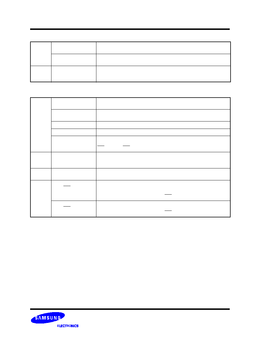
K5D5657DCM-F015
Revision 0.0
June 2003
- 52 -
MCP MEMORY
Preliminary
12. About Burst Type Control
Basic
MODE
Sequential Counting
At MRS A
3
= "0". See the BURST SEQUENCE TABLE. (BL=4, 8)
BL=1, 2, 4, 8 and full page.
Interleave Counting
At MRS A
3
= "1". See the BURST SEQUENCE TABLE. (BL=4, 8)
BL=4, 8. At BL=1, 2 Interleave Counting = Sequential Counting.
Random
MODE
Random column Access
t
CCD
= 1 CLK
Every cycle Read/Write Command with random column address can realize Random
Column Access.
That is similar to Extended Data Out (EDO) Operation of conventional DRAM.
13. About Burst Length Control
Basic
MODE
1
At MRS A
2,1,0
= "000".
At auto precharge, t
RAS
should not be violated.
2
At MRS A
2,1,0
= "001".
At auto precharge, t
RAS
should not be violated.
4
At MRS A
2,1,0
= "010".
8
At MRS A
2,1,0
= "011".
Full Page
At MRS A
2,1,0
= "111".
Wrap around mode(infinite burst length) should be stopped by burst stop.
RAS interrupt or CAS interrupt.
Special
MODE
BRSW
At MRS A
9
= "1".
Read burst =1, 2, 4, 8, full page write Burst =1.
At auto precharge of write, t
RAS
should not be violated.
Random
MODE
Burst Stop
t
BDL
= 1, Valid DQ after burst stop is 1, 2 for CAS latency 2, 3 respectively
Using burst stop command, any burst length control is possible.
Interrupt
MODE
RAS Interrupt
(Interrupted by Precharge)
Before the end of burst, Row precharge command of the same bank stops read/write
burst with Row precharge.
t
RDL
= 2 with DQM, valid DQ after burst stop is 1, 2 for CAS latency 2, 3 respectively.
During read/write burst with auto precharge, RAS interrupt can not be issued.
CAS Interrupt
Before the end of burst, new read/write stops read/write burst and starts new
read/write burst.
During read/write burst with auto precharge, CAS interrupt can not be issued.

K5D5657DCM-F015
Revision 0.0
June 2003
- 53 -
MCP MEMORY
Preliminary
FUNCTION TRUTH TABLE (TABLE 1)
Current
State
CS
RAS
CAS
WE
BA
Address
Action
Note
IDLE
H
X
X
X
X
X
NOP
L
H
H
H
X
X
NOP
L
H
H
L
X
X
ILLEGAL
2
L
H
L
X
BA
CA, A
10
/AP ILLEGAL
2
L
L
H
H
BA
RA
Row (& Bank) Active ; Latch RA
L
L
H
L
BA
A
10
/AP
NOP
4
L
L
L
H
X
X
Auto Refresh or Self Refresh
5
L
L
L
L
OP code
OP code
Mode Register Access
5
Row
Active
H
X
X
X
X
X
NOP
L
H
H
H
X
X
NOP
L
H
H
L
X
X
ILLEGAL
2
L
H
L
H
BA
CA, A
10
/AP Begin Read ; latch CA ; determine AP
L
H
L
L
BA
CA, A
10
/AP Begin Read ; latch CA ; determine AP
L
L
H
H
BA
RA
ILLEGAL
2
L
L
H
L
BA
A
10
/AP
Precharge
L
L
L
X
X
X
ILLEGAL
Read
H
X
X
X
X
X
NOP (Continue Burst to End --> Row Active)
L
H
H
H
X
X
NOP (Continue Burst to End --> Row Active)
L
H
H
L
X
X
Term burst --> Row active
L
H
L
H
BA
CA, A
10
/AP Term burst, New Read, Determine AP
L
H
L
L
BA
CA, A
10
/AP Term burst, New Write, Determine AP
3
L
L
H
H
BA
RA
ILLEGAL
2
L
L
H
L
BA
A
10
/AP
Term burst, Precharge timing for Reads
L
L
L
X
X
X
ILLEGAL
Write
H
X
X
X
X
X
NOP (Continue Burst to End --> Row Active)
L
H
H
H
X
X
NOP (Continue Burst to End --> Row Active)
L
H
H
L
X
X
Term burst --> Row active
L
H
L
H
BA
CA, A
10
/AP Term burst, New read, Determine AP
3
L
H
L
L
BA
CA, A
10
/AP Term burst, New Write, Determine AP
3
L
L
H
H
BA
RA
ILLEGAL
2
L
L
H
L
BA
A
10
/AP
Term burst, precharge timing for Writes
3
L
L
L
X
X
X
ILLEGAL
Read with
Auto
Precharge
H
X
X
X
X
X
NOP (Continue Burst to End --> Precharge)
L
H
H
H
X
X
NOP (Continue Burst to End --> Precharge)
L
H
H
L
X
X
ILLEGAL
L
H
L
X
BA
CA, A
10
/AP ILLEGAL
L
L
H
X
BA
RA, RA
10
ILLEGAL
2
L
L
L
X
X
X
ILLEGAL
Write with
Auto
Precharge
H
X
X
X
X
X
NOP (Continue Burst to End --> Precharge)
L
H
H
H
X
X
NOP (Continue Burst to End --> Precharge)
L
H
H
L
X
X
ILLEGAL
L
H
L
X
BA
CA, A
10
/AP ILLEGAL
L
L
H
X
BA
RA, RA
10
ILLEGAL
2
L
L
L
X
X
X
ILLEGAL
K5D5657DCM-F015
Revision 0.0
June 2003
- 54 -
MCP MEMORY
Preliminary
*NOTE:
1. All entries assume the CKE was active (High) during the precharge clock and the current clock cycle.
2. Illegal to bank in specified state ; Function may be Iegal in the bank indicated by BA, depending on the
state of that bank.
3. Must satisfy bus contention, bus turn around, and/or write recovery requirements.
4. NOP to bank precharging or in idle state. May precharge bank indicated by BA (and A
10
/AP).
5. Illegal if any bank is not idle.
Abbreviations : RA = Row Address BA = Bank Address
NOP = No Operation Command CA = Column Address AP = Auto Precharge
FUNCTION TRUTH TABLE (TABLE 1)
Current
CS
RAS
CAS
WE
BA
Address
Action
Note
Precharging
H
X
X
X
X
X
NOP --> Idle after t
RP
L
H
H
H
X
X
NOP --> Idle after t
RP
L
H
H
L
X
X
ILLEGAL
2
L
H
L
X
BA
CA
ILLEGAL
2
L
L
H
H
BA
RA
ILLEGAL
2
L
L
H
L
BA
A
10
/AP
NOP --> Idle after t
RP
4
Row
Activating
L
L
L
X
X
X
ILLEGAL
H
X
X
X
X
X
NOP --> Row Active after t
RCD
L
H
H
H
X
X
NOP --> Row Active after t
RCD
L
H
H
L
X
X
ILLEGAL
2
L
H
L
X
BA
CA
ILLEGAL
2
L
L
H
H
BA
RA
ILLEGAL
2
L
L
H
L
BA
A
10
/AP
ILLEGAL
2
L
L
L
X
X
X
ILLEGAL
Refreshing
H
X
X
X
X
X
NOP --> Idle after t
RC
L
H
H
X
X
X
NOP --> Idle after t
RC
L
H
L
X
X
X
ILLEGAL
L
L
H
X
X
X
ILLEGAL
L
L
L
X
X
X
ILLEGAL
Mode
Register
Accessing
H
X
X
X
X
X
NOP --> Idle after 2 clocks
L
H
H
H
X
X
NOP --> Idle after 2 clocks
L
H
H
L
X
X
ILLEGAL
L
H
L
X
X
X
ILLEGAL
L
L
X
X
X
X
ILLEGAL
K5D5657DCM-F015
Revision 0.0
June 2003
- 55 -
MCP MEMORY
Preliminary
FUNCTION TRUTH TABLE (TABLE 2)
Current
State
CKE
(n-1)
CKE
n
CS
RAS
CAS
WE
Address
Action
Note
Self
Refresh
H
X
X
X
X
X
X
Exit Self Refresh --> Idle after ts
RFX
(ABI)
L
H
H
X
X
X
X
Exit Self Refresh --> Idle after ts
RFX
(ABI)
6
L
H
L
H
H
H
X
Exit Self Refresh --> Idle after ts
RFX
(ABI)
6
L
H
L
H
H
L
X
ILLEGAL
L
H
L
H
L
X
X
ILLEGAL
L
H
L
L
X
X
X
ILLEGAL
L
L
X
X
X
X
X
NOP (Maintain Self Refresh)
All
Banks
Precharge
Power
Down
H
X
X
X
X
X
X
INVALID
L
H
H
X
X
X
X
Exit Power Down --> ABI
L
H
L
H
H
H
X
Exit Power Down --> ABI
7
L
H
L
H
H
L
X
ILLEGAL
7
L
H
L
H
L
X
X
ILLEGAL
L
H
L
L
X
X
X
ILLEGAL
L
L
X
X
X
X
X
NOP (Maintain Low Power Mode)
All
Banks
Idle
H
H
X
X
X
X
X
Refer to Table 1
H
L
H
X
X
X
X
Enter Power Down
H
L
L
H
H
H
X
Enter Power Down
8
H
L
L
H
H
L
X
ILLEGAL
8
H
L
L
H
L
X
X
ILLEGAL
H
L
L
L
H
H
RA
Row (& Bank) Active
H
L
L
L
L
H
X
Enter Self Refresh
8
H
L
L
L
L
L
OP Code Mode Register Access
L
L
X
X
X
X
X
NOP
Any State
other than
Listed
above
H
H
X
X
X
X
X
Refer to Operations in Table 1
H
L
X
X
X
X
X
Begin Clock Suspend next cycle
9
L
H
X
X
X
X
X
Exit Clock Suspend next cycle
9
L
L
X
X
X
X
X
Maintain Clock Suspend
*NOTE:
6. CKE low to high transition is asynchronous.
7. CKE low to high transition is asynchronous if restarts internal clock.
A minimum setup time 1CLK + t
SS
must be satisfied before any command other than exit.
8. Power down and self refresh can be entered only from the all banks idle state.
9. Must be a legal command.
Abbreviations : ABI = All Banks Idle, RA = Row Address

K5D5657DCM-F015
Revision 0.0
June 2003
- 56 -
MCP MEMORY
Preliminary
Power Up Sequence
Single Bit Read - Write - Read Cycle(Same Page) @CAS Latency=3, Burst Length=1
Read & Write Cycle at Same Bank @Burst Length=4, tRDL=2CLK
Page Read & Write Cycle at Same Bank @Burst Length=4, tRDL=2CLK
Page Read Cycle at Different Bank @Burst Length=4
Page Write Cycle at Different Bank @Burst Length=4, tRDL=2CLK
Read & Write Cycle at Different Bank @Burst Length=4
Read & Write Cycle With Auto Precharge l @Burst Length=4
Read & Write Cycle With Auto Precharge ll @Burst Length=4
Clock Suspension & DQM Operation Cycle @CAS Letency=2, Burst Length=4
Read Interrupted by Precharge Command & Read Burst Stop Cycle @ Full Page Burst
Write Interrupted by Precharge Command & Write Burst Stop Cycle @ Full Page Burst, tRDL=2CLK
Burst Read Single bit Write Cycle @Burst Length =2
Active/precharge Power Dower Down Mode @CAS Latency=2 Burst Length=4
Self Refresh Entry & Exit Cycle & Exit Cycle
Mode Register Set Cycle and Auto Refresh Cycle
Extended Mode Register Set Cycle
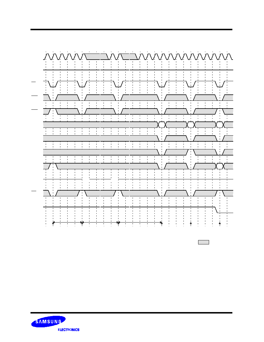
K5D5657DCM-F015
Revision 0.0
June 2003
- 57 -
MCP MEMORY
Preliminary
0
1
2
3
4
5
6
7
8
9
10
11
12
13
14
15
High level is necessary
CKE
CS
RAS
CAS
ADDR
BA0
BA1
DQ
A10/AP
WE
Power Up Sequence for Mobile SDRAM
DQM
Precharge
t
RP
16
17
18
19
20
21
22
24
23
25
Key
RAa
Hi-Z
Hi-Z
t
ARFC
t
ARFC
(All Bank)
Auto
Refresh
Auto
Refresh
Normal
MRS
Extended
MRS
Row Active
(A-Bank)
*NOTE:
1. Apply power and attempt to maintain CKE at a high state and all other inputs may be undefined.
- Apply V
DD
before or at the same time as V
DDQ
.
2. Maintain stable power, stable clock and NOP input condition for a minimum of 200us.
3. Issue precharge commands for all banks of the devices.
4. Issue 2 or more auto-refresh commands.
5. Issue a mode register set command to initialize the mode register.
6. Issue a extended mode register set command to define DS or PASR operating type of the device after normal MRS.
EMRS cycle is not mandatory and the EMRS command needs to be issued only when DS or PASR is used.
The default state without EMRS command issued is half driver strength, all 4 banks refreshed.
The device is now ready for the operation selected by EMRS.
For operating with DS or PASR, set DS or PASR mode in EMRS setting stage.
In order to adjust another mode in the state of DS or PASR mode, additional EMRS set is required but power up sequence is not needed again
at this time. In that case, all banks have to be in idle state prior to adjusting EMRS set.
: Don't care
Key
CLOCK
Hi
RAa
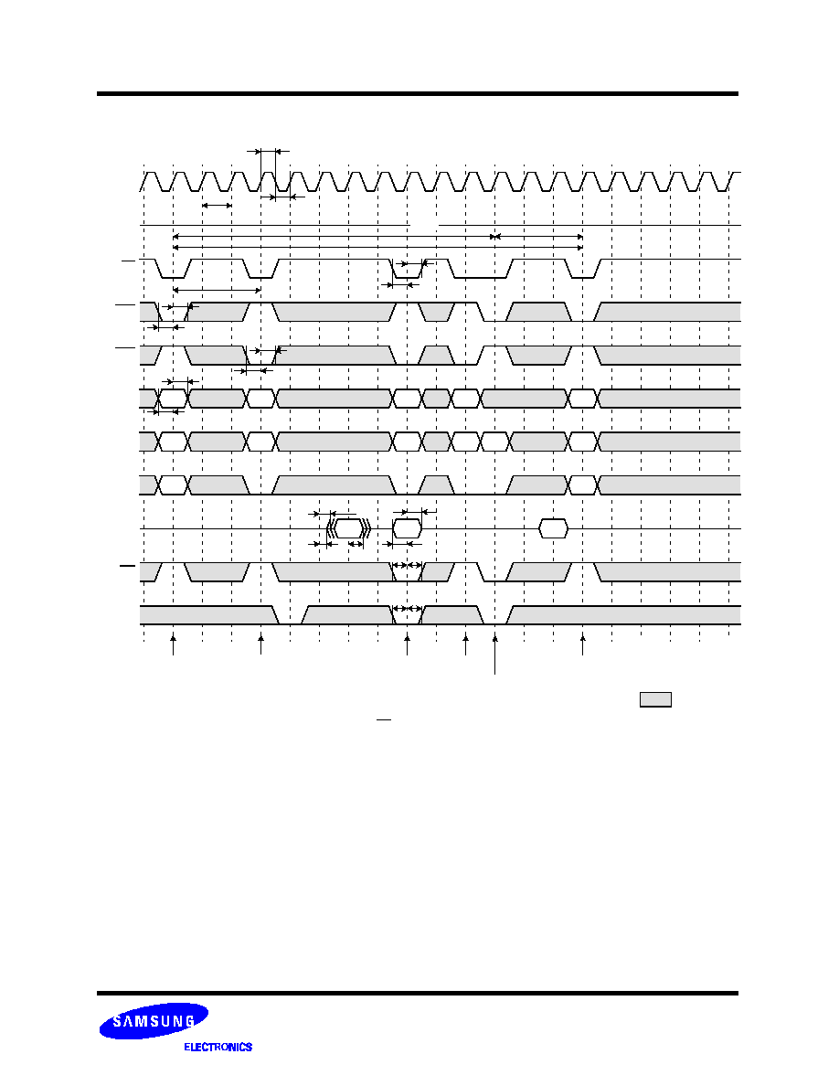
K5D5657DCM-F015
Revision 0.0
June 2003
- 58 -
MCP MEMORY
Preliminary
0
1
2
3
4
5
6
7
8
9
10
11
12
13
14
15
16
17
18
19
CKE
CS
RAS
CAS
BA0,BA1
A10/AP
WE
ADDR
DQM
: Don't care
CLOCK
Single Bit Read-Write-Read Cycle(Same Page) @CAS Latency=3, Burst Length=1
HIGH
Ra
Ca
BS
BS
Ra
DQ
Row Active
Read
Write
Read
Row Active
Precharge
t
CC
t
CH
t
CL
t
RAS
t
RC
t
SH
t
SS
*Note 1
t
RCD
t
RP
t
SH
t
SS
t
SH
t
SS
t
SH
t
SS
*Note 2
*Note 2,3
*Note 2,3
*Note 2,3 *Note 4
*Note 2
*Note 3
*Note 3
*Note 3
*Note 4
t
SS
t
SH
t
OH
t
SLZ
t
SAC
t
SH
t
SS
t
SH
t
SS
*NOTE:
1. All input except CKE & DQM can be don't care when CS is high at the CLK high going edge.
2. Bank active & read/write are controlled by BA0,BA1.
Cb
Cc
Rb
BS
BS
BS
BS
Qa
Db
Qc
Rb
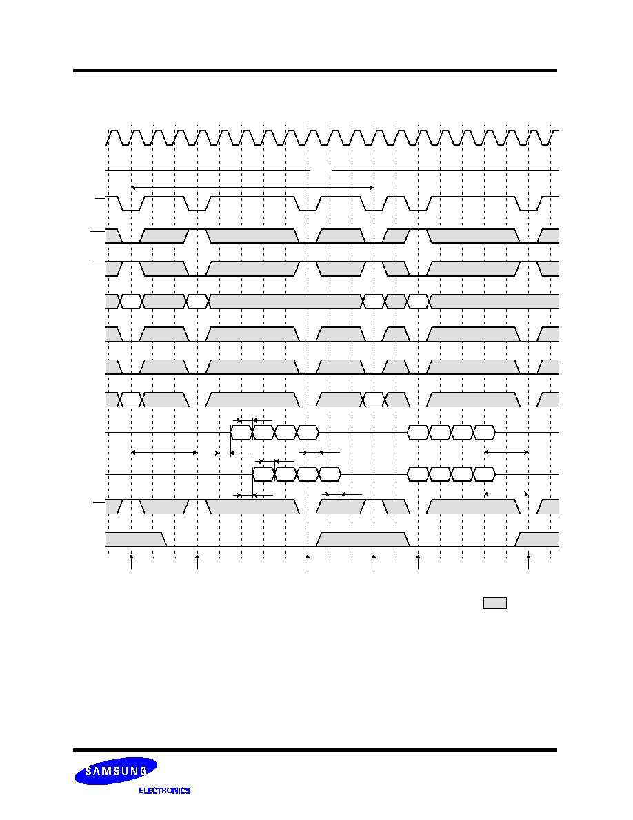
K5D5657DCM-F015
Revision 0.0
June 2003
- 59 -
MCP MEMORY
Preliminary
0
1
2
3
4
5
6
7
8
9
10
11
12
13
14
15
16
17
18
19
CKE
CS
RAS
CAS
BA1
A10/AP
CL=3
ADDR
WE
: Don't care
CLOCK
Read & Write Cycle at Same Bank @Burst Length=4, tRDL=2CLK
HIGH
Ra
Ca
Ra
CL=2
Row Active
Read
Write
Precharge
t
RC
*Note 1
t
SHZ
t
SAC
t
OH
*NOTE:
1. Minimum row cycle times is required to complete internal DRAM operation.
2. Row precharge can interrupt burst on any cycle. [CAS Latency - 1] number of valid output data
is available after Row precharge. Last valid output will be Hi-Z(t
SHZ
) after the clcok.
3. Ouput will be Hi-Z after the end of burst. (1, 2, 4, 8 & Full page bit burst)
BA0
DQM
DQ
t
RDL
*Note 2
*Note 4
t
SHZ
t
SAC
t
OH
t
RDL
*Note 4
(A-Bank)
(A-Bank)
(A-Bank)
(A-Bank)
Row Active
(A-Bank)
Precharge
(A-Bank)
{
t
RCD
Qa1
Db0
Qa0
Qa2
Db1
Db2
Db3
Qa3
Qa1
Db0
Qa0
Qa2
Db1
Db2
Db3
Qa3
Rb
Rb
Cb

K5D5657DCM-F015
Revision 0.0
June 2003
- 60 -
MCP MEMORY
Preliminary
0
1
2
3
4
5
6
7
8
9
10
11
12
13
14
15
16
17
18
19
CKE
CS
RAS
CAS
BA1
A10/AP
CL=3
ADDR
WE
: Don't care
CLOCK
Page Read & Write Cycle at Same Bank @Burst Length=4, tRDL=2CLK
HIGH
Ra
Ca
Ra
CL=2
Row Active
Read
Write
Precharge
*NOTE:
1. To write data before burst read ends, DQM should be asserted three cycle prior to write
command to avoid bus contention.
2. Row precharge will interrupt writing. Last data input, t
RDL
before Row precharge, will be written.
3. DQM should mask invalid input data on precharge command cycle when asserting precharge
before end of burst. Input data after Row precharge cycle will be masked internally.
4. t
DAL
,last data in to active delay, is 2CLK + t
RP
.
BA0
DQM
DQ
t
RDL
*Note 3
(A-Bank)
(A-Bank)
(A-Bank)
(A-Bank)
{
*Note 2
Cb
t
DAL
*Note 4
*Note 1
t
CDL
Read
(A-Bank)
Write
(A-Bank)
Row Active
(A-Bank)
Cc
Cd
Rb
Rb
Qa1
Dd0
Qa0
Qb0
Dd1
Qb1
Qb2
Dc0
Dc1
Qa1
Dd0
Qa0
Qb0
Dd1
Qb1
Dc0
Dc1
t
RCD

K5D5657DCM-F015
Revision 0.0
June 2003
- 61 -
MCP MEMORY
Preliminary
0
1
2
3
4
5
6
7
8
9
10
11
12
13
14
15
16
17
18
19
CKE
CS
RAS
CAS
BA1
A10/AP
CL=3
ADDR
WE
: Don't care
CLOCK
Page Read Cycle at Different Bank @Burst Length=4
HIGH
RAa
CAa
RAa
CL=2
Row Active
Read
Precharge
*NOTE:
1. CS can be don't cared when RAS, CAS and WE are high at the clock high going dege.
2. To interrupt a burst read by row precharge, both the read and the precharge banks must be the same.
BA0
DQM
DQ
(A-Bank)
(A-Bank)
(D-Bank)
{
*Note 2
RCc
Read
(B-Bank)
CBb
RDd
CCc
CDd
RBb
RCc
RDd
QAa1 QAa2 QBb0 QBb1 QBb2 QCc0 QCc1 QCc2 QDd0 QDd1 QDd2
QAa1 QAa2 QBb0 QBb1 QBb2 QCc0 QCc1 QCc2 QDd0 QDd1 QDd2
Row Active
(B-Bank)
Row Active
(C-Bank)
Row Active
(D-Bank)
Precharge
(A-Bank)
Read
(C-Bank)
Precharge
(B-Bank)
Read
(D-Bank)
Precharge
(C-Bank)
*Note 1
QAa0
QAa0
RBb
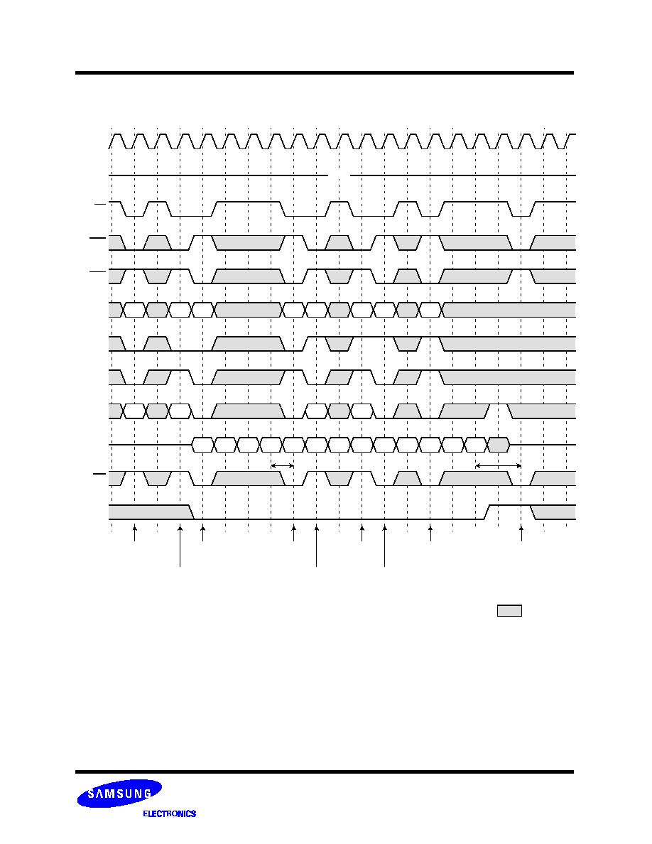
K5D5657DCM-F015
Revision 0.0
June 2003
- 62 -
MCP MEMORY
Preliminary
0
1
2
3
4
5
6
7
8
9
10
11
12
13
14
15
16
17
18
19
CKE
CS
RAS
CAS
BA1
A10/AP
ADDR
WE
: Don't care
CLOCK
Page Write Cycle at Different Bank @Burst Length=4, tRDL=2CLK
HIGH
RAa
Row Active
Write
Write
Precharge
*NOTE:
1. To interrupt burst write by Row precharge, DQM should be asserted to mask invalid input data.
2. To interrupt burst write by Row precharge, both the write and the precharge banks must be the same.
BA0
DQM
DQ
*Note 1
(A-Bank)
(A-Bank)
(D-Bank)
(All Banks)
*Note 2
RAb
CAa
CBb
RCc
RDd
CCc
RAa
RBb
RCc
RDd
DAa3 DBb0 DBb1 DBb2 DBb3 DCc0 DCc1 DDd0 DDd1 DDd2
t
CDL
t
RDL
Row Active
(B-Bank)
Write
(B-Bank)
Row Active
(C-Bank)
Row Active
(D-Bank)
Write
(C-Bank)
DAa2
DAa1
DAa0
CDd
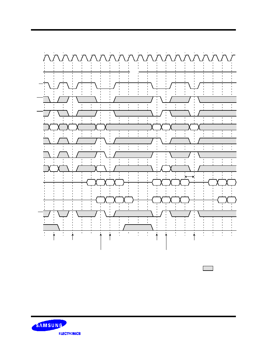
K5D5657DCM-F015
Revision 0.0
June 2003
- 63 -
MCP MEMORY
Preliminary
0
1
2
3
4
5
6
7
8
9
10
11
12
13
14
15
16
17
18
19
CKE
CS
RAS
CAS
BA1
A10/AP
CL=3
ADDR
WE
: Don't care
CLOCK
Read & Write Cycle at Different Bank @Burst Length=4
HIGH
RAa
RAa
CL=2
Row Active
Read
Write
Read
*NOTE:
1. t
CDL
should be met to complete write.
BA0
DQM
DQ
(A-Bank)
(A-Bank)
(D-Bank)
(B-Bank)
Precharge
(A-Bank)
{
CAa
RDb
RBc
CBc
RDb
t
CDL
*Note 1
Row Active
(D-Bank)
Row Active
(B-Bank)
QAa1
QAa0
QAa2 QAa3
QBc0 QBc1 QBc2
DDb0 DDb1 DDb2 DDb3
QAa1
QAa0
QAa2 QAa3
QBc0 QBc1
CDb
RBc
DDb0 DDb1 DDb2 DDb3
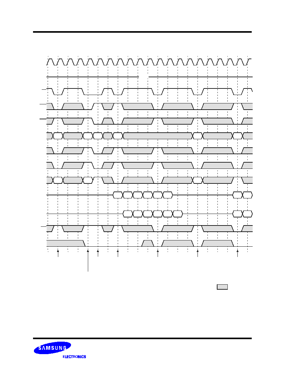
K5D5657DCM-F015
Revision 0.0
June 2003
- 64 -
MCP MEMORY
Preliminary
0
1
2
3
4
5
6
7
8
9
10
11
12
13
14
15
16
17
18
19
CKE
CS
RAS
CAS
BA1
A10/AP
CL=3
ADDR
WE
: Don't care
CLOCK
Read & Write Cycle with Auto Precharge I @Burst Length=4
HIGH
RAa
RAa
CL=2
Row Active
Read with
Precharge
Row Active
*NOTE:
1. When Read(Write) command with auto precharge is issued at A-Bank after A and B Bank activation.
- if Read(Write) command without auto precharge is issued at B-Bank before A-Bank auto precharge starts, A-Bank
auto precharge will start at B-Bank read command input point .
- any command can not be issued at A-Bank during t
RP
after A-Bank auto precharge starts.
BA0
DQM
DQ
(A-Bank)
Auto Pre
(B-Bank)
(A-Bank)
Read without Auto
Precharge(B-Bank)
RBb
RAc
CAc
CAa
CBb
RBb
DAc0
DAc0
charge
(A-Bank)
Row Active
(B-Bank)
Auto Precharge
Start Point
(A-Bank)
*Note1
Write with
Auto Precharge
(A-Bank)
QAa1
QAa0
QBb0 QBb1
DBb3
QBb2
QAa1
QAa0
QBb0 QBb1
DBb3
QBb2
DAc1
DAc1
RAc

K5D5657DCM-F015
Revision 0.0
June 2003
- 65 -
MCP MEMORY
Preliminary
0
1
2
3
4
5
6
7
8
9
10
11
12
13
14
15
16
17
18
19
CKE
CS
RAS
CAS
BA1
A10/AP
CL=3
ADDR
WE
: Don't care
CLOCK
Read & Write Cycle with Auto Precharge II @Burst Length=4
HIGH
Ra
CL=2
Row Active
Read with
*NOTE:
1. Any command to A-bank is not allowed in this period.
t
RP
is determined from at auto precharge start point
BA0
DQM
DQ
(A-Bank)
Auto Precharge
Auto Precharge
Start Point
Ca
Rb
(A-Bank)
(A-Bank)
Row Active
(B-Bank)
*Note1
Cb
Read with
Auto Precharge
(B-Bank)
Auto Precharge
Start Point
(B-Bank)
Rb
Qa1
Qa0
Qa2
Qa3
Qb1
Qb0
Qb2
Qb3
Qa1
Qa0
Qa2
Qa3
Qb1
Qb0
Qb2
Qb3
Ra
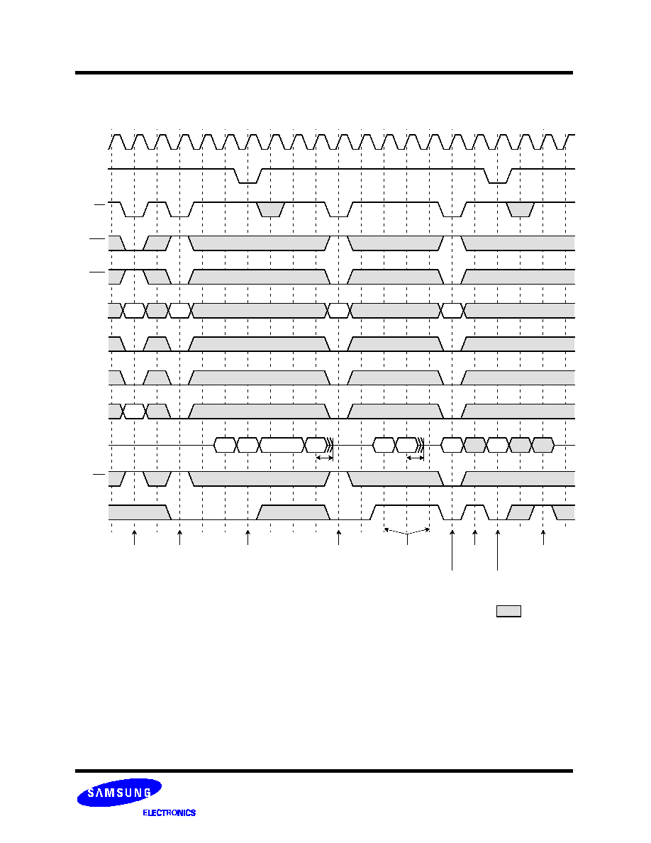
K5D5657DCM-F015
Revision 0.0
June 2003
- 66 -
MCP MEMORY
Preliminary
0
1
2
3
4
5
6
7
8
9
10
11
12
13
14
15
16
17
18
19
CKE
CS
RAS
CAS
BA1
A10/AP
ADDR
WE
: Don't care
CLOCK
Clock Suspension & DQM Operation Cycle @CAS Latency=2, Burst Length=4
Ra
Row Active
Read
Write
*NOTE:
1. DQM is needed to prevent bus contention.
BA0
DQM
DQ
*Note 1
DQM
Ca
Qb0
Qb1
Dc0
Dc2
Clock
Suspension
Write
Cb
Ra
t
SHZ
t
SHZ
Read
Clock
Suspension
Write
DQM
Read DQM
Qa1
Qa2
Qa3
Qa0
Cc

K5D5657DCM-F015
Revision 0.0
June 2003
- 67 -
MCP MEMORY
Preliminary
0
1
2
3
4
5
6
7
8
9
10
11
12
13
14
15
16
17
18
19
CKE
CS
RAS
CAS
BA1
A10/AP
CL=3
ADDR
WE
: Don't care
CLOCK
Read Interrupted by Precharge Command & Read Burst Stop Cycle @Full Page Burst
HIGH
RAa
CL=2
Row Active
*NOTE:
1. At full page mode, burst is finished by burst stop or precharge.
2. About the valid DQs after burst stop, it is same as the case of RAS interrupt.
Both cases are illustrated above timing diagram. See the label 1, 2 on them.
But at burst write, Burst stop and RAS interrupt should be compared carefully.
Refer the timing diagram of "Full page write burst stop cycle".
3. Burst stop is valid at every burst length.
BA0
DQM
QAa3
(A-Bank)
CAa
CAb
Burst Stop
Precharge
(A-Bank)
DQ
{
QAa4
1
1
QAa2 QAa3 QAa4
2
RAa
Read
(A-Bank)
Read
(A-Bank)
QAa1
QAa0
QAa2
QAa1
QAa0
QAb1
QAb0
QAb2 QAb3 QAb4 QAb5
QAb1
QAb0
QAb2 QAb3 QAb4 QAb5
2

K5D5657DCM-F015
Revision 0.0
June 2003
- 68 -
MCP MEMORY
Preliminary
0
1
2
3
4
5
6
7
8
9
10
11
12
13
14
15
16
17
18
19
CKE
CS
RAS
CAS
BA1
A10/AP
ADDR
WE
: Don't care
CLOCK
Write Interrupted by Precharge Command & Write Burst Stop Cycle @ Full Page Burst,
RAa
Row Active
Write
*NOTE:
1. At full page mode, burst is finished by burst stop or precharge.
2. Data-in at the cycle of interrupted by precharge can not be written into the corresponding
memory cell. It is defined by AC parameter of t
RDL
.
DQM at write interrupted by precharge command is needed to prevent invalid write.
DQM should mask invalid input data on precharge command cycle when asserting precharge
before end of burst. Input data after Row precharge cycle will be masked internally.
3. Burst stop is valid at every burst length.
BA0
DQM
DQ
CAa
CAb
Burst Stop
HIGH
RAa
DAa3 DAa4
DAb0 DAb1 DAb2 DAb3 DAb4 DAb5
t
BDL
*Note 1
t
RDL
*Note 1,2
(A-Bank)
(A-Bank)
Write
(A-Bank)
Precharge
(A-Bank)
tRDL=2CLK
DAa2
DAa1
DAa0

K5D5657DCM-F015
Revision 0.0
June 2003
- 69 -
MCP MEMORY
Preliminary
0
1
2
3
4
5
6
7
8
9
10
11
12
13
14
15
16
17
18
19
CKE
CS
RAS
CAS
BA1
A10/AP
CL=3
ADDR
WE
: Don't care
CLOCK
Burst Read Single bit Write Cycle @Burst Length=2
HIGH
RAa
CL=2
Row Active
*NOTE:
1. BRSW modes is enabled by setting A9 "High" at MRS (Mode Register Set).
At the BRSW Mode, the burst length at write is fixed to "1" regardless of programmed burst length.
2. When BRSW write command with auto precharge is executed, keep it in mind that t
RAS
should not be violated.
Auto precharge is executed at the burst-end cycle, so in the case of BRSW write command,
the next cycle starts the precharge.
BA0
DQM
(A-Bank)
CAa
RCc
Precharge
(C-Bank)
DQ
{
RAa
Write
(A-Bank)
*Note 2
RBb
CAb
CBc
CCd
RBb
RCc
Row Active
(B-Bank)
Read with
Auto Precharge
(A-Bank)
Row Active
(C-Bank)
Write with
Auto Precharge
(B-Bank)
Read
(C-Bank)
DAa0
QAb0 QAb1
DBc0
QCd0 QCd1
DAa0
QAb0 QAb1
DBc0
QCd0 QCd1

K5D5657DCM-F015
Revision 0.0
June 2003
- 70 -
MCP MEMORY
Preliminary
0
1
2
3
4
5
6
7
8
9
10
11
12
13
14
15
16
17
18
19
CKE
CS
RAS
CAS
A10/AP
ADDR
WE
: Don't care
CLOCK
Active/Precharge Power Down Mode @CAS Latency=2, Burst Length=4
Precharge
Row Active
Precharge
*NOTE:
1. All banks should be in idle state prior to entering precharge power down mode.
2. CKE should be set high at least 1CLK + t
SS
prior to Row active command.
3. Can not violate minimum refresh specification. (64ms)
BA
DQM
DQ
*Note 1
Power-down
*Note 2
Ra
Ca
Qa0
Qa1
Qa2
Precharge
Power-down
Read
Ra
t
SHZ
*Note 2
Entry
Exit
Active
Power-down
Entry
Active
Power-down
Exit
t
SS
*Note 3
t
SS
t
SS

K5D5657DCM-F015
Revision 0.0
June 2003
- 71 -
MCP MEMORY
Preliminary
0
1
2
3
4
5
6
7
8
9
10
11
12
13
14
15
16
17
18
19
CKE
CS
RAS
CAS
A10/AP
ADDR
WE
: Don't care
CLOCK
Self Refresh Entry & Exit Cycle
Self Refresh Entry
*NOTE:
TO ENTER SELF REFRESH MODE
1. CS, RAS & CAS with CKE should be low at the same clcok cycle.
2. After 1 clock cycle, all the inputs including the system clock can be don't care except for CKE.
3. The device remains in self refresh mode as long as CKE stays "Low".
cf.) Once the device enters self refresh mode, minimum t
RAS
is required before exit from self refresh.
TO EXIT SELF REFRESH MODE
4. System clock restart and be stable before returning CKE high.
5. CS starts from high.
6. Minimum t
RC
is required after CKE going high to complete self refresh exit.
7. 4K cycle(64Mb ,128Mb) or 8K cycle(256Mb, 512Mb) of burst auto refresh is required before self refresh entry and
after self refresh exit if the system uses burst refresh.
BA0,BA1
DQM
DQ
*Note 1
*Note 4
t
SS
*Note 3
t
SRFX
*Note 2
*Note 6
Self Refresh Exit
Auto Refresh
Hi-Z
Hi-Z
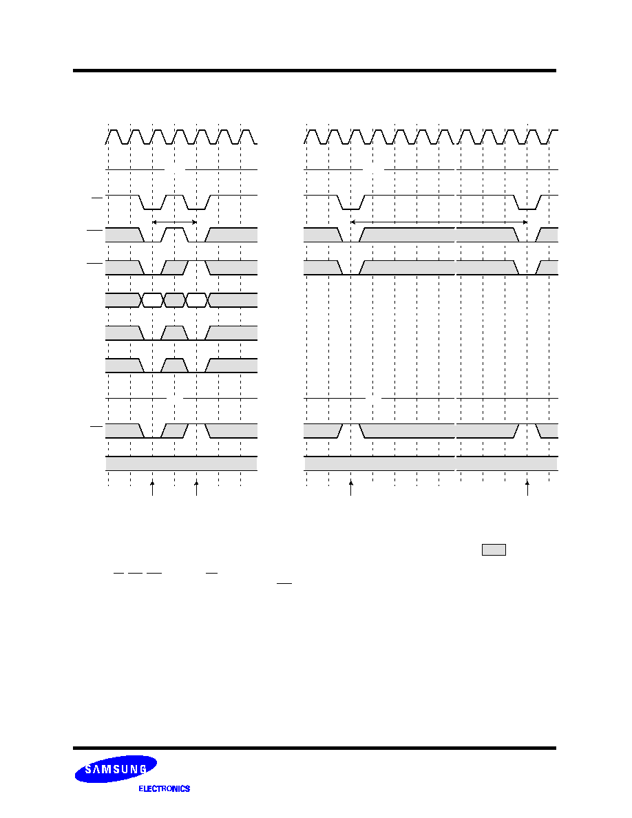
K5D5657DCM-F015
Revision 0.0
June 2003
- 72 -
MCP MEMORY
Preliminary
0
1
2
3
4
5
6
0
10
CKE
CS
RAS
CAS
BA1
ADDR
WE
: Don't care
CLOCK
Mode Register Set Cycle
Key
MRS
New Command
*NOTE:
MODE REGISTER SET CYCLE
1. CS, RAS, CAS, BA0, BA1 & WE activation at the same clock cycle with address key will set internal mode register.
2. Minimum 2 clock cycles should be met before new RAS activation.
3. Please refer to Mode Register Set table.
BA0
DQM
DQ
Ra
Auto Refresh
Auto Refresh Cycle
1
2
3
4
5
6
7
8
9
HIGH
HIGH
New Command
* All banks precharge should be completed before Mode Register Set cycle and auto refresh cycle.
*Note 2
*Note 1
*Note 3
t
ARFC
Hi-Z
Hi-Z
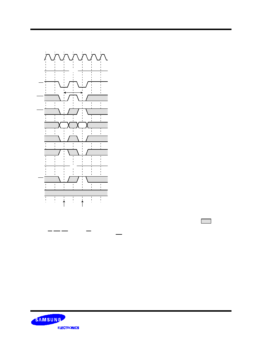
K5D5657DCM-F015
Revision 0.0
June 2003
- 73 -
MCP MEMORY
Preliminary
0
1
2
3
4
5
6
CKE
CS
RAS
CAS
BA1
ADDR
WE
: Don't care
CLOCK
Extended Mode Register Set Cycle
Key
EMRS
New Command
*NOTE:
EXTENDED MODE REGISTER SET CYCLE
1. CS, RAS, CAS, BA0, BA1 & WE activation at the same clock cycle with address key will set internal mode register.
2. Minimum 2 clock cycles should be met before new RAS activation.
3. Please refer to Mode Register Set table.
BA0
DQM
DQ
Ra
HIGH
*Note 2
*Note 1
*Note 3
Hi-Z

K5D5657DCM-F015
Revision 0.0
June 2003
- 74 -
MCP MEMORY
Preliminary
PACKAGE DIMENSION
107-Ball Fine pitch Ball Grid Array Package (measured in millimeters)
Units:millimeters
0.10 MAX
0
.
4
5
±
0
.
0
5
0.32
±
0.05
1.30
±
0.10
TOP VIEW
10.50
±
0.10
1
3
.
0
0
±
0
.
1
0
#A1
1
3
.
0
0
±
0
.
1
0
107-
0.45
±
0.05
0
.
8
0
0.20
M
A B
(Datum A)
1
4
2
7
6
5
3
8
#A1 INDEX MARK
10.50
±
0.10
1
3
.
0
0
±
0
.
1
0
0.80
9
10
0.80x9=7.20
0
.
8
0
x
1
3
=
1
0
.
4
0
A
B
C
E
G
D
F
H
J
L
K
M
N
P
(Datum B)
5
.
2
0
3.60
A
B
BOTTOM VIEW