K5Q6432YCM - T010
Revision 0.3
June. 2001
- 1 -
Document Title
Multi-Chip Package MEMORY
64M Bit (8Mx8) Nand Flash Memory / 32M Bit
(2Mx16) UtRAM
Revision History
The attached datasheets are prepared and approved by SAMSUNG Electronics. SAMSUNG Electronics CO., LTD. reserve the right
to change the specifications. SAMSUNG Electronics will evaluate and reply to your requests and questions about device. If you have
any questions, please contact the SAMSUNG branch office near you.
Revision No.
0.0
0.1
0.2
0.3
Remark
Advanced
Information
Preliminary
Preliminary
Final
History
Initial issue.
Changed Device name
K5Q6420YCM-TO70 -> K5Q6432YCM-T010
<UtRAM>
- Improve operating current from 30mA to 25mA..
- Release speed from 70ns to 100ns.
- Release standby current form 170
�
A to 200
�
A.
- Add Power up timing diagram.
- Add AC characteristics for continuous write.
- Expand max operating temperature from 70
�
C to 85
�
C.
- Changed I
OL
/ I
OH
from 1.0mA/-0.5mA to 0.1mA/-0.1mA.
<UtRAM>
- Release standby current from 200uA to 250uA
- Release deep power down current from 10uA to 20uA
- Release tWC for continuous write operation from 100ns to 110ns
- Release tCW for continuous write operation from 90ns to 100ns
- Release tAW for continuous write operation from 90ns to 100ns
- Release tBW for continuous write operation from 90ns to 100ns
- Release tWP for continuous write operation from 90ns to 100ns
<UtRAM>
- Improve standby current from 250uA to 150uA
Draft Date
Dec. 19th 2000
Feb. 28th 2001
April. 6th 2001
June. 11th 2001
Note : For more detailed features and specifications including FAQ, please refer to Samsung's web site.
http://samsungelectronics.com/semiconductors/products/products_index.html
K5Q6432YCM - T010
Revision 0.3
June. 2001
- 2 -
Multi-Chip Package MEMORY
64M Bit (8Mx8) Nand Flash Memory / 32M Bit
(2Mx16) UtRAM
The K5Q6432YCM
featuring single 3.0V power supply is a Multi
Chip Package Memory which combines 64Mbit Nand Flash and
32Mbit Unit Transistor CMOS RAM.
The 64Mbit Flash memory is organized as 8M x8 bit and the
32Mbit UtRAM is organized as 2M x16 bit. In 64Mb NAND Flash
a 528-byte page program can be typically achieved within 300us
and an 8K-byte block erase can be typically achieved within 2ms.
In serial read operation, a byte can be read by 50ns. The DQ pins
serve as the ports for address and data input/output as well as
command inputs. Even the write-intensive systems can take
advantage of the FLASH
s extended reliability of 100K program/
erase cycles by providing ECC(Error Correcting Code) with real
time mapping-out algorithm. These algorithms have been imple-
mented in many mass storage applications and also the spare 16
bytes of a page combined with the other 512 bytes can be utilized
by system-level ECC. The K5Q6432YCM is suitable for use in
data memory of mobile communication system to reduce not only
mount area but also power consumption. This device is available
in 69-ball TBGA Type.
FEATURES
�
Power Supply voltage : 2.7V to 3.3 V
�
Organization
- Flash : (8M + 256K)bit x 8bit
- UtRAM : 2M x 16 bit
�
Access Time
- Flash : Random access : 10us(Max.), Serial read : 50ns(Min.)
- UtRAM :
100 ns
�
Power Consumption (typical value)
- Flash Read Current : 10 mA(@20MHz)
Program/Erase Current : 10 mA
Standby Current : 10
�
A
- UtRAM Operating Current : 18 mA
Standby Current : 120
�
A
�
Flash Automatic Program and Erase
Page Program : (512 + 16)Byte
Block Erase : (8K + 256)Byte
�
Flash Fast Write Cycle Time
Program time : 300us(Typ.)
Block Erase Time : 2ms(Typ.)
�
Flash Endurance : 100,000 Program/Erase Cycles Minimum
�
Flash Data Retention : 10 years
�
Operating Temperature : -25
�
C ~ 85
�
C
�
Package : 69 - ball TBGA Type - 8 x 13mm, 0.8 mm pitch
GENERAL DESCRIPTION
SAMSUNG ELECTRONICS CO., LTD. reserves the right to change products and specifications without notice.
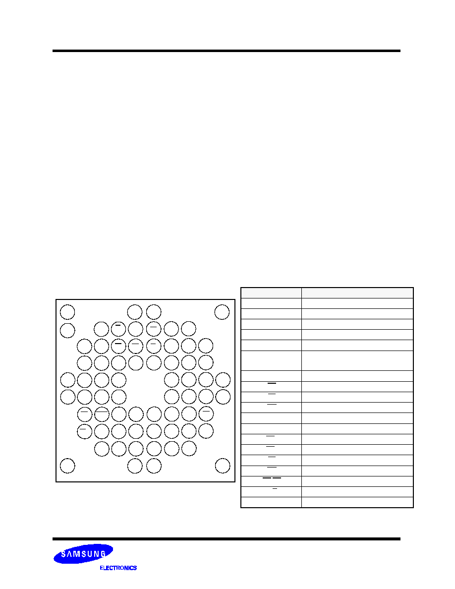
BALL CONFIGURATION
Ball Name
Description
A
0
to A
20
Address Input Balls (UtRAM)
DQ
0
to DQ
7
Data Input/Output Balls (Common)
DQ
8
to DQ
15
Data Input/Output Balls (UtRAM)
Vccu
Power Supply (UtRAM)
Vcc
F
Power Supply (Flash Memory)
VccQ
F
Output Buffer Power (Flash Memory)
This input may be tied directly to V
CCF
.
Vss
Ground (Common)
UB
Upper Byte Enable (UtRAM)
LB
Lower Byte Enable (UtRAM)
WP
Write Protection (Flash Memory)
CLE
Command Latch Enable(Flash Memory)
ALE
Address Latch Enable(Flash Memory)
CE
F
Chip Enable (Flash Memory)
CS
U
Chip Enable (UtRAM Low Active)
ZZ
Deep Power Down(UtRAM High Active)
WE
Write Enable (Common)
OE/RE
Output Enable (Common)
R/B
Ready/Busy (Flash memory)
N.C
No Connection
A7
UB
A8
A3
A6
CEf
LB
ZZ
A19
A2
A5
A18
ALE
A20
A9
A4
DQ6
WP
OE/RE
DQ9
DQ3
DQ4
DQ13
1
2
3
4
5
6
A
B
C
D
E
F
CLE
WE
V
SS
A10
DQ1
A0
A1
A17
A11
A12
A15
A13
N.C
A14
N.C
A16
R/B
7
8
Vccf
DQ8
DQ2
DQ11
DQ5
H
DQ14
CSu
DQ0
DQ10
VccQ
F
Vcc
U
DQ12
G
DQ7
Vss
N.C
DQ15
N.C
N.C
N.C
N.C
N.C
N.C
N.C
N.C
N.C
N.C
N.C
N.C
Index
9
10
K
J
BALL DESCRIPTION
69 Ball TBGA , 0.8mm Pitch
Top View (Ball Down)
K5Q6432YCM - T010
Revision 0.3
June. 2001
- 4 -
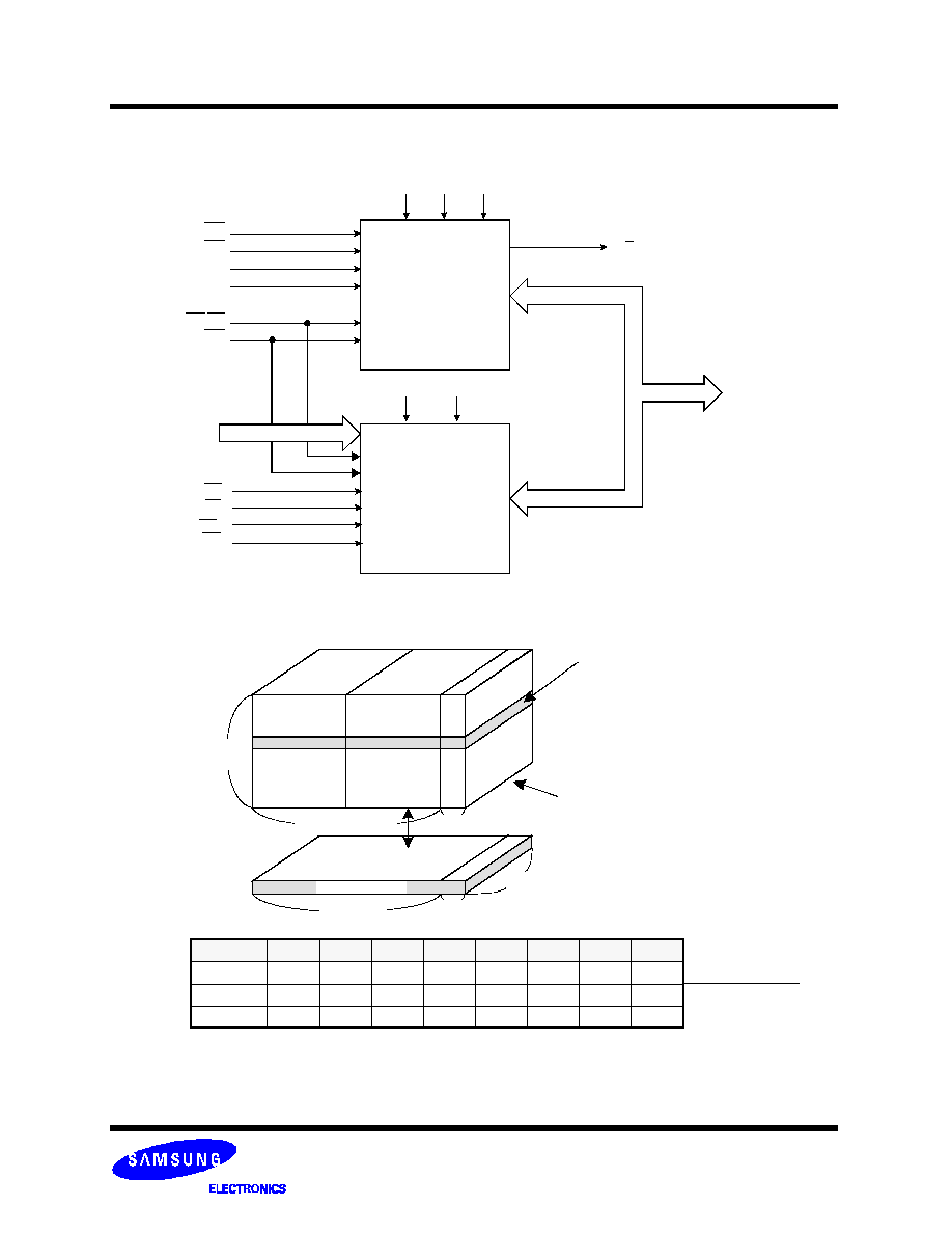
NAND FLASH PRODUCT INTRODUCTION
The Flash Memory is a 69Mbit(69,206,016 bit) memory organized as 16,384 rows(pages) by 528 columns. Spare sixteen columns
are located from column address of 512 to 527. A 528-byte data register is connected to memory cell arrays accommodating data
transfer between the DQ buffers and memory during page read and page program operations. The memory array is made up of 16
cells that are serially connected to form a NAND structure. Each of the 16 cells resides in a different page. A block consists of the 16
pages formed by one NAND structures, totaling 4,224 NAND structures of 16 cells. The array organization is shown in Figure 2. The
program and read operations are executed on a page basis, while the erase operation is executed on a block basis. The memory
array consists of 1024 separately erasable 8K-byte blocks. It indicates that the bit by bit erase operation is prohibited on the Flash
Memory.
The Flash Memory has addresses multiplexed into 8 DQ
s. This scheme dramatically reduces pin counts and allows systems
upgrades to future densities by maintaining consistency in system board design. Command, address and data are all written through
DQ
s by bringing WE to low while CE is low. Data is latched on the rising edge of WE. Command Latch Enable(CLE) and Address
Latch Enable(ALE) are used to multiplex command and address respectively, via the DQ pins. All commands require one bus cycle
except for Block Erase command which requires two cycles: one cycle for erase-setup and another for erase-execution after block
address loading. The 8M byte physical space requires 23 addresses, thereby requiring three cycles for byte-level addressing: col-
umn address, low row address and high row address, in that order. Page Read and Page Program need the same three address
cycles following the required command input. In Block Erase operation, however, only the two row address cycles are used.
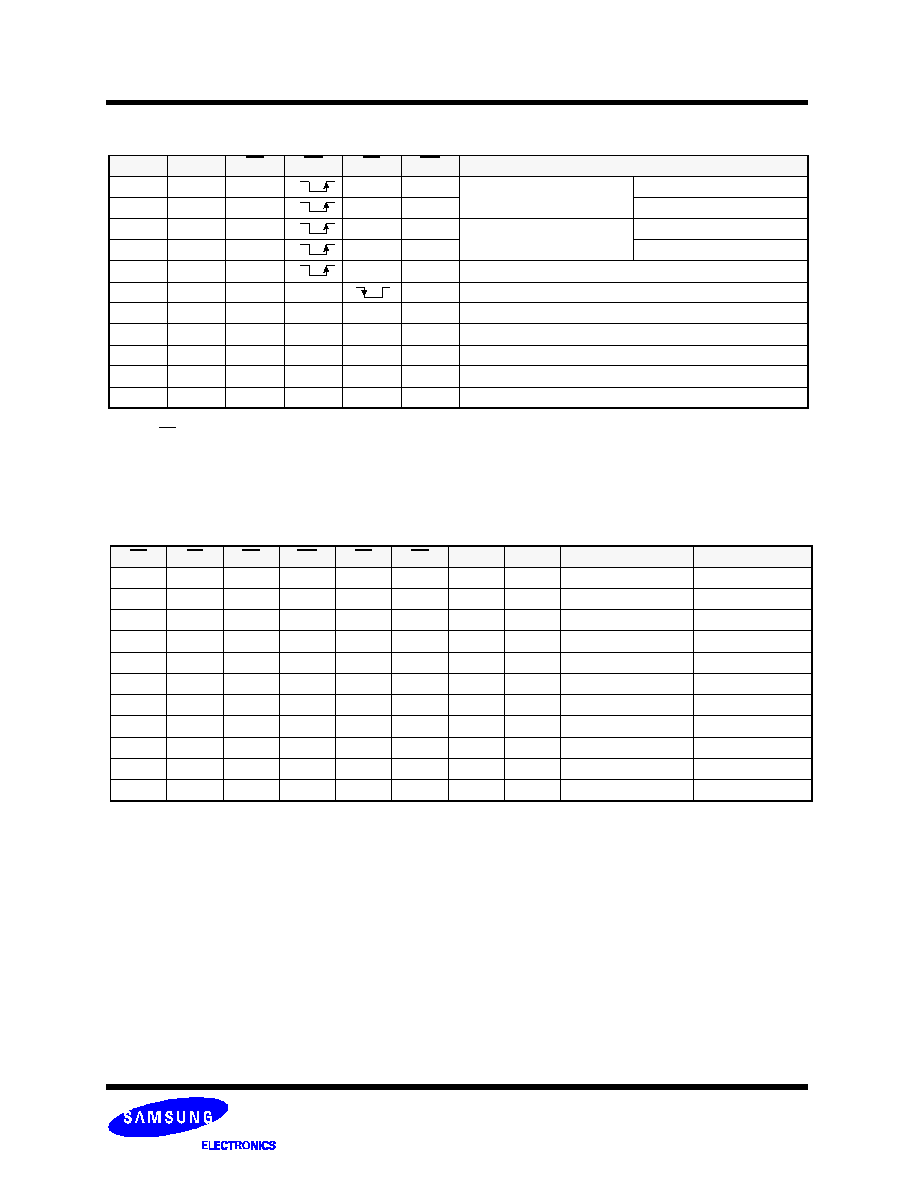
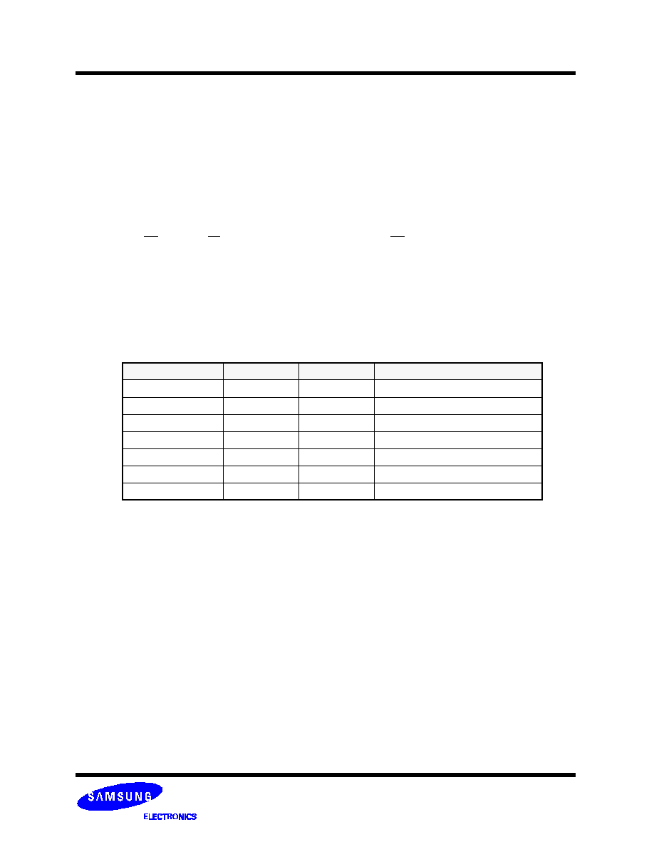
Device operations are selected by writing specific commands into the command register. Table 1 defines the specific commands of
the Flash Memory.
Table 1. COMMAND SETS
NOTE : 1. The 00h command defines starting address of the 1st half of registers.
The 01h command defines starting address of the 2nd half of registers.
After data access on the 2nd half of register by the 01h command, the status pointer is
automatically moved to the 1st half register(00h) on the next cycle.
Function
1st. Cycle
2nd. Cycle
Acceptable Command during Busy
Read 1
00h/01h
(1)
-
Read 2
50h
-
Read ID
90h
-
Reset
FFh
-
O
Page Program
80h
10h
Block Erase
60h
D0h
Read Status
70h
-
O