Revision 3.0
CMOS SRAM
K6F1016V3M, K6F1016S3M, K6F1016R3M Family
1
May 1999
Document Title
64K x16 bit Super Low Power and Low Voltage Full CMOS Static RAM
Revision History
Revision No.
0.0
0.1
1.0
2.0
3.0
Remark
Advance
Preliminary
Final
Final
Final
History
Initial draft
Revise
- Erase 100ns part from KM616FS1000 Family
- Add 150ns part on KM616FS1000 Family
- Add 32-sTSOP1 new package
- Add high power version
I
SB1
=5.0
µ
A(Max)
- Change V
DR
(Min) 1.0 to 1.5V
Finalize
- Concept change high power version to low low power version
I
SB1
=5
.0µ
A(Max)
- Change super low power version with special handling
I
SB1
=1.0
µ
A(Max)
- Reduce Icc & Icc1
Read : 15mA to 10mA
Write : 25mA to 20mA
Revise
- Change datasheet format
- Erase reverse type package
Revise
- Add 48-
µ
BGA type package
Draft Date
March 15, 1996
June 3, 1996
December 1, 1996
February 26, 1998
May 3, 1999
The attached datasheets are provided by SAMSUNG Electronics. SAMSUNG Electronics CO., LTD. reserve the right to change the specifications and
products. SAMSUNG Electronics will answer to your questions about device. If you have any questions, please contact the SAMSUNG branch offices.
Revision 3.0
CMOS SRAM
K6F1016V3M, K6F1016S3M, K6F1016R3M Family
2
May 1999
64Kx16 bit Super Low Power and Low Voltage Full CMOS Static RAM
GENERAL DESCRIPTION
The K6F1016V3M, K6F1016S3M and K6F1016R3M fami-
lies are fabricated by SAMSUNG
s advanced Full CMOS
process technology. The families support various operating
temperature ranges for user flexibility of system design. The
families also support low data retention voltage for battery
back-up operation with low data retention current.
FEATURES
∑
Process Technology: Full CMOS
∑
Organization: 64Kx16 bit
∑
Power Supply Voltage
K6F1016V3M Family: 3.0V~3.6V
K6F1016S3M Family: 2.3V~3.3V
K6F1016R3M Family: 1.8V~2.7V
∑
Low Data Retention Voltage: 1.5V(Min)
∑
Three state output status and TTL Compatible
∑
Package Type: 44-TSOP2-400F, 48-
µ
BGA-6.00x8.00
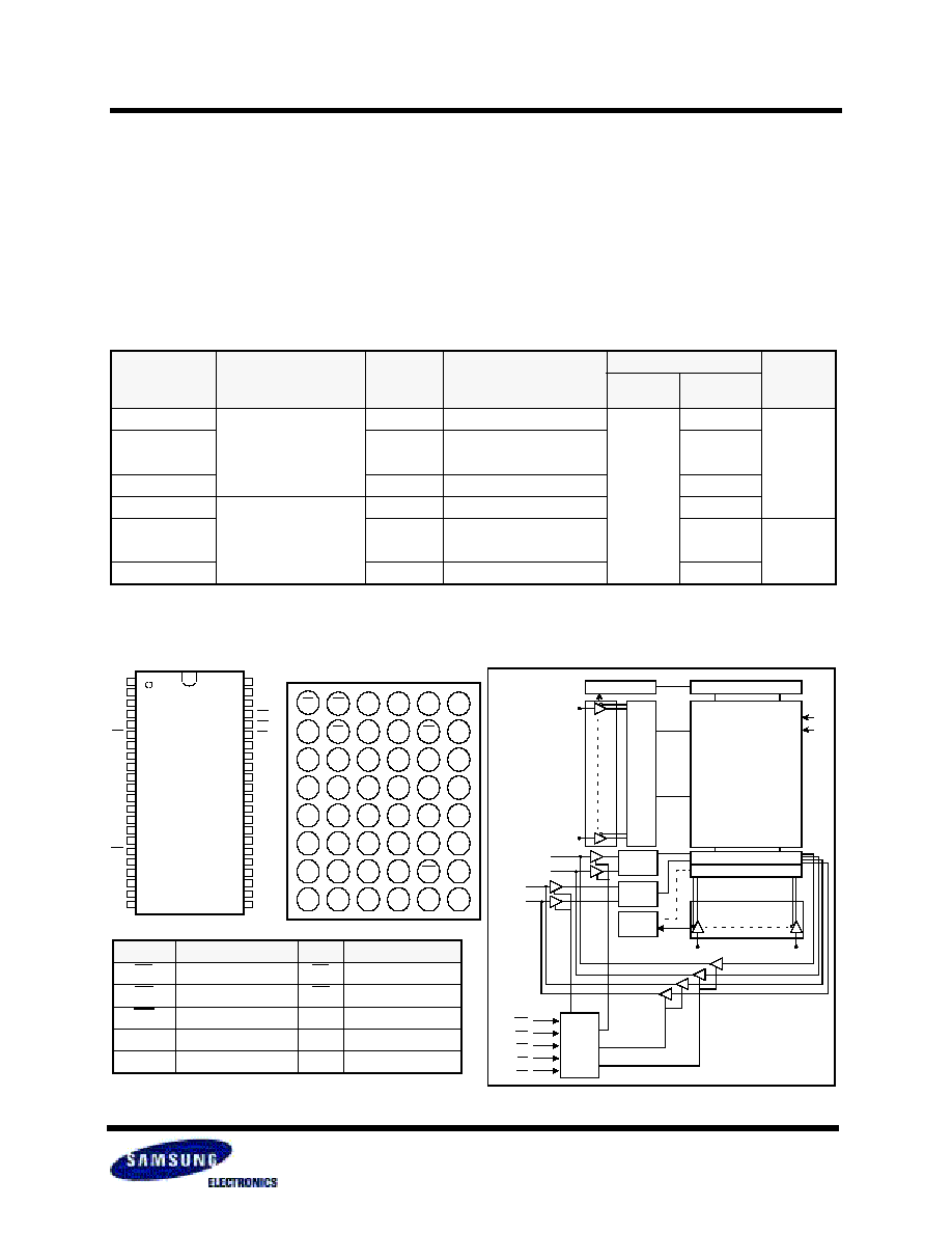
PIN DESCRIPTION
Name
Function
Name
Function
CS
Chip Select Input
LB
Lower Byte(I/O
1
~
8
)
OE
Output Enable Input
UB
Upper Byte(I/O
9
~
16
)
WE
Write Enable Input
Vcc
Power
A
0
~A
15
Address Inputs
Vss
Ground
I/O
1
~I/O
16
Data Inputs/Outputs
N.C. No Connection
PRODUCT FAMILY
1. The parameter is measured with 30pF test load.
2. Super low power product=1
µ
A with special handling.
3. Availiable parts are 100ns@V
CC
=3.0
±
0.3V, 150ns@V
CC
=2.5
±
0.2V and 300ns@V
CC
=2.0
±
0.2V with 30pF test load.
Product Family
Operating Temperature
Vcc Range
Speed(ns)
Power Dissipation
PKG Type
Standby
(I
SB1
, Max)
Operating
(I
CC2
, Max)
K6F1016V3M-C
Commercial(0~70
∞
C)
3.0~3.6V
70
1)
/85@V
CC
=3.3
±
0.3V
5
µ
A
2)
80mA
44-TSOP2
Forward
K6F1016S3M-C
2.3~3.3V
70
1)
/85@V
CC
=3.0
±
0.3V
80mA
120
1)
/150@V
CC
=2.5
±
0.2V
50mA
K6F1016R3M-C
1.8~2.7V
300
1)
@V
CC
=2.0
±
0.2V
20mA
K6F1016V3M-I
Industrial(-40~85
∞
C)
3.0~3.6V
70
1)
/85@V
CC
=3.3
±
0.3V
80mA
K6F1016S3M-I
2.3~3.3V
70
1)
/85@V
CC
=3.0
±
0.3V
80mA
44-TSOP2
Forward
48-
µ
BGA
3)
120
1)
/150@V
CC
=2.5
±
0.2V
50mA
K6F1016R3M-I
1.8~2.7V
300
1)
@V
CC
=2.0
±
0.2V
20mA
FUNCTIONAL BLOCK DIAGRAM
A4
A3
A2
A1
A0
CS
I/OI
I/O2
I/O3
I/O4
Vcc
Vss
I/O5
I/O6
I/O7
I/O8
WE
A15
A14
A13
A12
N.C
A5
A6
A7
OE
UB
LB
I/O16
I/O15
I/O14
I/O13
Vss
Vcc
I/O12
I/O11
I/O10
I/O9
N.C
A8
A9
A10
A11
N.C
44-TSOP2
Forward
44
43
42
41
40
39
38
37
36
35
34
33
32
31
30
29
28
27
26
25
24
23
1
2
3
4
5
6
7
8
9
10
11
12
13
14
15
16
17
18
19
20
21
22
SAMSUNG ELECTRONICS CO., LTD. reserves the right to change products and specifications without notice.
Precharge circuit.
Memory array
1024 rows
64
◊
16 columns
I/O Circuit
Column select
Clk gen.
Row
select
A10
A13
A12
A11 A9
A8
A7
A6
A5
A4
A3
A2
A1
A0
WE
OE
UB
CS
I/O
1
~I/O
8
A15
Data
cont
Data
cont
Data
cont
LB
I/O
9
~I/O
16
Vcc
Vss
A14
Control
logic
LB
OE
A0
A1
A2
N.C
I/O9
UB
A3
A4
CS
I/O1
I/O10
I/O11
A5
A6
I/O2
I/O3
Vss
I/O12
N.C
A7
I/O4
Vcc
Vcc
I/O13
N.C
N.C
I/O5
Vss
I/O15
I/O14
A14
A15
I/O6
I/O7
I/O16
N.C
A12
A13
WE
I/O8
N.C
A8
A9
A10
A11
N.C
1
2
3
4
5
6
A
B
C
D
E
F
G
H
48-
µ
BGA Top View
Revision 3.0
CMOS SRAM
K6F1016V3M, K6F1016S3M, K6F1016R3M Family
3
May 1999
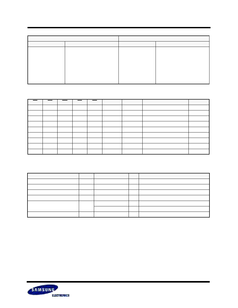
ABSOLUTE MAXIMUM RATINGS
1)
1. Stresses greater than those listed under "Absolute Maximum Ratings" may cause permanent damage to the device. Functional operation should be
restricted to recommended operating condition. Exposure to absolute maximum rating conditions for extended periods may affect reliability.
2. V
IN
/V
OUT
=-0.2 to 3.9V for K6F1016V3M Family.
3. V
CC
=-0.2 to 4.6V for K6F1016V3M Family.
Item
Symbol
Ratings
Unit
Remark
Voltage on any pin relative to Vss
V
IN
,V
OUT
-0.2 to 3.6V
2)
V
-
Voltage on Vcc supply relative to Vss
V
CC
-0.2 to 4.0V
3)
V
-
Power Dissipation
P
D
1.0
W
-
Storage temperature
T
STG
-55 to 150
∞
C
-
Operating Temperature
T
A
0 to 70
∞
C
K6F1016V3M-C
,
K6F1016S3M-C
,
K6F1016R3M-C
-40 to 85
∞
C
K6F1016V3M-
I,
K6F1016S3M-
I,
K6F1016R3M-
I
Soldering temperature and time
T
SOLDER
260
∞
C, 5sec(Lead Only)
-
-
PRODUCT LIST
Commercial Temperature Products(0~70
∞
C)
Industrial Temperature Products(-40~85
∞
C)
Part Name
Function
Part Name
Function
K6F1016V3M-TB70
K6F1016V3M-TB85
K6F1016S3M-TB12
K6F1016S3M-TB15
K6F1016R3M-TB30
44-TSOP2 F, 70ns, 3.3V, LL
44-TSOP2 F, 85ns, 3.3V, LL
44-TSOP2 F, 120/70ns, 2.5/3.0V, LL
44-TSOP2 F, 150/85ns, 2.5/3.0V, LL
44-TSOP2 F, 300ns, 2.0/2.5V, LL
K6F1016V3M-TF70
K6F1016V3M-TF85
K6F1016S3M-TF12
K6F1016S3M-TF15
K6F1016S3M-ZF15
K6F1016R3M-TF30
K6F1016R3M-ZF30
44-TSOP2 F, 70ns, 3.3V, LL
44-TSOP2 F, 85ns, 3.3V, LL
44-TSOP2 F, 120/70ns, 2.5/3.0V, LL
44-TSOP2 F, 150/85ns, 2.5/3.0V, LL
48-
µ
BGA, 2.5V/3.0V, 150/100ns
44-TSOP2 F, 300ns, 2.0/2.5V, LL
48-
µ
BGA, 1.8V/2.5V, 300ns
FUNCTIONAL DESCRIPTION
1. X means don
t care. (Must be in low or high state)
CS
OE
WE
LB
UB
I/O
1~8
I/O
9~16
Mode
Power
H
X
1)
X
1)
X
1)
X
1)
High-Z
High-Z
Deselected
Standby
L
H
H
X
1)
X
1)
High-Z
High-Z
Output Disabled
Active
L
X
1)
X
1)
H
H
High-Z
High-Z
Output Disabled
Active
L
L
H
L
H
Dout
High-Z
Lower Byte Read
Active
L
L
H
H
L
High-Z
Dout
Upper Byte Read
Active
L
L
H
L
L
Dout
Dout
Word Read
Active
L
X
1)
L
L
H
Din
High-Z
Lower Byte Write
Active
L
X
1)
L
H
L
High-Z
Din
Upper Byte Write
Active
L
X
1)
L
L
L
Din
Din
Word Write
Active
Revision 3.0
CMOS SRAM
K6F1016V3M, K6F1016S3M, K6F1016R3M Family
4
May 1999
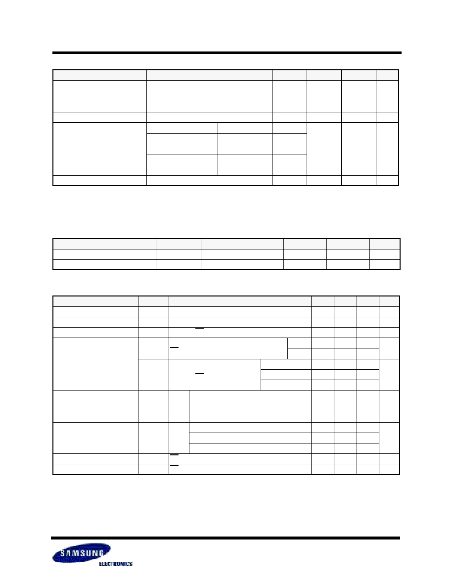
RECOMMENDED DC OPERATING CONDITIONS
1)
Note
1 Commercial Product : T
A
=0 to 70
∞
C, unless otherwise specified
Industrial Product : T
A
=-40 to 85
∞
C, unless otherwise specified
2. Overshoot : Vcc + 1.0V in case of pulse width
20ns
3. Undershoot : -1.0V in case of pulse width
20ns
4. Overshoot and undershoot are sampled, not 100% tested.
Item
Symbol
Product
Min
Typ
Max
Unit
Supply voltage
Vcc
K6F1016V3M Family
3.0
3.3
3.6
V
K6F1016S3M Family
2.3
2.5/3.0
3.3
K6F1016R3M Family
1.8
2.0/2.5
2.7
Ground
Vss
All Family
0
0
0
V
Input high voltage
V
IH
K6F1016V3M Family
Vcc=3.3
±
0.3V
2.2
-
Vcc+0.2
2)
V
K6F1016S3M Family
Vcc=3.0
±
0.3V
2.2
Vcc=2.5
±
0.2V
2.0
K6F1016R3M Family
Vcc=2.5
±
0.2V
2.0
Vcc=2.0
±
0.2V
1.6
Input low voltage
V
IL
All Family
-0.2
3)
-
0.4
V
CAPACITANCE
1)
(f=1MHz, T
A
=25
∞
C)
1. Capacitance is sampled, not 100% tested
Item
Symbol
Test Condition
Min
Max
Unit
Input capacitance
C
IN
V
IN
=0V
-
8
pF
Input/Output capacitance
C
IO
V
IO
=0V
-
10
pF
DC AND OPERATING CHARACTERISTICS
1. Super low power product=1
µ
A with special handling.
Item
Symbol
Test Conditions
Min
Typ
Max
Unit
Input leakage current
I
LI
V
IN
=Vss to Vcc
-1
-
1
µ
A
Output leakage current
I
LO
CS=V
IH
or OE=V
IH
or WE=V
IL
, V
IO
=Vss to Vcc
-1
-
1
µ
A
Operating power supply current
I
CC
I
IO
=0mA, CS=V
IL
, V
IN
=V
IL
or V
IH
, Read
-
-
2
mA
Average operating current
I
CC1
Cycle time=1
µ
s, 100% duty, I
IO
=0mA,
CS
0.2V, V
IN
0.2V or V
IN
V
CC
-0.2V
Read
-
-
5
mA
Write
-
-
20
I
CC2
Cycle time=Min, 100% duty,
I
IO
=0mA, CS=V
IL
, V
IN
=V
IL
or V
IH
Vcc=3.3V@70ns
-
-
65
mA
Vcc=2.7V@120ns
-
-
55
Vcc=2.2V@300ns
-
-
20
Output low voltage
V
OL
I
OL
2.1mA at Vcc=3.0/3.3V
-
-
0.4
V
0.5mA at Vcc=2.5V
0.33mA at Vcc=2.0V
Output high voltage
V
OH
I
OH
-1.0mA at Vcc=3.0/3.3V
2.4
-
-
V
-0.5mA at Vcc=2.5V
2.0
-
-
-0.44mA at Vcc=2.0V
1.6
-
-
Standby Current(TTL)
I
SB
CS=V
IH
, Other inputs=V
IL
or V
IH
-
-
0.3
mA
Standby Current(CMOS)
I
SB1
CS
Vcc-0.2V, Other inputs=0~Vcc
-
-
5
1)
µ
A
Revision 3.0
CMOS SRAM
K6F1016V3M, K6F1016S3M, K6F1016R3M Family
5
May 1999
AC OPERATING CONDITIONS
TEST CONDITIONS
(Test Load and Test Input/Output Reference)
Input pulse level: 0.4 to 2.2V for Vcc=3.3V, 3.0V, 2.5V
0.4 to 1.8V for Vcc=2.0V
Input rising and falling time: 5ns
Input and output reference voltage: 1.5V for Vcc=3.3V, 3.0V
1.1V for Vcc=2.5V
0.9V for Vcc=2.0V
Output load (See right):C
L
=100pF+1TTL
C
L
=30pF+1TTL
C
L
1)
1. Including scope and jig capacitance
R
2
2)
R
1
2)
V
TM
3)
2. R
1
=3070
,
R
2
=3150
3. V
TM
=2.8V for V
CC
=3.0/3.3V
=2.3V for V
CC
=2.5V
=1.8V for V
CC
=2.0V
AC CHARACTERISTICS
(Commercial product:T
A
=0 to 70
∞
C, Industrial product: T
A
=-40 to 85
∞
C
K6F1016V3M
Family: Vcc=3.0~3.6V,
K6F1016S3M
Family: Vcc=2.3~3.3V,
K6F1016R3M
Family: Vcc=1.8~2.7V)
Parameter List
Symbol
Speed Bins
Units
70ns
85ns
100ns
120ns
150ns
300ns
Min
Max
Min Max
Min
Max
Min
Max
Min
Max
Min
Max
Read
Read cycle time
t
RC
70
-
85
-
100
-
120
-
150
-
300
-
ns
Address access time
t
AA
-
70
-
85
-
100
-
120
-
150
-
300
ns
Chip select to output
t
CO
-
70
-
85
-
100
-
120
-
150
-
300
ns
Output enable to valid output
t
OE
-
35
-
45
-
50
-
60
-
75
-
150
ns
UB, LB Access Time
t
BA
-
35
-
45
-
50
-
60
-
75
-
150
ns
Chip select to low-Z output
t
LZ
10
-
10
-
10
-
20
-
20
-
50
-
ns
Output enable to low-Z output
t
OLZ
, t
BLZ
5
-
5
-
5
-
20
-
20
-
30
-
ns
Chip disable to high-Z output
t
HZ
0
25
0
25
0
30
0
35
0
40
0
60
ns
Output disable to high-Z output
t
OHZ
, t
BHZ
0
25
0
25
0
30
0
35
0
40
0
60
ns
Output hold from address change
t
OH
10
-
15
-
15
-
15
-
15
-
30
-
ns
Write
Write cycle time
t
WC
70
-
85
-
100
-
120
-
150
-
300
-
ns
Chip select to end of write
t
CW
65
-
70
-
80
-
100
-
120
-
300
-
ns
Address set-up time
t
AS
0
-
0
-
0
-
0
-
0
-
0
-
ns
Address valid to end of write
t
AW
65
-
70
-
80
-
100
-
120
-
300
-
ns
Write pulse width
t
WP
55
-
60
-
70
-
80
-
100
-
200
-
ns
UB, LB Valid to End of Write
t
BW
65
-
70
-
80
-
100
-
120
-
300
-
ns
Write recovery time
t
WR
0
-
0
-
0
-
0
-
0
-
0
-
ns
Write to output high-Z
t
WHZ
0
25
0
25
0
30
0
35
0
40
0
60
ns
Data to write time overlap
t
DW
30
-
35
-
40
-
50
-
60
-
120
-
ns
Data hold from write time
t
DH
0
-
0
-
0
-
0
-
0
-
0
-
ns
End write to output low-Z
t
OW
5
-
5
-
5
-
5
-
5
-
20
-
ns
DATA RETENTION CHARACTERISTICS
1. Super low power product=1
µ
A with special handling.
Item
Symbol
Test Condition
Min
Typ
Max
Unit
Vcc for data retention
V
DR
CS
Vcc-0.2V
1.5
-
3.6
V
Data retention current
I
DR
Vcc=3.0V
-
-
5.0
1)
µ
A
Data retention set-up time
t
SDR
See data retention waveform
0
-
-
ns
Recovery time
t
RDR
t
RC
-
-
Revision 3.0
CMOS SRAM
K6F1016V3M, K6F1016S3M, K6F1016R3M Family
6
May 1999
Address
Data Out
Previous Data Valid
Data Valid
TIMMING DIAGRAMS
TIMING WAVEFORM OF READ CYCLE(1)
(Address Controlled
,
CS=OE=V
IL
, WE=V
IH
, UB or/and LB=V
IL
)
TIMING WAVEFORM OF READ CYCLE(2)
(WE=V
IH
)
Data Valid
High-Z
t
RC
CS
Address
UB, LB
OE
Data out
t
AA
t
RC
t
OH
t
OH
t
AA
t
CO
t
BA
t
OE
t
OLZ
t
BLZ
t
LZ
t
OHZ
t
BHZ
t
HZ
NOTES (READ CYCLE)
1.
t
HZ
and
t
OHZ
are defined as the time at which the outputs achieve the open circuit conditions and are not referenced to output voltage
levels.
2. At any given temperature and voltage condition,
t
HZ
(Max.) is less than
t
LZ
(Min.) both for a given device and from device to device
interconnection.
Revision 3.0
CMOS SRAM
K6F1016V3M, K6F1016S3M, K6F1016R3M Family
7
May 1999
TIMING WAVEFORM OF WRITE CYCLE(1)
(WE Controlled)
Address
CS
Data Undefined
UB, LB
WE
Data in
Data out
TIMING WAVEFORM OF WRITE CYCLE(2)
(CS Controlled)
Address
CS
Data Valid
UB, LB
WE
Data in
Data out
High-Z
High-Z
t
WC
t
CW(2)
t
WR(4)
t
AW
t
BW
t
WP(1)
t
AS(3)
t
DH
t
DW
t
WHZ
t
OW
t
WC
t
CW(2)
t
AW
t
BW
t
WP(1)
t
DH
t
DW
t
WR(4)
High-Z
High-Z
Data Valid
t
AS(3)

Revision 3.0
CMOS SRAM
K6F1016V3M, K6F1016S3M, K6F1016R3M Family
8
May 1999
Address
CS
Data Valid
UB, LB
WE
Data in
Data out
High-Z
High-Z
TIMING WAVEFORM OF WRITE CYCLE(3)
(UB, LB Controlled)
NOTES
(WRITE CYCLE)
1. A wri
t
e occurs during the overlap(t
WP
) of low CS and low WE. A write begins when CS goes low and WE goes low with asserting UB
or LB for single byte operation or simultaneously asserting UB and LB for double byte operation. A write ends at the earliest transi-
tion when CS goes high and WE goes high. The
t
WP
is measured from the beginning of write to the end of write.
2.
t
CW
is measured from the CS going low to end of write.
3.
t
AS
is measured from the address valid to the beginning of write.
4.
t
WR
is measured from the end or write to the address change.
t
WR
applied in case a write ends as CS or WE going high.
t
WC
t
CW(2)
t
BW
t
WP(1)
t
DH
t
DW
t
WR(4)
t
AW
DATA RETENTION WAVE FORM
CS controlled
V
CC
3.0/2.7/2.3/1.8V
2.2V
V
DR
CS
GND
Data Retention Mode
CS
V
CC
- 0.2V
t
SDR
t
RDR
t
AS(3)
Revision 3.0
CMOS SRAM
K6F1016V3M, K6F1016S3M, K6F1016R3M Family
9
May 1999
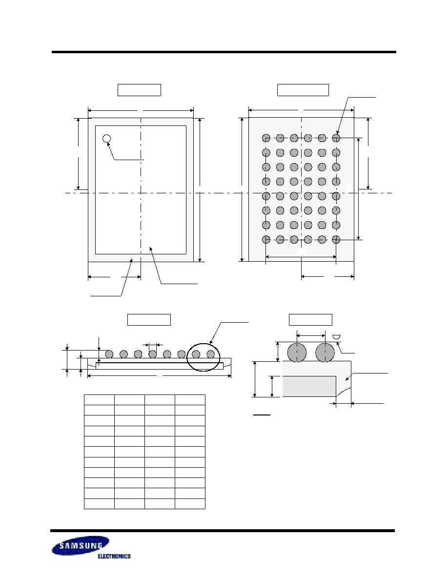
44 PIN THIN SMALL OUTLINE PACKAGE TYPE II (400F)
Units: millimeters(inches)
PACKAGE DIMENSIONS
0.002
#1
0.05
#22
#44
#23
0.35
±
0.10
0.014
±
0.004
0.80
0.0315
MIN.
0.047
1.20
MAX.
0.741
18.81
MAX.
18.41
±
0.10
0.725
±
0.004
11.76
±
0.20
0.463
±
0.008
+ 0.
10
- 0.0
5
0.50
+ 0.0
04
- 0.0
02
0.15
0.00
6
0.020
1
0
.
1
6
0
.
4
0
0
0.10
0.004
0~8
∞
0.45 ~0.75
0.018 ~ 0.030
0.25
( )
0.010
( )
0.805
0.032
( )
MAX
1.00
±
0.10
0.039
±
0.004
Revision 3.0
CMOS SRAM
K6F1016V3M, K6F1016S3M, K6F1016R3M Family
10
May 1999
Units: millimeters
PACKAGE DIMENSIONS
6
5
4
3
2
1
A
B
C
D
E
F
G
H
C
/
2
B/2
C
B
B1
C
1
Ball #A1
B
B/2
Elastomer
SRAM Die
C
Ball #A1
C
/
2
Bottom View
Top View
D
E
2
E
1
E
C
Detail A
Side View
0
.
5
5
/
T
y
p
.
0
.
3
2
/
T
y
p
.
0
.
2
5
/
T
y
p
.
A
Y
Elastomer
0.42/Typ.
Die
Detail A
Notes.
1. Bump counts: 48(8row x 6column)
2. Bump pitch: (x,y)=(0.75 x 0.75)(typ.)
3. All tolerence are +/-0.050 unless otherwise
specified.
4. Typ: Typical
5. Y is coplanarity: 0.08(Max)
Min
Typ
Max
A
-
0.75
-
B
5.90
6.00
6.10
B1
-
3.75
-
C
7.90
8.00
8010
C1
-
5.25
-
D
0.30
0.35
0.40
E
-
0.80
0.81
E1
-
0.55
-
E2
-
0.25
-
Y
-
-
0.08
48 BALL MICRO BALL GRID ARRAY- 0.75mm ball pitch