Äîêóìåíòàöèÿ è îïèñàíèÿ www.docs.chipfind.ru
K6F1616R6C Family
Revision 1.0
May 2004
1
CMOS SRAM
Document Title
1M x16 bit Super Low Power and Low Voltage Full CMOS Static RAM
Revision History
Revision No.
0.0
0.1
1.0
Remark
Preliminary
Preliminary
Final
History
Initial draft
Revised
- Changed ball name of E3 (Vss) & H6 (DNU) to NC.
- Deleted 85ns Speed bin.
Finalize
- Deleted 55ns Speed bin.
Draft Date
November 17, 2003
November 21, 2003
May 24, 2004
The attached datasheets are provided by SAMSUNG Electronics. SAMSUNG Electronics CO., LTD. reserve the right to change the specifications and
products. SAMSUNG Electronics will answer to your questions about device. If you have any questions, please contact the SAMSUNG branch offices.
K6F1616R6C Family
Revision 1.0
May 2004
2
CMOS SRAM
1M x 16 bit Super Low Power and Low Voltage Full CMOS Static RAM
GENERAL DESCRIPTION
The K6F1616R6C families are fabricated by SAMSUNG
s
advanced full CMOS process technology. The families support
industrial operating temperature ranges and have chip scale
package for user flexibility of system design. The families also
support low data retention voltage for battery back-up operation
with low data retention current.
FEATURES
·
Process Technology: Full CMOS
·
Organization: 1M x16
·
Power Supply Voltage: 1.65~1.95V
·
Low Data Retention Voltage: 1.0V(Min)
·
Three State Outputs
·
Package Type: 48-FBGA-6.00 x 7.00
Name
Function
Name
Function
CS
1
, CS
2
Chip Select Inputs
Vcc
Power
OE
Output Enable Input
Vss
Ground
WE
Write Enable Input
UB
Upper Byte(I/O
9
~
16
)
A
0
~A
19
Address Inputs
LB
Lower Byte(I/O
1
~
8
)
I/O
1
~I/O
16
Data Inputs/Outputs
NC
No Connection
PRODUCT FAMILY
1. Typical value are measured at V
CC
=1.8V, T
A
=25
°
C and not 100% tested.
Product Family
Operating Temperature
Vcc Range
Speed
Power Dissipation
PKG Type
Standby
(I
SB1
, Typ.)
Operating
(I
CC1
, Max)
K6F1616R6C-F
Industrial(-40~85
°
C)
1.65~1.95V
70ns
1
µ
A
1)
3mA
48-FBGA-6.00x7.00
SAMSUNG ELECTRONICS CO., LTD. reserves the right to change products and specifications without notice.
FUNCTIONAL BLOCK DIAGRAM
Clk gen.
Row
select
I/O
1
~I/O
8
Data
cont
Data
cont
Data
cont
I/O
9
~I/O
16
Vcc
Vss
Precharge circuit.
Memory
Cell Array
I/O Circuit
Column select
PIN DESCRIPTION
48-FBGA: Top View (Ball Down)
LB
OE
A0
A1
A2
CS2
I/O9
UB
A3
A4
CS1
I/O1
I/O10
I/O11
A5
A6
I/O2
I/O3
Vss
I/O12
A17
A7
I/O4
Vcc
Vcc
I/O13
NC
A16
I/O5
Vss
I/O15
I/O14
A14
A15
I/O6
I/O7
I/O16
A19
A12
A13
WE
I/O8
A18
A8
A9
A10
A11
NC
1
2
3
4
5
6
A
B
C
D
E
F
G
H
WE
OE
UB
CS1
LB
Control Logic
CS2
Row
Addresses
Column Addresses
K6F1616R6C Family
Revision 1.0
May 2004
3
CMOS SRAM
PRODUCT LIST
Industrial Temperature Products(-40~85
°
C)
Part Name
Function
K6F1616R6C-FF70
48-FBGA, 70ns, 1.8V
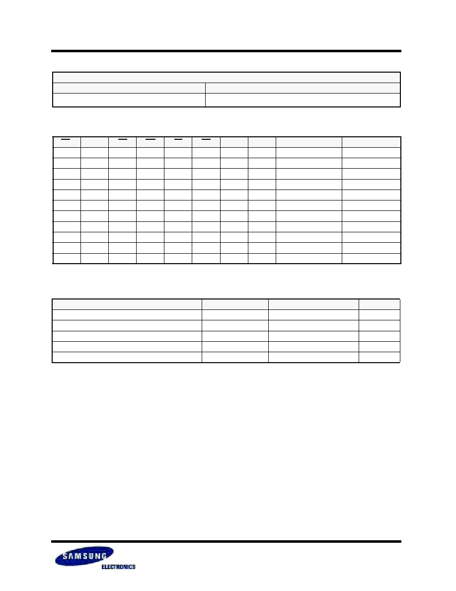
ABSOLUTE MAXIMUM RATINGS
1)
1. Stresses greater than those listed under "Absolute Maximum Ratings" may cause permanent damage to the device. Functional operation should be
restricted to recommended operating condition. Exposure to absolute maximum rating conditions for extended periods may affect reliability.
Item
Symbol
Ratings
Unit
Voltage on any pin relative to Vss
V
IN
,V
OUT
-0.2 to V
CC
+0.3V(Max. 2.6V)
V
Voltage on Vcc supply relative to Vss
V
CC
-0.2 to 2.6
V
Power Dissipation
P
D
1.0
W
Storage temperature
T
STG
-65 to 150
°
C
Operating Temperature
T
A
-40 to 85
°
C
FUNCTIONAL DESCRIPTION
1. X means don
t care. (Must be low or high state)
CS
1
CS
2
OE
WE
LB
UB
I/O
1~8
I/O
9~16
Mode
Power
H
X
1)
X
1)
X
1)
X
1)
X
1)
High-Z
High-Z
Deselected
Standby
X
1)
L
X
1)
X
1)
X
1)
X
1)
High-Z
High-Z
Deselected
Standby
X
1)
X
1)
X
1)
X
1)
H
H
High-Z
High-Z
Deselected
Standby
L
H
H
H
L
X
1)
High-Z
High-Z
Output Disabled
Active
L
H
H
H
X
1)
L
High-Z
High-Z
Output Disabled
Active
L
H
L
H
L
H
Dout
High-Z
Lower Byte Read
Active
L
H
L
H
H
L
High-Z
Dout
Upper Byte Read
Active
L
H
L
H
L
L
Dout
Dout
Word Read
Active
L
H
X
1)
L
L
H
Din
High-Z
Lower Byte Write
Active
L
H
X
1)
L
H
L
High-Z
Din
Upper Byte Write
Active
L
H
X
1)
L
L
L
Din
Din
Word Write
Active
K6F1616R6C Family
Revision 1.0
May 2004
4
CMOS SRAM
RECOMMENDED DC OPERATING CONDITIONS
1)
Note:
1. T
A
=-40 to 85
°
C, otherwise specified
2. Overshoot: V
CC
+2.0V in case of pulse width
20ns.
3. Undershoot: -2.0V in case of pulse width
20ns.
4. Overshoot and Undershoot are sampled, not 100% tested.
Item
Symbol
Min
Typ
Max
Unit
Supply voltage
Vcc
1.65
1.8
1.95
V
Ground
Vss
0
0
0
V
Input high voltage
V
IH
1.4
-
Vcc+0.2
2)
V
Input low voltage
V
IL
-0.2
3)
-
0.4
V
CAPACITANCE
1)
(f=1MHz, T
A
=25
°
C)
1. Capacitance is sampled, not 100% tested
Item
Symbol
Test Condition
Min
Max
Unit
Input capacitance
C
IN
V
IN
=0V
-
8
pF
Input/Output capacitance
C
IO
V
IO
=0V
-
10
pF
DC AND OPERATING CHARACTERISTICS
1. Typical value are measured at V
CC
=1.8V, T
A
=25
°
C and not 100% tested.
Item
Symbol
Test Conditions
Min
Typ
1)
Max
Unit
Input leakage current
I
LI
V
IN
=Vss to Vcc
-1
-
1
µ
A
Output leakage current
I
LO
CS
1
=V
IH
or CS
2
=V
IL
or OE=V
IH
or WE=V
IL
or
LB=UB=V
IH
, V
IO
=Vss to Vcc
-1
-
1
µ
A
Average operating current
I
CC1
Cycle time=1
µ
s, 100%duty, I
IO
=0mA, CS
1
0.2V,
LB
0.2V or/and UB
0.2V, CS
2
Vcc-0.2V, V
IN
0.2V or
V
IN
V
CC
-0.2V
-
-
3
mA
I
CC2
Cycle time=Min, I
IO
=0mA, 100% duty, CS
1
=V
IL
, CS
2
=V
IH
,
LB=V
IL
or/and UB=V
IL
, V
IN
=V
IL
or V
IH
-
-
22
mA
Output low voltage
V
OL
I
OL
= 0.1mA
-
-
0.2
V
Output high voltage
V
OH
I
OH
= -0.1mA
1.4
-
-
V
Standby Current(CMOS)
I
SB1
Other input =0~Vcc
1) CS
1
Vcc-0.2V, CS
2
Vcc-0.2V(CS
1
controlled) or
2) 0V
CS
2
0.2V(CS
2
controlled)
-
1
20
µ
A
K6F1616R6C Family
Revision 1.0
May 2004
5
CMOS SRAM
AC OPERATING CONDITIONS
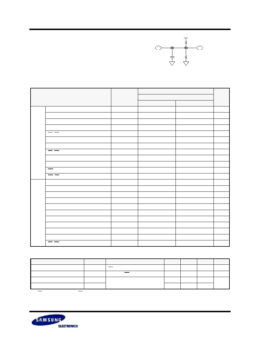
TEST CONDITIONS
(Test Load and Input/Output Reference)
Input pulse level: 0.2 to Vcc-0.2V
Input rising and falling time: 5ns
Input and output reference voltage: 0.9V
Output load(see right): C
L
=100pF+1TTL
C
L
=30pF+1TTL
DATA RETENTION CHARACTERISTICS
1.
1) CS
1
Vcc-0.2V, CS
2
Vcc-0.2V(CS
1
controlled) or
2) 0
CS
2
0.2V(CS
2
controlled)
2. Typical values are measured at T
A
=25
°
C and not 100% tested.
Item
Symbol
Test Condition
Min
Typ
2)
Max
Unit
Vcc for data retention
V
DR
CS
1
Vcc-0.2V
1)
,
V
IN
0V
1.0
-
1.95
V
Data retention current
I
DR
Vcc=1.2V, CS
1
Vcc-0.2V
1)
, V
IN
0V
-
1.0
12
µ
A
Data retention set-up time
t
SDR
See data retention waveform
0
-
-
ns
Recovery time
t
RDR
tRC
-
-
AC CHARACTERISTICS
(Vcc=1.65~1.95V, T
A
=-40 to 85
°
C)
Parameter List
Symbol
Speed Bin
Units
70ns
Min
Max
Read
Read cycle time
t
RC
70
-
ns
Address access time
t
AA
-
70
ns
Chip select to output
t
CO1
, t
CO2
-
70
ns
Output enable to valid output
t
OE
-
35
ns
LB, UB valid to data output
t
BA
-
70
ns
Chip select to low-Z output
t
LZ1
, t
LZ2
10
-
ns
Output enable to low-Z output
t
OLZ
5
-
ns
LB, UB enable to low-Z output
t
BLZ
10
-
ns
Output hold from address change
t
OH
10
-
ns
Chip disable to high-Z output
t
HZ1
, t
HZ2
0
25
ns
OE disable to high-Z output
t
OHZ
0
25
ns
UB, LB disable to high-Z output
t
BHZ
0
25
ns
Write
Write cycle time
t
WC
70
-
ns
Chip select to end of write
t
CW1
, t
CW2
60
-
ns
Address set-up time
t
AS
0
-
ns
Address valid to end of write
t
AW
60
-
ns
Write pulse width
t
WP
50
-
ns
Write recovery time
t
WR
0
-
ns
Write to output high-Z
t
WHZ
0
20
ns
Data to write time overlap
t
DW
30
-
ns
Data hold from write time
t
DH
0
-
ns
End write to output low-Z
t
OW
5
-
ns
LB, UB valid to end of write
t
BW
60
-
ns
C
L
1)
1. Including scope and jig capacitance
R
2
2)
R
1
2)
V
TM
3)
2. R
1
=3070
,
R
2
=3150
3. V
TM
=1.8V